WSQAS-9116RDLLCD KVM
Beijing Lanbe Tianhe Technoloiges & Develop CO., Ltd.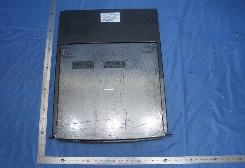
Click to zoom
Application Details
- Equipment Class
- JBP - Part 15 Class B Computing Device Peripheral
- Date of Grant
- Feb 03, 2010
- Application Purpose
- Original Equipment
- Date of Application
- Feb 03, 2010
- Equipment Note
- LCD KVM
- Country
- China
Documents & Files
Document Text
Text extracted from the exhibit documents filed with the FCC. Open a document above to read the original.
Users Manual
1 / 11 KVM User Manual KVM SWITCHES PACKING LIST Type Name Num/UnitNote AS-3100L Series Products KVM Control Platform 1 15 inches LCD screen, keyboard and mouse control platform integrated KVM switch with multiple ports (4/8/16ports). AS-7100L Series Products KVM Control Platform 1 17 inches LCD screen, keyboard and mouse control platform integrated KVM switch with multiple ports (4/8/16ports). AS-9100L Series Products KVM Control Platform 1 19 inches LCD screen, keyboard and mouse control platform integrated KVM switch with multiple ports (4/8/16ports). Cable KVM Connecting Cable 1/4/8/16 PS/2 Connecting and USB Connecting AC Power Power Cable 1 AC power connecting cable KVM Control User Manual User Manual 1/2 LCD Manual and KVM Manual Please check the lists carefully and contact with your dealer if you have some problems. Please read the manual carefully before installation. Assembling & Disassembling The device can be assembled and disassembled as following. 2 / 11 3 / 11 OVERVIEW KVM control platform is one witch integrate a multiple ports KVM switch into 1U height. It controls multiple computers with one platform (keyboard, mouse and monitor). A KVM switch can control 4/8/16 PC by direct connection and it can control 256 PC at most by 3 level cascade connection. It is easy and quick to install. Just connect the wire to the correct port without software configuration. So there is no difficulty in installation and incompatibility. KVM switch provides two methods to control the computers connected to it: 1. By keyboard combine key. 2. By OSD operation. In addition, it provides powerful automatic scanning function to scan and monitor all computers 4 / 11 connected to it. Using KVM control platform is a best choice to save time and money. By using one KVM platform to manage all the computers connected to it, user can save money for keyboard, mouse and monitor for each computer and their space. PRODUCT TYPE Type OSD Function Note AS-3100L No 15 inches LCD screen, keyboard and mouse. And Body parts can be easily demolished AS-3104\ 08\16RDL Ye s 15 inches LCD screen, keyboard, mouse and 4\8\16 ports PS/2 KVM. And Body parts can be easily demolished AS-3104\ 08\16UDL Ye s 15 inches LCD screen, keyboard, mouse and 4\8\16 ports USB KVM. And Body parts can be easily demolished AS-7100L No 17 inches LCD screen, keyboard and mouse. And Body parts can be easily demolished AS-7104\ 08\16RDL Ye s 17 inches LCD screen, keyboard, mouse and 4\8\16 ports PS/2 KVM. And Body parts can be easily demolished AS-7104\ 08\16UDL Ye s 17 inches LCD screen, keyboard, mouse and 4\8\16 ports USB KVM. And Body parts can be easily demolished AS-9100L No 19 inches LCD screen, keyboard and mouse. And Body parts can be easily demolished AS-9104\ 08\16RDL Ye s 19 inches LCD screen, keyboard, mouse and 4\8\16 ports PS/2 KVM .And Body parts can be easily demolished AS-9104\ 8\16UDL Ye s 19 inches LCD screen, keyboard, mouse and 4\8\16 ports USB KVM .And Body parts can be easily demolished FEATURES Control Platform Control platform with LCD, keyboard, mouse and multiple ports KVM switch. 1U height, suitable for 19’’ standard cabinet installation and metal structure. 15/17/19’’ LCD screen with high brightness, high clear and high resolution. Control platform can be totally pulled out from the cabinet and the LCD screen can be turned on to 120 degrees. Ultra thin keyboard with keypad. Mouse touch board with two function button. Front panel with lock to prevent damage by accident. Built-in power. Automatic power on/off. When pulling control platform out from cabinet, the power turns off automatically. When pushing it into the cabinet, the power turns on automatically. An easy to use OSD menu. 5 / 11 Switch One control platform can control 4/ 8/16 computers by direct connection. One control platform can control 256 computers by 3 level cascade connection. Be compatible with PS/2, USB standard interface. Support VGA, SVGA, XGA video input. Accord with DDC, DDC2, DDC2B standard and VESA standard. Support maximum resolution of 1920 * 1440 Support multiple operating systems: WIN95/98/98SE/ME/200/XP、WIN NT、UNIX、LINUX. FRONT VIEW 1. Front panel 2. Handle 3. LCD screen 4. Keyboard 5. Mouse touch board 6. Rear hang ear channel 7. Guide 8. Front hang ear 9. LCD OSD control key 1 2 3 4 5 6 7 8 9 REAR VIEW AS-3104UDL/AS-7104UDL/AS-9104UDL AS-3108UDL/AS-7108UDL/AS-9108UDL 6 / 11 AS-3116UDL/AS-7116UDL/AS-9116UDL ① ② ① AC 100~230V power socket ② PC connecting port AS-3104UDL/AS-7104UDL/AS-9104UDL AS-3108UDL/AS-7108UDL/AS-9108UDL AS-3116UDL/AS-7116UDL/AS-9116UDL ① DC 9V 1000mA power socket ② PC connecting port KVM CONTROL PLATFORM CONNECTING WIRE Cable Type Applicable Type KVM Port PC or Server Port USB Connecting Cable AS-3104/08/16UDL Series Products VGA port (Keyboard, mouse and monitor) VGA、Keyboard、Mouse (Standard USB Interface) PS/2 Connecting Cable AS-3104/08/16RDL Series Products VGA Port (Keyboard mouse And monitor) VGA、Keyboard、Mouse (Standard PS/2 Interface) 7 / 11 USB Connecting 1.8m Cable PS/2 Connecting 1.8m Cable USB and PS/2 Connecting 1.8m Cable KVM CONTROL PLATFORM POWER WIRE Wire Type Note Voltage Range Machine Type AC Power Wire 3 Plugs of National Standard 100~230V All 8 / 11 AC Power Wire DIMENSION CONNECTION OF KVM SIGNAL WIRE 1. PS/2 connecting wire Connect the end with 3 sockets to the KVM control platform, and the other to the computer. 2. USB connecting wire 9 / 11 Connect the end with HD15 to the USB KVM control platform, and the other to the computer. OPERATIO Before Use z Make sure all the devices safely grounded. z Make sure the KVM wire and power wire connected correctly. During Use z Pull the KVM control platform out from cabinet totally, the guide locks automatically and the power turns on. z Release front lock. As shown below: 10 / 11 z Then open the front panel and the LCD can be turn on to 120 degrees. As shown below: UNLOCK AUTO LOCK z Press LCD power key (red), the LCD is on. After U…
Text truncated - open the document above for the full version.
Cover Letter(s)
FCC ID: WSQAS-9116RDL POWER OF ATTORNEY Jan.20, 2010 Federal Communications Commission Authorization and Evaluation Division 7435 Oakland Mills Road Columbia, MD 21046 To Whom It May Concern: We, the undersigned, hereby authorize Waltek Services (ShenZhen) Co., Ltd. (Philo Zhong) on our behalf, to apply to the Federal Communications Commission on our equipment. Any and all acts carried out by Waltek Services (ShenZhen) Co., Ltd. (Philo Zhong) on our behalf shall have the same effect as acts of our own. This authorization expires on Jan.21,2011 This is to advise that we are in full compliance with the Anti-Drug Abuse Act. We, Beijing Lanbe Tianhe Technologies&Develop CO., Ltd.are not subject to a denial of federal benefits pursuant to Section 5301 of the Anti-Drug Act of 1988, 21 USC853a, and no party to the application is subject to a denial of federal benefits pursuant to that section. Sincerely, Beijing Lanbe Tianhe Technologies&Develop CO., Ltd. .................................... Manager
External Photos
EUT - Top View(AS-9116RDL) EUT – Bottom View(AS-9116RDL) EUT - Front View(AS-9116RDL) EUT - Back View(AS-9116RDL)
ID Label/Location Info
FCC ID Label This device complies with Part 15 of the FCC Rules. Operation is subject to the following two conditions:(1)this device may not cause harmful interference, and (2) this device must accept any interference received, including interference that may cause undesired operation. The Label must not be a stick-on paper. The Label on these products must be permanently affixed to the product and readily visible at the time of purchase and must last the expected lifetime of the equipment not be readily detachable. Proposed Label Location on EUT EUT Top View/ proposed FCC Label Location FCC ID: WSQAS-9116RDL This device complies with Part 15 of the FCC Rules. Operation is subject to the following two conditions:(1)this device may not cause harmful interference,and (2) this device must accept any interference received, including interference that may cause undesired operation
ID Label/Location Info
FCC ID Label Sample for Model AS-3100L, AS-3104UDL, AS-3108UDL, AS-3116UDL, AS-3104RDL, AS-3108RDL, AS-3116RDL, AS-7100L, AS-7104UDL, AS-7108UDL, AS-7116UDL, AS-7104RDL, AS-7108RDL, AS-7116RDL, AS-9100L, AS-9104UDL AS-9108UDL,AS-9116UDL, AS-9104RDL, AS-9108RDL, AS-9116RDL FCC ID : WSQAS-9116RDL This device complies with Part 15 of the FCC Rules. Operation is subject to the following two conditions:(1)this device may not cause harmful interference, and (2) this device must accept any interference received, including interference that may cause undesired operation.
Internal Photos
EUT - Open View(AS-9116RDL) 1 EUT - Open View(AS-9116RDL) 2 EUT- Open View(AS-9116RDL)3 EUT - Open View(AS-9116RDL)4 PCB 1 –Top View(AS-9116RDL) PCB 1 - Bottom View(AS-9116RDL) PCB 2 -Top View(AS-9116RDL) PCB 2 - Bottom View(AS-9116RDL) PCB 3 -Top View(AS-9116RDL) PCB 3 - Bottom View(AS-9116RDL) PCB 4 -Top View(AS-9116RDL) PCB 4 - Bottom View(AS-9116RDL) PCB 5-Top View(AS-9116RDL) PCB 5 - Bottom View(AS-9116RDL) PCB 6 -Front View(AS-9116RDL) PCB 6 -Back View(AS-9116RDL) PCB 7 -Front View(AS-9116RDL) PCB 7 -Back View(AS-9116RDL)
Operational Description
Circuit description LCD KVM SWITCH KVM switch can be a good solution to a single person to multiple servers or an entire room of the PC server routine management and maintenance. Equipment will be a very good LCD monitor, ultra-thin keyboard and touch mouse combination intact, eliminating the complexity of the interface cable is more space-saving machine. It is more than one server or PC mouse, keyboard, VGA signal input through the input port, through the device comes with mouse, keyboard and display control port to operate. KVM keyboard and mouse signals will VGA signal through the selector, according to the needs of controllers. To send commands to the microcontroller and microcontroller upon receipt of order to give the choice of chip for each port to send commands to selector switch to the user needs a single PC or server to operate! 1, input VGA signal through the resistor after the matched-impedance input to the selector chip, and then select the device directly from the MCU control, the operator sends commands to the microcontroller and microcomputer control VGA signal selector select a group of users need to VGA signal, the user selector need to VGA signal to the integrated op-amp chip signal amplification transmission to the control side of the display, in order to achieve choice! 2, the input signal directly to the mouse and keyboard signals into the microcontroller, microcontroller according to the user's requirements need to control the choice of server or PC, microcontroller also sends instructions to ensure the mouse, keyboard, and VGA signal synchronization work! MCU external oscillator frequency of the main directives 22.1184MHZ, auxiliary instruction oscillation frequency of the external MCU 24MHZ, USB signal processing microcontroller external oscillation frequency 48MHZ, PS / 2 signal processing microcontroller external oscillation frequency 20MHZ. LCD Monitor VGA signal drive circuit external oscillation frequency 14.318 MHZ! The above circuit description KVM's work!
Schematics
123456789101112 A B C D 121110987654321 D C B A RED1RED2RED7RED4 GRE1GRE2GRE7GRE4 BLU1BLU2BLU7BLU4 HSY1HSY2HSY7HSY4 VSY1VSY2VSY7VSY4 UP1VCCUP2VCCUP7VCCUP4VCC UP1DATA-UP2DATA-UP7DATA-UP4DATA- UP1DATA+UP2DATA+UP7DATA+UP4DATA+ RED8RED6RED3RED5 GRE8GRE6GRE3GRE5 BLU8BLU6BLU3BLU5 HSY8HSY6HSY3HSY5 VSY8VSY6VSY3VSY5 UP8VCCUP6VCCUP3VCCUP5VCC UP8DATA-UP6DATA-UP3DATA-UP5DATA- UP8DATA+UP6DATA+UP3DATA+UP5DATA+ HSYO VSYO GND GND 1 2 3 4 5 6 7 8 9 10 11 12 13 14 15 16 17 J1 DB15 1 2 3 4 5 6 7 8 9 10 11 12 13 14 15 16 17 J2 DB15 1 2 3 4 5 6 7 8 9 10 11 12 13 14 15 16 17 J3 DB15 1 2 3 4 5 6 7 8 9 10 11 12 13 14 15 16 17 J4 DB15 1 2 3 4 5 6 7 8 9 10 11 12 13 14 15 16 17 J5 DB15 1 2 3 4 5 6 7 8 9 10 11 12 13 14 15 16 17 J6 DB15 1 2 3 4 5 6 7 8 9 10 11 12 13 14 15 16 17 J7 DB15 1 2 3 4 5 6 7 8 9 10 11 12 13 14 15 16 17 J8 DB15 1 2 3 4 5 6 7 8 9 10 11 12 13 14 15 16 17 J9 DB15 KEY_SDA1KEY_SDA2KEY_SDA3KEY_SDA4KEY_SDA5KEY_SDA6KEY_SDA7KEY_SDA8 KEY_SCLK1KEY_SCLK2KEY_SCLK3KEY_SCLK4KEY_SCLK5KEY_SCLK6KEY_SCLK7KEY_SCLK8 GND GND GND GND GND GND GND GND GND GND GND GND GNDGND GNDGND GND GND GND GND GND GND GND GND GND GND GND GND GND GND GND GND GND GND GND GND GND GND GND GND GND GND GND GND GND X0 13 X1 14 X2 15 X3 12 X4 1 X5 5 X6 2 X7 4 INH 6 A 11 B 10 C 9 VEE 7 X 3 V C C 1 6 G N D 8 U9 74HC4051 RED1 RED2 RED7 RED4 GRE1 GRE2 GRE7 GRE4 BLU1 BLU2 BLU7 BLU4 RED8 RED6 RED3 RED5 GRE8 GRE6 GRE3 GRE5 BLU8 BLU6 BLU3 BLU5 X0 13 X1 14 X2 15 X3 12 X4 1 X5 5 X6 2 X7 4 INH 6 A 11 B 10 C 9 VEE 7 X 3 V C C 1 6 G N D 8 U11 74HC4051 X0 13 X1 14 X2 15 X3 12 X4 1 X5 5 X6 2 X7 4 INH 6 A 11 B 10 C 9 VEE 7 X 3 V C C 1 6 G N D 8 U10 74HC4051 RED0GRE0BLU0 AVCCAVCC S0-1 S1-1 S2-1 /CE3 S0-1 S1-1 S2-1 /CE3 S0-1 S1-1 S2-1 /CE3 5 6 7 U28B SGM8094 R57 751 R56 751 3 2 1 4 1 1 U28A SGM8094 R44 751 R43 751 10 9 8 U28C SGM8094 R53 751 R52 751 RED0 GRE0 BLU0 S_RED S_BLU S_GRE R55 750 R45 750 R42 750 REDO GREO BLUO A/B 1 1A 2 1B 3 1Y 4 2A 5 2B 6 2Y 7 GND 8 3Y 9 3B 10 3A 11 4Y 12 4B 13 4A 14 G 15 VCC 16 U44 PI5V330Q AVCC S_RED S_BLU S_GRE OSD_RED OSD_GRE OSD_BLU OSD_FBKG R47 103 VCC VSSA 1 VCO 2 RP 3 VDDA 4 HFLB 5 SSB 6 SDA 7 SCK 8 VDD 9 VFLB 10 HTONE/ 11 FBKG 12 BOUT 13 GOUT 14 ROUT 15 VSS 16 U41 MTV018 C84 222 C82 473 C81 104 C83 104 OSD_RED OSD_GRE OSD_BLU OSD_FBKG VSY0 HSY0 SDA_C SCK_C AVCC VCC C85 47pF R65 511 R66 511 R67 511 R61 202 R62 202 R63 105 R64 302 HSY_C VSY_C HSY_C0 VSY_C0 A/B 1 1A 2 1B 3 1Y 4 2A 5 2B 6 2Y 7 GND 8 3Y 9 3B 10 3A 11 4Y 12 4B 13 4A 14 G 15 VCC 16 U21 PI5V330Q VCC A HSY0 VSY0 HSY1 HSY2 HSY7 HSY4 VSY1 VSY2 VSY7 VSY4 HSY8 HSY6 HSY3 HSY5 VSY8 VSY6 VSY3 VSY5 HSY_CVSY_C S1_SMOSI_FPGA S1_SCLK_FPGA S2_SMOSI_FPGA S2_SCLK_FPGA S3_SMOSI_FPGA S3_SCLK_FPGA S4_SMOSI_FPGA S4_SCLK_FPGA S8_SMOSI_FPGA S8_SCLK_FPGA S7_SMOSI_FPGA S7_SCLK_FPGA S5_SMOSI_FPGA S5_SCLK_FPGA S6_SMOSI_FPGA S6_SCLK_FPGA P0.7 1 P0.6 2 P0.5 3 P0.4 4 P0.3 5 P0.2 6 P0.1 7 P0.0 8 VSS 9 P1.0/D+ 10 P1.1/D- 11 VCC 12 P1.2 13 SSEL 14 SCLK 15 SMOSI 16 SMISO 17 P1.7 18 U29 CY63813 UP1VCC P0.7 1 P0.6 2 P0.5 3 P0.4 4 P0.3 5 P0.2 6 P0.1 7 P0.0 8 VSS 9 P1.0/D+ 10 P1.1/D- 11 VCC 12 P1.2 13 SSEL 14 SCLK 15 SMOSI 16 SMISO 17 P1.7 18 U32 CY63813 UP2VCC P0.7 1 P0.6 2 P0.5 3 P0.4 4 P0.3 5 P0.2 6 P0.1 7 P0.0 8 VSS 9 P1.0/D+ 10 P1.1/D- 11 VCC 12 P1.2 13 SSEL 14 SCLK 15 SMOSI 16 SMISO 17 P1.7 18 U30 CY63813 P0.7 1 P0.6 2 P0.5 3 P0.4 4 P0.3 5 P0.2 6 P0.1 7 P0.0 8 VSS 9 P1.0/D+ 10 P1.1/D- 11 VCC 12 P1.2 13 SSEL 14 SCLK 15 SMOSI 16 SMISO 17 P1.7 18 U33 CY63813 UP4VCC UP1DATA+ UP2DATA+ UP3DATA+ UP4DATA+ UP1DATA- UP2DATA- UP3DATA- UP4DATA- D3 SS14 D4 SS14 D7 SS14 D6 SS14 P0.7 1 P0.6 2 P0.5 3 P0.4 4 P0.3 5 P0.2 6 P0.1 7 P0.0 8 VSS 9 P1.0/D+ 10 P1.1/D- 11 VCC 12 P1.2 13 SSEL 14 SCLK 15 SMOSI 16 SMISO 17 P1.7 18 U35 CY63813 UP7VCC P0.7 1 P0.6 2 P0.5 3 P0.4 4 P0.3 5 P0.2 6 P0.1 7 P0.0 8 VSS 9 P1.0/D+ 10 P1.1/D- 11 VCC 12 P1.2 13 SSEL 14 SCLK 15 SMOSI 16 SMISO 17 P1.7 18 U36 CY63813 UP8VCC P0.7 1 P0.6 2 P0.5 3 P0.4 4 P0.3 5 P0.2 6 P0.1 7 P0.0 8 VSS 9 P1.0/D+ 10 P1.1/D- 11 VCC 12 P1.2 13 SSEL 14 SCLK 15 SMOSI 16 SMISO 17 P1.7 18 U34 CY63813 P0.7 1 P0.6 2 P0.5 3 P0.4 4 P0.3 5 P0.2 6 P0.1 7 P0.0 8 VSS 9 P1.0/D+ 10 P1.1/D- 11 VCC 12 P1.2 13 SSEL 14 SCLK 15 SMOSI 16 SMISO 17 P1.7 18 U31 CY63813 UP5VCC UP7DATA+ UP8DATA+ UP6DATA+ UP5DATA+ UP7DATA- UP8DATA- UP6DATA- UP5DATA- D17 SS14 D8 SS14 D5 SS14 D21 SS14 UP6VCC UP3VCC KEY_LED1_1 KEY_LED2_1 KEY_LED3_1 KEY_LED4_1 KEY_LED1_4 KEY_LED2_4 KEY_LED3_4 KEY_LED4_4 KEY_LED1_2 KEY_LED2_2 KEY_LED3_2 KEY_LED4_2 KEY_LED1_3 KEY_LED2_3 KEY_LED3_3 KEY_LED4_3 KEY_LED1_5 KEY_LED2_5 KEY_LED3_5 KEY_LED4_5 KEY_LED1_7 KEY_LED2_7 KEY_LED3_7 KEY_LED4_7 KEY_LED1_6 KEY_LED2_6 KEY_LED3_6 KEY_LED4_6 KEY_LED1_8 KEY_LED2_8 KEY_LED3_8 KEY_LED4_8 KEY_SCLK3 KEY_SDA3 KEY_SCLK5 KEY_SDA5 KEY_SCLK1 KEY_SDA1 KEY_SCLK2 KEY_SDA2 KEY_SCLK4 KEY_SDA4 KEY_SCLK6 KEY_SDA6 KEY_SCLK7 KEY_SDA7 KEY_SCLK8 KEY_SDA8 1 2 3 4 5 6 7 8 GND GND GND GND GND GND GND GND C75 104 C73 104 C71 104 C69 104 C76 104 C74 104 C72 104 C70 104 UP1VCC UP2VCC UP7VCC UP4VCC UP8VCC UP6VCC UP3VCC UP5VCC 1 2 3 4 5 6 7 8 R29 102 R30 102 R31 102 R32 102 R33 102 R34 102 R35 102 R36 102 TEST1 TEST2 TEST3 TEST4 TEST5 TEST6 TEST7 TEST8 R132 103 R133 103 R134 103 R135 103 R136 103 R137 103 R138 103 R139 103 R124 103 R125 103 R126 103 R127 103 R128 103 R129 103 R130 103 R131 103 C5 47P C6 47P C7 47P C8 47P C10 47P C32 47P C33 47P C39 47P C45 47P C47 47P C11 47P C12 47P C18 47P C51 47P C52 47P C53 47P S1_SCLK_FPGA S2_SCLK_FPGA S3_SCLK_FPGA S4_SCLK_FPGA S5_SCLK_FPGA S6_SCLK_FPGA S7_SCLK_FPGA S8_SCLK_FPGA S1_SMOSI_FPGA S2_SMOSI_FPGA S3_SMOSI_FPGA S4_SMOSI_FPGA S5_SMOSI_FPGA S6_SMOSI_FPGA S7_SMOSI_FPGA S8_SMOSI_FPGA X0 13 X1 14 X2 15 X3 12 X4 1 X5 5 X6 2 X7 4 INH 6 A 11 B 10 C 9 VEE 7 X 3 U5 74HC4051 X0 13 X1 14 X2 15 X3 12 X4 1 X5 5 X6 2 X7 4 INH 6 A 11 B 10 C 9 VEE 7 X 3 U6 74HC4051 KEY_LED1KEY_LED2KEY_LED1_1KEY_LED2_1 KEY_LED3_1KEY_LED4_1 KEY_LED1_4KEY_LED2_4 KEY_LED3_4KEY_LED4_4 KEY_LED1_2KEY_LED2_2 KEY_LED3_2KEY_LED4_2 KEY_LED1_3KEY_LED2_3 KEY_LED3_3KEY_LED4_3 KEY_LED1_5KEY_LED2_5 KEY_LED3_5KEY_LED4_5 KEY_LED1_7KEY_LED2_7 KEY_LED3_7KEY_LED…
Text truncated - open the document above for the full version.
Test Report
Beijing Lanbe Tianhe Technologies&Develop CO., Ltd. FCC ID: WSQAS-9116RDL FCC TEST REPORT Page: 1 of 34 FCC ID : WSQAS-9116RDL Applicant : Beijing Lanbe Tianhe Technologies&Develop CO., Ltd. Address : Room 508,Guoxin Building, SHOUT:Nan Rd. NO.20,Haidian District,Beijing,China Equipment Under Test (EUT) : Product description : LCD KVM Model No. : AS-3100L, AS-3104UDL, AS-3108UDL, AS-3116UDL, AS-3104RDL, AS-3108RDL, AS-3116RDL, AS-7100L, AS-7104UDL, AS-7108UDL, AS-7116UDL, AS-7104RDL, AS-7108RDL, AS-7116RDL, AS-9100L, AS-9104UDL AS-9108UDL,AS-9116UDL, AS-9104RDL, AS-9108RDL, AS-9116RDL Standards : FCC Part 15 Subpart B Date of Test : Jan. 08, 2010 Test Engineer :Maikou.zhang Reviewed By : Test Result : PASS * PERPARED BY: Waltek Services (Shenzhen) Co., Ltd. 1/F, Fukangtai Building,West Baima Rd.,Songgang Street, Baoan District, Shenzhen 518105,China Tel :+86-755-27553488 Fax:+86-755-27553868 . Beijing Lanbe Tianhe Technologies&Develop CO., Ltd. FCC ID: WSQAS-9116RDL Page:2 of 34 1 Test Summary Test Test RequirementTest Method Class / Severity Result Radiated Emission (30MHz to 2GHz) FCC PART 15, SUBPART B: 2007 ANSI C63.4: 2009 Class B PASS Conducted Emission (150KHz to 30MHz) FCC PART 15, SUBPART B: 2007 ANSI C63.4: 2009 Class B PASS Beijing Lanbe Tianhe Technologies&Develop CO., Ltd. FCC ID: WSQAS-9116RDL Page:3 of 34 Contents 1 COVER PAGE ......................................................................................................................................................... 1 1 TEST SUMMARY........................................................................................................................................................ 2 CONTENTS ...................................................................................................................................................................... 3 2 GENERAL INFORMATION ................................................................................................................................ 5 2.1 CLIENT INFORMATION........................................................................................................................................... 5 2.2 GENERAL DESCRIPTION OF E.U.T. ........................................................................................................................ 5 2.3 DETAILS OF E.U.T................................................................................................................................................. 6 2.4 DESCRIPTION OF SUPPORT UNITS.......................................................................................................................... 6 2.5 STANDARDS APPLICABLE FOR TESTING................................................................................................................ 6 2.6 TEST FACILITY...................................................................................................................................................... 7 2.7 TEST LOCATION.................................................................................................................................................... 7 3 EQUIPMENT USED DURING TEST .................................................................................................................. 8 4 EMISSIONS TEST RESULTS ............................................................................................................................ 11 4.1 CONDUCTED EMISSION DATA............................................................................................................................. 11 4.1.1 E.U.T. Operation ...................................................................................................................................... 11 4.1.2 EUT Setup ................................................................................................................................................. 12 4.1.3 Conducted Emission Test Data................................................................................................................. 13 4.1.4 Photographs – Conducted Emission Test Setup ....................................................................................... 14 4.2 RADIATION EMISSION DATA...............................................................................................................................15 4.2.1 Measurement Uncertainty......................................................................................................................... 15 4.2.2 EUT Setup ................................................................................................................................................. 16 4.2.3 Test Procedure.......................................................................................................................................... 16 4.2.4 Spectrum Analyzer Setup .......................................................................................................................... 17 4.2.5 ThCorrected Amplitude & Margin Calculation........................................................................................ 18 4.2.6 Summary of Test Results ........................................................................................................................... 18 4.2.7 Photographs – Radiation Emission Test Setup......................................................................................... 21 5 PHOTOGRAPHS - CONSTRUCTIONAL DETAILS...................................................................................... 22 5.1 EUT - TOP VIEW(AS-9116RDL) ........................................................................................................................ 22 5.2 EUT – BOTTOM VIEW(AS-9116RDL) ................................................................................................................ 22 5.3 EUT - FRONT VIEW(AS-9116RDL)..........................................................................…
Text truncated - open the document above for the full version.
Test Setup Photos
Photographs of Testing Radiation Emission Test View Below 1G Above 1G Conducted Emission Test Setup View
Contact Information
Applicant
Li hua cui(Manager)
Test Firm
Waltek Services(Shenzhen) Co., Ltd.Philo zhong
Technical Specifications
| # | Rule Parts | Frequency Range | Power Output |
|---|---|---|---|
| 1 | 15B | - | - |
Other Applications from Beijing Lanbe Tianhe Technoloiges & Develop CO., Ltd.
WSQKSSERIES
Mar 27, 2011KVM SWITCH
Equipment Class
JBP - Part 15 Class B Computing Device Peripheral
WSQMVSSERIES
Apr 11, 2010SWITCH VIDEO SPLITTER
Equipment Class
JBP - Part 15 Class B Computing Device Peripheral
WSQAS-3116DU
Feb 01, 2010KVM SWITCH
Equipment Class
JBP - Part 15 Class B Computing Device Peripheral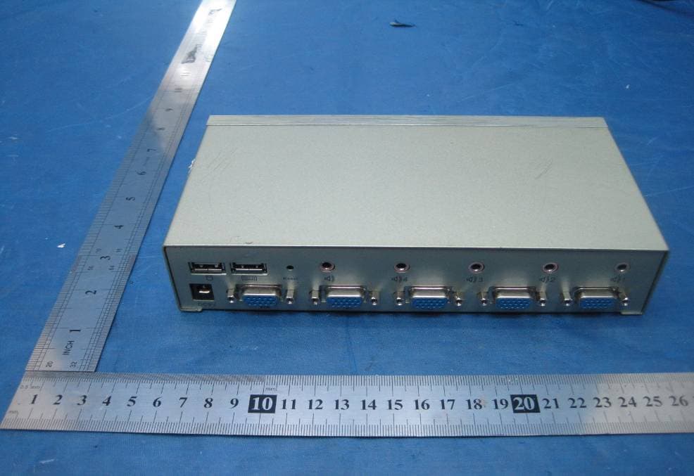
WSQAS-41P
Jan 28, 2010KVM SWITCH
Equipment Class
JBP - Part 15 Class B Computing Device Peripheral