WSQKSSERIESKVM SWITCH
Beijing Lanbe Tianhe Technoloiges & Develop CO., Ltd.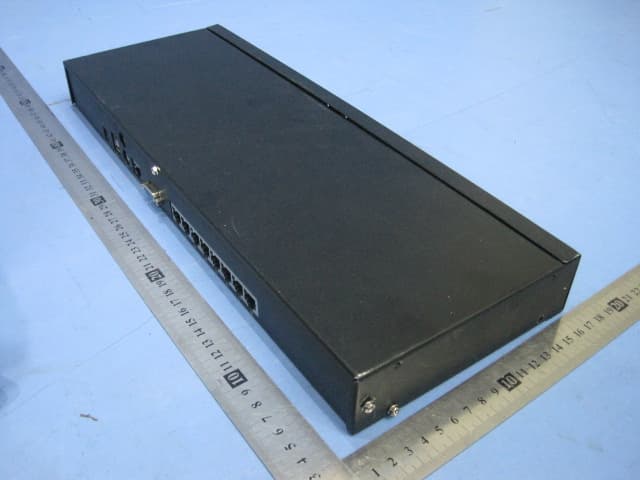
Click to zoom
Application Details
- Equipment Class
- JBP - Part 15 Class B Computing Device Peripheral
- Date of Grant
- Mar 27, 2011
- Application Purpose
- Original Equipment
- Date of Application
- Mar 27, 2011
- Equipment Note
- KVM SWITCH
- Country
- China
Documents & Files
Document Text
Text extracted from the exhibit documents filed with the FCC. Open a document above to read the original.
Users Manual
User Manual FCC NOTE This equipment has been tested and found to comply with the limits for a class B digital device, pursuant to part 15 of the FCC rules. These limits are designed to provide reasonable protection against harmful interference in a residential installation. This equipment generates, uses and can radiate radio frequency energy and, if not installed and used in accordance with the instruction manual, may cause harmful interference to radio communications. However, there is no guarantee that interference will not occur in a particular installation. If this equipment does cause harmful interference to radio or television reception, which can be determined by turning the equipment off and on, the user is encouraged to try to correct the interference by one or more of the measures listed below. Reorient or relocate the receiving antenna. Increase the separation between the equipment and receiver. Connect the equipment into an outlet on a circuit different from that to which the receiver is connected. Consult the dealer or an experienced radio/television technician for help. This device complies with Part 15 of the FCC Rules. Operation is subject to the following two conditions:(1)this device may not cause harmful interference, and (2) this device must accept any interference received, including interference that may cause undesired operation. The manufacturer is not responsible for any radio or TV interference caused by unauthorized modifications to this equipment. Such modifications could void the user's authority to operate the equipment. PACKING LIST The complete 8 ports/16 ports PS/2 / USB switch package consists of: 8 ports/16 ports PS/2 / USB switch Power Adapter User Manual Please check to make sure that all the components are present and that nothing was damaged in shipping. If you encounter a problem, contact your dealer. Read this manual thoroughly and follow the installation and operation procedure carefully to prevent any damage to the unit, and/or any of the devices that connect to it. ©Copyright 2010 LANBE® Co.,Ltd OVERVIEW .................................................................................................................................................................................... 3 FEATURES ..................................................................................................................................................................................... 3 HARDWARE REQUIREMENTS................................................................................................................................................... 3 CONSOLE .............................................................................................................................................................................. 3 COMPUTER ........................................................................................................................................................................... 3 INTRODUCTION........................................................................................................................................................................... 4 KS-3108 FRONT VIEW ......................................................................................................................................................... 4 KS-3116 FRONT VIEW ......................................................................................................................................................... 4 KS-3108 REAR VIEW............................................................................................................................................................ 5 KS-3116 REAR VIEW............................................................................................................................................................ 5 INSTALLATION............................................................................................................................................................................. 6 BEFORE YOU BEIGIN.......................................................................................................................................................... 6 SINGLE STAGE INSTALLATION ........................................................................................................................................ 6 OPERATION................................................................................................................................................................................... 7 HOT PLUGGING ................................................................................................................................................................... 7 POWERING OFF AND RESTARTING ................................................................................................................................. 7 PORT SELECTION ................................................................................................................................................................ 7 OSD OPERATION.......................................................................................................................................................................... 8 OSD OVERVIEW ................................................................................................................................................................... 8 OSD NAVIGATION................................................................................................................................................................ 8 OSD MAIN SCREEN HEADINGS........................................................................................................................................ 9 OSD FUNCTIONS.................................................................................................................................................…
Text truncated - open the document above for the full version.
Block Diagram
KS Series Block Diagram KT-150/KT- 250 Encoder KT-150/KT- 250 Encoder KT-150/KT- 250 Encoder KS-3104 KS-3108 KS-3116 switch/ Decoder /output Local control Working Frequency 11.952MHZ P C 1 P C 2 P C 16 P C 1 5 KT-150/KT- 250Encoder
Cover Letter(s)
FCC ID: WSQKSSERIES POWER OF ATTORNEY MAR.21, 2011 Federal Communications Commission Authorization and Evaluation Division 7435 Oakland Mills Road Columbia, MD 21046 To Whom It May Concern: We, the undersigned, hereby authorize Waltek Services (ShenZhen) Co., Ltd. (Philo Zhong) on our behalf, to apply to the Federal Communications Commission on our equipment. Any and all acts carried out by Waltek Services (ShenZhen) Co., Ltd. (Philo Zhong) on our behalf shall have the same effect as acts of our own. This authorization expires on Mar.20,2012 This is to advise that we are in full compliance with the Anti-Drug Abuse Act. We, Beijing Lanbe Tianhe Technologies&Develop CO., Ltd.are not subject to a denial of federal benefits pursuant to Section 5301 of the Anti-Drug Act of 1988, 21 USC853a, and no party to the application is subject to a denial of federal benefits pursuant to that section. Sincerely, Beijing Lanbe Tianhe Technologies&Develop CO., Ltd. .................................... Manager
External Photos
2.1 EUT - Front View 2.2 EUT - Back View
ID Label/Location Info
2 FCC ID Label This device complies with Part 15 of the FCC Rules. Operation is subject to the following two conditions:(1)this device may not cause harmful interference, and (2) this device must accept any interference received, including interference that may cause undesired operation. The Label must not be a stick-on paper. The Label on these products must be permanently affixed to the product and readily visible at the time of purchase and must last the expected lifetime of the equipment not be readily detachable. Proposed Label Location on EUT EUT Top View/ proposed FCC Label Location FCC ID: WSQKSSERIES This device complies with Part 15 of the FCC Rules. Operation is subject to the following two conditions:(1)this device may not cause harmful interference,and (2) this device must accept any interference received, including interference that may cause undesired operation.
ID Label/Location Info
FCC ID Label Sample for Model: KS-3116 (KT-150); KS-3116 (KT-250); KS-3108 (KT-150); KS-3108 (KT-250); KS-3104 (KT-150); KS-3104£ ̈KT-250) FCC ID: WSQKSSERIES This device complies with Part 15 of the FCC Rules. Operation is subject to the following two conditions: (1)this device may not cause harmful interference, and (2) this device must accept any interference received, including interference that may cause undesired operation.
Internal Photos
2.1 EUT-PCB -Front View 2.2 EUT-PCB - Back View
Operational Description
Circuit Description PC or server through the KT-150 (USB interface) or KT-250 (PS / 2 interface) encoder (the computer's mouse, keyboard signals through the IC (IC operating frequency 11.952MHZ) into RS-485 differential signal transmission. VGA display signal into a differential signal through the IC, the two differential signal transmission to the encoder of the RJ45 interface. After a CAT5 type cable transmission decoder KS-3104 3108 3116 to RJ45 differential signal interface, After the remote and local control personnel microcontroller input control instruction command and then send commands to the microcontroller input KS series switch IC, Have a choice to set the user's PC or server or select signal 1: the mouse, keyboard, switch to the KS series of decoders for RS-485 IC mouse, keyboard signal decoding. Then input to the USB interface chip by the local side of the USB mouse, keyboard output. And then the other input to the PS / 2 interface chip by the local PS / 2 mouse, keyboard output. 2: VGA signal to switch to video signal differential decoder chip, the VGA interface to the local input to the monitor.
Schematics
A B C D 54321 D C B A 12345 R345 102 R322 510 R390 750 R417 751 L11 INDUCTOR 1 GND 2 REFG 3 FBG 4 ING+ 5 ING- 6 REFR 7 FBR 8 GND 9 G N D 1 0 I N R + 1 1 I N R - 1 2 C M P I N A + 1 3 C M P I N A - 1 4 C M P O U T A 1 5 C M P O U T B 1 6 G N D 17 GND 18 CMPINB- 19 CMPINB+ 20 VS+ 21 OUTR 22 OUTG 23 OUTB 24 GND 2 5 G N D 2 6 V S - 2 7 D I S / P D 2 8 R E F B 2 9 F B B 3 0 I N B + 3 1 I N B - 3 2 G N D U63 AD8143 C129 0.1uF Y4 16MHZ C157 104 R412 511 R361 750 R287 1K C136 0.033uF R394 302 R309 510 R272 510 R328 103 C30 20pF R317 510 C181 CAP NP C148 16V 220uF R438 222 C164 104 R352 330 R359 471 C169 104 R275 510 R411 511 1 RE5 2 RE6 3 RE7 4 RC1 5 RC3 6 RG6 7 RG7 8 RG8 9 MCLR 10 RG9 11 VSS 12 VDD 13 RE8 14 RE9 15 RB5 16 RB4 17 RB3 18 RB2 19 RB1 20 RB0 2 1 R B 6 2 2 R B 7 2 3 R A 9 2 4 R A 1 0 2 5 A V D D 2 6 A V S S 2 7 R B 8 2 8 R B 9 2 9 R B 1 0 3 0 R B 1 1 3 1 V S S 3 2 V D D 3 3 R B 1 2 3 4 R B 1 3 3 5 R B 1 4 3 6 R B 1 5 3 7 R D 1 4 3 8 R D 1 5 3 9 R F 4 4 0 R F 5 41 RP16 42 RP30 43 RP15 44 VBUS 45 VUSB 46 D- 47 D+ 48 VDD 49 OCSI 50 OCSO 51 VSS 52 RA14 53 RA15 54 RD8 55 RD9 56 RD10 57 RD11 58 RD0 59 RC13 60 RC14 6 1 R D 1 6 2 R D 2 6 3 R D 3 6 4 R D 1 2 6 5 R D 1 3 6 6 R D 4 6 7 R D 5 6 8 R D 6 6 9 R D 7 7 0 V C A P 7 1 E N V R E G 7 2 R F 0 7 3 R F 1 7 4 R G 1 7 5 R G 0 7 6 R E 0 7 7 R E 1 7 8 R E 2 7 9 R E 3 8 0 R E 4 U57 PIC24FJXXXGB108 R431 750 2 1A 3 1B 5 2A 6 2B 11 3A 10 3B 14 4A 13 4B 1 A/B 15 EN 16 VCC 8 GND 4 1Y 7 2Y 9 3Y 12 4Y U66 330Q C156 6.8nF R419 103 F3 FUSEHOLDER R304 510 R269 510 1 H6 HOLE R333472 1 2 3 4 5 6 7 8 9 10 11 12 13 14 15 16 17 J1 CON17 C160 104 R386 750 C155 10nF R398 dxn C189 104 L8 22uH R405 751 C161 16V 220uF R376 510 1 2 3 4 5 6 7 8 J126 IP PS2 + C168 10uF R284 510 R301 510 R319 510 R296 510 R294 3K C128 0.1uF + - 9 8 1 1 10 4 U71-C EL2480C-N C151 16V 220uF R436 103 R279 510 R369 471 D42 SS14 1 H8 HOLE R418 330 R281 510 1110 U65-E MC74HCT14AD R407 202 3 2 1 J18 CONN JACK PWR C207 104 R424 103 R365 750 R366 510 C127 0.1uF 6 EN 11 A 10 B 9 C 16 VDD 7 VEE 3 X 13 X0 14 X1 15 X2 12 X3 1 X4 5 X5 2 X6 4 X7 U46 4051/SO_2 12 U65-A MC74HCT14AD 1 2 3 4 5 6 7 8 J125 IP VGA R406 302 C162 104 R432 222 1 RO 2 RE 3 DE 4 DI 5 GND 6 A/Y 7 B/Z 8 VCC U58 485 C206 104 + - 6 7 1 1 5 4 U71-B EL2480C-N R341 101 R437 222 R344 510 Y1 16MHZ R282 510 R377 510 1 2 J19 PWR R211 103 C215 104 C193 103 + - 13 14 1 1 12 4 U71-D EL2480C-N C133 100uF R318 510 C150 220pF 1 VPP 2 RA0 3 RA1 4 RA2 5 RA3 6 RA4 7 RA5 8 VSS 9 OSC1 10 OSC2 11 RC0 12 RC1 13 RC2 14 RC3 15 RC4 16 RC5 17 RC6 18 RC7 19 VSS 20 VDD 21 RB0 22 RB1 23 RB2 24 RB3 25 RB4 26 RB5 27 RB6 28 RB7 U30 PIC18F25K20 R415 330 1 WR 2 RD 3 UD2+ 4 UD2- 5 A0 6 V3 7 UD+ 8 UD- 9 UD1+ 10 UD1- 11 XI 12 XO 13 D0 14 D1 15 D2 16 D3 17 D4 18 D5 19 D6 20 D7 21 GND 22 CS 23 VCC 24 INT U33 CH374U R315 510 1 H4 HOLE C167 104 R277 510 6 EN 11 A 10 B 9 C 16 VDD 7 VEE 3 X 13 X0 14 X1 15 X2 12 X3 1 X4 5 X5 2 X6 4 X7 U47 4051/SO_2 R414 dxn C177 104 R273 510 R311 510 R270 510 R283 510 R291 510 R289 510 R397 330 R342 472 R428 511 R388 750 C135 10uF R302 3.83K L10 INDUCTOR R368 471 R338 472 R312 510 R420 103 4 D0 3 D1 2 D2 1 D3 15 D4 14 D5 13 D6 12 D7 11 A 10 B 9 C 7 G 6 Y 5 Y U61 IDT3251 C173 104 L12 100uH C149 4.7uF 1 2 3 4 5 6 J21 PROG 4 D0 3 D1 2 D2 1 D3 15 D4 14 D5 13 D6 12 D7 11 A 10 B 9 C 7 G 6 Y 5 Y U56 IDT3251 R303 510 R298 510 C143 10uF C134 10uF D41 MBRS320 C200 47pF C166 104 C197 103 R286 10 R335 101 C187 104 R313 510 6 EN 11 A 10 B 9 C 16 VDD 7 VEE 3 X 13 X0 14 X1 15 X2 12 X3 1 X4 5 X5 2 X6 4 X7 U51 4051/SO_2 C146 470pF R314 510 R429 750 34 U65-B MC74HCT14AD R402 751 1 VSSA 2 VCO 3 RP 4 VDDA 5 HFLB 6 SSB 7 SDA 8 SCK 9 VDD 10 VFLB 11 HTONE 12 FBKG 13 BOUT 14 GOUT 15 ROUT 16 VSS U70 MTV018 R422 103 R297 510 A1 A1 A2 A2 A3 A3 A4 A4 A5 A5 A6 A6 A7 A7 A8 A8 B1 B1 B2 B2 B3 B3 B4 B4 B5 B5 B6 B6 B7 B7 B8 B8 C 1 C 1 C 2 C 2 C 3 C 3 C 4 C 4 C 5 C 5 C 6 C 6 C 7 C 7 C 8 C 8 D 1 D 1 D 2 D 2 D 3 D 3 D 4 D 4 D 5 D 5 D 6 D 6 D 7 D 7 D 8 D 8 E1 E1 E2 E2 E3 E3 E4 E4 E5 E5 E6 E6 E7 E7 E8 E8 F1 F1 F2 F2 F3 F3 F4 F4 F5 F5 F6 F6 F7 F7 F8 F8 G 1 G 1 G 2 G 2 G 3 G 3 G 4 G 4 G 5 G 5 G 6 G 6 G 7 G 7 G 8 G 8 H 1 H 1 H 2 H 2 H 3 H 3 H 4 H 4 H 5 H 5 H 6 H 6 H 7 H 7 H 8 H 8 0 0 U50 8PORTRJ45 R439 222 R378 102 C180 104 2 1 PZ2 BEEP 1 H7 HOLE R434 222 R280 510 C152 0.1uF C216 104 C140 10uF R400 dxn 56 U65-C MC74HCT14AD C176 18pF C184 104 12 34 56 78 910 1112 1314 1516 17 19 21 23 2526 2728 2930 3132 3334 18 20 22 24 J24 CON34A 6 EN 11 A 10 B 9 C 16 VDD 7 VEE 3 X 13 X0 14 X1 15 X2 12 X3 1 X4 5 X5 2 X6 4 X7 U52 4051/SO_2 R348 510 C217 104 1 2 J119 IP PWR C175 18pF R364 510 C27 20pF 1 1 2 2 3 3 4 4 5 5 6 6 7 7 8 8 U49 34063A R285 10 R306 510 C145 16V 220uF 1 2 3 4 5 6 7 8 J26 VGA-LCD R278 510 R292 20K R321 510 R305 510 C212 104 L13 INDUCTOR R330 103 C163 104 R316 510 C211 104 R347 471 C165 104 1 RO 2 RE 3 DE 4 DI 5 GND 6 A/Y 7 B/Z 8 VCC U62 485 1 H5 HOLE C130 0.1uF C172 104 D40 MBRS320 C188 104 6 EN 11 A 10 B 9 C 16 VDD 7 VEE 3 X 13 X0 14 X1 15 X2 12 X3 1 X4 5 X5 2 X6 4 X7 U53 4051/SO_2 C137 0.033uF R343 471 1 PVDD1 2 BOOT1 3 SW1 4 GND 5 EN1 6 EN2 7 FB1 8 FB2 9 IUM2 10 SEQ 11 BP 12 SW2 13 BOOT2 14 PVDD2 1 5 G N D U48 TPS54386 R339472 L9 22uH 1 2 3 4 5 6 J27 PROG R307 422 98 U65-D MC74HCT14AD R408 1000K 1 2 3 4 5 6 7 8 9 10 11 12 J3 USB PORT C201 47pF C142 100uF R320 510 C141 100uF + C154 470uF 16V Q1-A 2AM C186 104 R413 330 R288 510 C158 16V 220uF R433 222 R401 330 R440 222 C138 16V 220uF R323 510 1 H1 HOLE C159 103 R416 751 R295 510 12 34 56 78 910 1112 1314 1516 1718 1920 J17 CON20AP C213 0.047uF C29 20pF C178 100uF C170 104 R271 510 R395 302 C153 103 C28 20pF C210 2.2kpF R430 750 R367 475 R435 222 C174 104 + - 2 1 1 1 3 4 U71-A EL2480C-N 6 EN 11 A 10 B 9 C 16 VDD 7 VEE 3 X 13 X0 14 X1 15 X2 12 X3 1 X4 5 X5 2 X6 4 X7 U54 4051/SO_2 R421 103 R396 330 1312 U65-F MC74HCT14AD R403 751 1 2 3 4 5 6 7 8 J25 VGA-LCD C182 104 R293 20K R409 202 C190 104 R310 510 C183 CAP NP C144 10uF C185 104 R274 510 R363 750 R387 330 C147 470pF R268 0.22 R379 102 R360 471 R325 510 R385 330 R324 510 C171 1…
Text truncated - open the document above for the full version.
Test Report
FCC TEST REPORT Page: 1 of 24 FCC ID : WSQKSSERIES Applicant : Beijing Lanbe Tianhe Technologies&Develop CO., Ltd. Address : Room 508,Guoxin Building,SHOUT:Nan Rd. NO.20, Haidian District,Beijing,China Equipment Under Test (EUT) : Product Name : KVM SWITCH Model No : KS-3116 (KT-150); KS-3116 (KT-250); KS-3108 (KT-150); KS-3108 (KT-250); KS-3104 (KT-150); KS-3104(KT-250) Standards : FCC Part 15 Subpart B Date of Test : Mar.10~19,2011 Date of Issue : Mar.21,2011 Test Engineer : Olic Huang /Engineer Reviewed By : Philo Zhong /Manager Test Result : PASS * PERPARED BY: Waltek Services (Shenzhen) Co., Ltd. 1/F, Fukangtai Building,West Baima Rd.,Songgang Street, Baoan District, Shenzhen 518105,China Tel: +86-755-27553488 Fax: +86-755-27553868 Beijing Lanbe Tianhe Technologies&Develop CO., Ltd. FCC ID: WSQKSSERIES Waltek Services Ref.No.: WT11010463-U-E-F Page:2 of 24 1 Test Summary Test Test RequirementTest Method Class / Severity Result Conducted Emission (150KHz to 30MHz) FCC PART 15, SUBPART B ANSI C63.4: 2003 FCC PART15.107 PASS Radiated Emission (30MHz to 1GHz) FCC PART 15, SUBPART B ANSI C63.4: 2003 FCC PART15.109 PASS Beijing Lanbe Tianhe Technologies&Develop CO., Ltd. FCC ID: WSQKSSERIES Waltek Services Ref.No.: WT11010463-U-E-F Page:3 of 24 2 Contents 1 COVER PAGE ......................................................................................................................................................... 1 1 TEST SUMMARY........................................................................................................................................................ 2 2 CONTENTS............................................................................................................................................................. 3 3 GENERAL INFORMATION ................................................................................................................................ 4 3.1 CLIENT INFORMATION........................................................................................................................................... 4 3.2 GENERAL DESCRIPTION OF E.U.T. ........................................................................................................................ 4 3.3 DETAILS OF E.U.T................................................................................................................................................. 4 3.4 DESCRIPTION OF SUPPORT UNITS.......................................................................................................................... 4 3.5 STANDARDS APPLICABLE FOR TESTING................................................................................................................ 4 3.6 TEST FACILITY...................................................................................................................................................... 5 3.7 TEST LOCATION.................................................................................................................................................... 5 3.8 EQUIPMENT USED DURING TEST........................................................................................................................... 6 4 EMISSIONS TEST RESULTS .............................................................................................................................. 9 4.1 CONDUCTED EMISSION DATA...............................................................................................................................9 4.1.1 E.U.T. Operation ........................................................................................................................................ 9 4.1.2 EUT Setup ................................................................................................................................................... 9 4.1.3 Conducted Emission Test Data................................................................................................................. 11 4.1.4 Photograph – Conducted Emission Test Setup......................................................................................... 13 4.2 RADIATION EMISSION DATA...............................................................................................................................14 4.2.1 Measurement Uncertainty......................................................................................................................... 14 4.2.2 EUT Setup ................................................................................................................................................. 14 4.2.3 Spectrum Analyzer Setup .......................................................................................................................... 16 4.2.4 Test Procedure.......................................................................................................................................... 16 4.2.5 Corrected Amplitude & Margin Calculation ............................................................................................ 16 4.2.6 Summary of Test Results ........................................................................................................................... 17 4.2.7 Photograph – Radiation Emission Test Setup .......................................................................................... 19 5 PHOTOGRAPHS - CONSTRUCTIONAL DETAILS...................................................................................... 20 5.1 EUT - APPEARANCE VIEW.................................................................................................................................. 20 5.2 EUT - FRONT VIEW............................................................................................................................................. 20 5.3 EUT - BACK VIEW.......................................................................................................................................…
Text truncated - open the document above for the full version.
Test Setup Photos
2.1.1 Photograph – Conducted Emission Test Setup 2.1.2 Photograph – Radiation Emission Test Setup
Contact Information
Applicant
Li hua cui(Manager)
Test Firm
Waltek Services(Shenzhen) Co., Ltd.Philo zhong
Technical Specifications
| # | Rule Parts | Frequency Range | Power Output |
|---|---|---|---|
| 1 | 15B | - | - |
Other Applications from Beijing Lanbe Tianhe Technoloiges & Develop CO., Ltd.
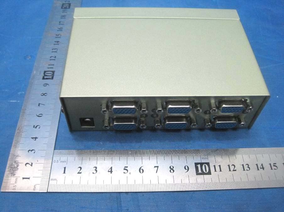
WSQMVSSERIES
Apr 11, 2010SWITCH VIDEO SPLITTER
Equipment Class
JBP - Part 15 Class B Computing Device Peripheral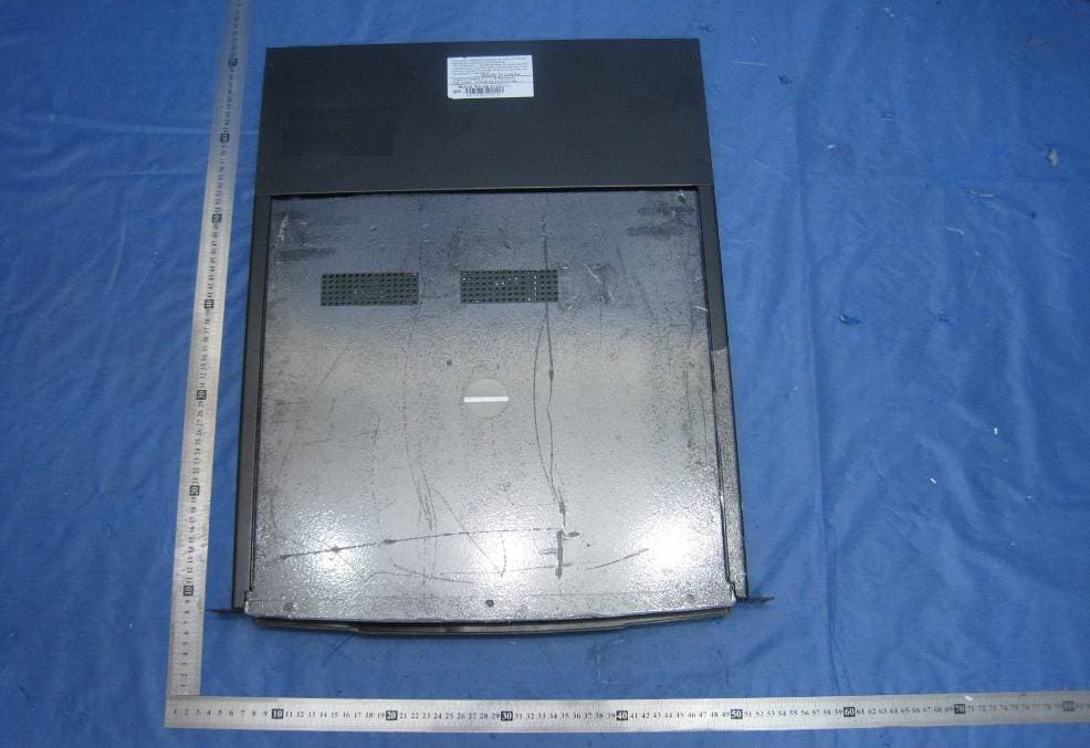
WSQAS-9116RDL
Feb 03, 2010LCD KVM
Equipment Class
JBP - Part 15 Class B Computing Device Peripheral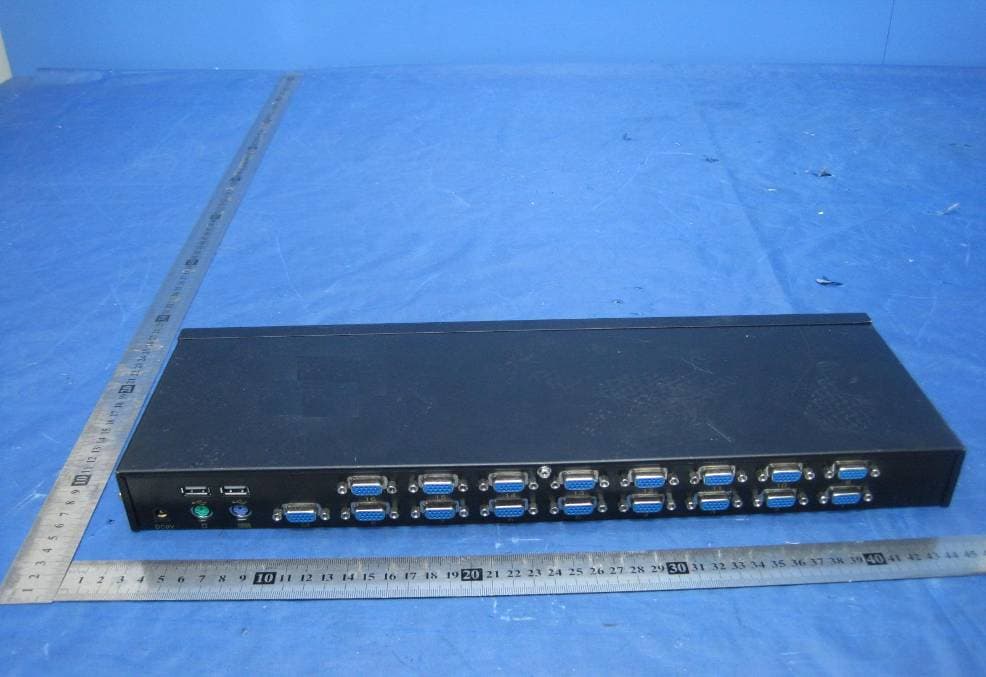
WSQAS-3116DU
Feb 01, 2010KVM SWITCH
Equipment Class
JBP - Part 15 Class B Computing Device Peripheral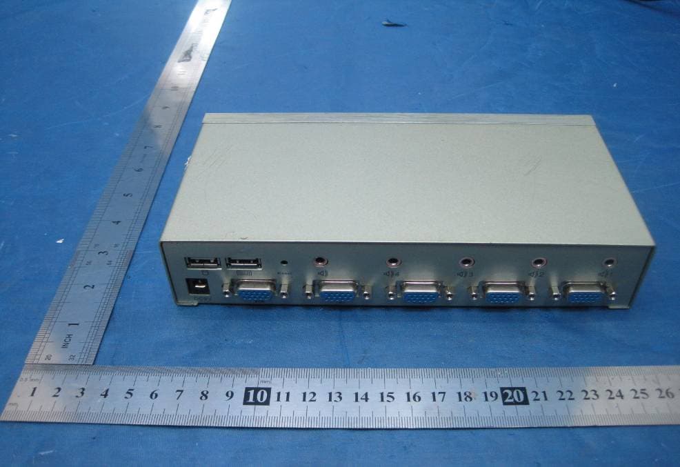
WSQAS-41P
Jan 28, 2010KVM SWITCH
Equipment Class
JBP - Part 15 Class B Computing Device Peripheral