WSQMVSSERIESSWITCH VIDEO SPLITTER
Beijing Lanbe Tianhe Technoloiges & Develop CO., Ltd.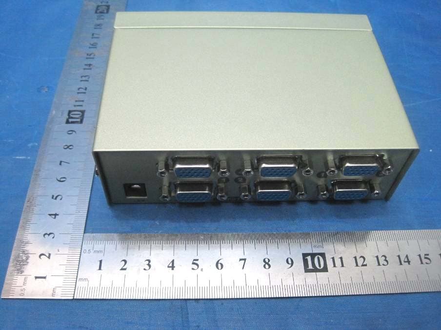
Click to zoom
Application Details
- Equipment Class
- JBP - Part 15 Class B Computing Device Peripheral
- Date of Grant
- Apr 11, 2010
- Application Purpose
- Original Equipment
- Date of Application
- Apr 11, 2010
- Equipment Note
- SWITCH VIDEO SPLITTER
- Frequency Range
- 0.04200000 - 0.04200000
- Country
- China
Documents & Files
Document Text
Text extracted from the exhibit documents filed with the FCC. Open a document above to read the original.
Users Manual
Made in China 08/01 MVS201/MVS202 / MVS204 Factory: ISO9002 System Certified Product:CCC CE FCC Certified MVS401 / MVS402 User Manual Welcome to use LANBE serial product User Manual : PRODUCT INTRODUCTION MVS201 ( 202 / 204 ) / MVS401 ( 402 ) video switch and splitter is a kind of device which can switch 2 (MVS202 / MVS204) or 4(MVS401 / MVS402) input video signals to 1/2/4 output video signals. The device is an active device. It amplifies and rectifies the output signal and ensures the high output gain, high bandwidth, high resolution and high reliability of the output signal. It can be applied in stock market, computer exhibition, movie and broadcasting company and education center etc. SAFETY GUIDE In order to make sure the device used properly and the safety of the operator, please follow the directions when installing, using and maintaining: 1. The power supply of the device is DC 9V 1000mA. 2. Do not place it in too cold or too hot environment. 3. The device heats when working. So keep the environment airy to avoid damage it by high temperature. 4. Do not try to take apart the device or repair it without permission of professionals to avoid accident. 5. Do not split any chemical or liquid on the device or near. 6. This appliance is not intended for use by persons (including children) with reduced physical, sensory or mental capabilities, or lack of experience and knowledge, unless they have been given supervision or instruction concerning use of the appliance by a person responsible for their safety. Children should be supervised to ensure that they do not play with the appliance. 7.Changes or modifications not expressly approved by the party responsible for compliance could viod the user’s authority to operate the equipment . TROUBLE SHOOTING 1 ) When no output signal, please check : A : Whether the power cable is plugged into the device. B : Whether the connection cable is damaged. C : Whether there is input signal. 2 ) If the POWER LED does not light, maybe power supply is abnormal. 3 ) If the output picture is interfered, maybe the I/O device is not grounded. 4 ) If the output picture is blurred, please check whether the connection cable has problem. SPECIFICATION Signal Type VGA Connection Type VGA 15HDF Minimum input level positive 0.5Vp-p Maximum input level positive 1.0Vp-p Video Input/Output Signal I/O Impedance 75 Ω Maximum Resolution 1920*1440 Horizontal Frequency 30-100KHz Vertical Frequency 40-120Hz Video Bandwidth 250MHz Maximum Transmission 60 meters Resolution 800*600 Distance 60HZ Power Input Voltage AC100~230V Device Input Power DC 9V/1000mA Size ( L*W*H ) 72mm*120mm*29mm Specification Weight 400g Operation Panel Shell Metal This device complies with Part 15 of the FCC Rules. FCC NOTE: This device complies with Part 15 of the FCC Rules. Operation is subject to the following two conditions:(1)this device may not cause harmful interference, and (2) this device must accept any interfere nce received, including interference that may cause undesired operation. This equipment has been tested and found to comply with the limits for a Class B digital device, pursuant to Part 15 of the FCC Rules. These limits are designed to provide reasonable protection against harmful interference in a residential installation. This equipment generates, uses and can radiate radio frequency energy and, if not installe d and used in accordance with the instructions, may cause ha rmful interference to radi o communications. However, there is no guarantee that interference will not occur in a particular installation. If this equipment does cause harmful interference to radio or television reception, which can be determined by turning the equipment off and on, the user is encouraged to try to correct the interference by one or more of the following measures: -- Reorient or relocate the receiving antenna -- Increase the separation between the equipment and receiver. -- Connect the equipment into an outlet on a circuit different from that to which the receiver is connected. -- Consult the dealer or an experien ced radio/TV technician for help.
Block Diagram
VGA Signal Input 3 multi-way stitch Power Supply VGA Signal Output 2 Computer 3 operational amplifier 2 Computer 4 VGA Signal Input 4 operational amplifier Computer 2 Computer 1 VGA Signal Input 2 VGA Signal Input 1 operational amplifier 1 VGA Signal Output 1 Working frequency 42KHz
Cover Letter(s)
FCC ID: WSQMVSSERIES POWER OF ATTORNEY January 25, 2010 Federal Communications Commission Authorization and Evaluation Division 7435 Oakland Mills Road Columbia, MD 21046 To Whom It May Concern: We, the undersigned, hereby authorize Waltek Services (ShenZhen) Co., Ltd. (Philo Zhong) on our behalf, to apply to the Federal Communications Commission on our equipment. Any and all acts carried out by Waltek Services (ShenZhen) Co., Ltd. (Philo Zhong) on our behalf shall have the same effect as acts of our own. This authorization expires on January 24,2011 This is to advise that we are in full compliance with the Anti-Drug Abuse Act. We, Beijing Lanbe Tianhe Technologies&Develop CO., Ltd.are not subject to a denial of federal benefits pursuant to Section 5301 of the Anti-Drug Act of 1988, 21 USC853a, and no party to the application is subject to a denial of federal benefits pursuant to that section. Sincerely, Beijing Lanbe Tianhe Technologies&Develop CO., Ltd. .................................... Manager
External Photos
EUT(MVS-402) - Front View EUT(MVS-402) - Back View
External Photos
FCC ID Label Sample for Model: MVS-201, MVS-202, MVS-204, MVS-401, MVS-402 FCC ID: WSQMVSSERIES This device complies with Part 15 of the FCC Rules. Operation is subject to the following two conditions: (1)this device may not cause harmful interference, and (2) this device must accept any interference received, including interference that may cause undesired operation.
ID Label/Location Info
FCC ID Label This device complies with Part 15 of the FCC Rules. Operation is subject to the following two conditions:(1)this device may not cause harmful interference, and (2) this device must accept any interference received, including interference that may cause undesired operation. The Label must not be a stick-on paper. The Label on these products must be permanently affixed to the product and readily visible at the time of purchase and must last the expected lifetime of the equipment not be readily detachable. Proposed Label Location on EUT EUT Top View/ proposed FCC Label Location FCC ID: WSQMVSSERIES This device complies with Part 15 of the FCC Rules. Operation is subject to the following two conditions:(1)this device may not cause harmful interference,and (2) this device must accept any interference received, including interference that may cause undesired operation.
Internal Photos
EUT(MVS-402)-PCB 1 -Front View EUT(MVS-402)-PCB 1 - Back View EUT(MVS-402)-PCB 2 -Front View EUT(MVS-402)-PCB 2-Back View
Operational Description
Circuit Description VGA splitter circuit description: VGA is the distributor will enter the realization of a single VGA signals or VGA display screen into multiple distribution of the same signal to reach the screen or a multi-screen display. And the working frequency is 42KHz. VGA splitter is the VGA input signal is divided into three color signals and signal field trip alone signal amplification to enhance the quality of its signal. Integrated operational amplifier to enter the R, G, B zoom, adjust its bandwidth after another output impedance matching to multiple. And then after a field trip to buffer signals, signals in the buffer, to enlarge and improve the quality of the output signal to the multi-channel. As the VGA signal through the amplification, and signal to match the buffer to increase the power and signal quality, so the signal through multiple distribution without signal attenuation and maintain the quality of the original show. As a result of the IC circuits used in the characteristics of whole circuit to provide positive and negative power supply voltage required to meet the normal work of the IC. Machines used metal shell material to ensure that work can be effective to external signal interference shielding.
Schematics
1234 A B C D 4 321 D C B A Title NumberRevisionSize A4 Date:30-Dec-2009Sheet of File:H:\公司产品\2009年PCB(SCH)核对\2009年PCB(SCH)核对\分配器\切换型\分配切换器\MVS402V2.1\ MVSDrawn By: 0 10 1 11 2 12 3 13 4 1 5 2 6 3 7 4 EI 5 EO 15 A 9 B 7 C 6 GS 14 U1 74LS148 SW1 SW2 SW3 SW4 R1 103 R2 103 R3 103 R4 103 VCC SEL1 SEL2 SEL3 D0 2 D1 3 D2 6 D3 7 Q0 16 Q1 15 Q2 10 Q3 9 Q0 1 Q1 14 Q2 11 Q3 8 E01 13 E23 4 U2 74LS75 A 1 B 2 C 3 E1 4 E2 5 E3 6 Y0 15 Y1 14 Y2 13 Y3 12 Y4 11 Y5 10 Y6 9 Y7 7 U3 74LS138 D1 LED D2 LED D3 LED D4 LED R6 471 VCC VCC SEL1 SEL2 SEL3 1 2 3 4 5 6 J1 CON SEL1 SEL2 SEL3 GND VCC R7 103 VCC C1 C104 C2 C104 C3 C104 VCC GND R8 103 VCC GND D6 1N4148 R5 0 R9 103 VCC PDF 文件使用 "pdfFactory Pro" 试用版本创建 www.fineprint.com.cn
Test Report
Beijing Lanbe Tianhe Technologies&Develop CO., Ltd. FCC ID: WSQMVSSERIES FCC TEST REPORT Page: 1 of 25 FCC ID : WSQMVSSERIES Applicant : Beijing Lanbe Tianhe Technologies&Develop CO., Ltd. Address : Room 508,Guoxin Building,SHOUT:Nan Rd. NO.20, Haidian District,Beijing,China Equipment Under Test (EUT) : Product Name : Switch video splitter Model No : MVS-201, MVS-202, MVS-204, MVS-401, MVS-402 Standards : FCC Part 15 Subpart B :2009 Date of Test :January 10~23,2010 Date of Issue : January 25,2010 Prepared By : Zero Zhou Reviewed By : Test Result : PASS * PERPARED BY: Waltek Services (Shenzhen) Co., Ltd. 1/F, Fukangtai Building,West Baima Rd.,Songgang Street, Baoan District, Shenzhen 518105,China Tel: +86-755-27553488 Fax: +86-755-27553868 Beijing Lanbe Tianhe Technologies&Develop CO., Ltd. FCC ID: WSQMVSSERIES Page:2 of 25 1 Test Summary Test Test RequirementTest Method Class / Severity Result Conducted Emission (150KHz to 30MHz) FCC PART 15, SUBPART B: 2009 ANSI C63.4: 2009 FCC PART15.107 PASS Radiated Emission (30MHz to 1GHz) FCC PART 15, SUBPART B: 2009 ANSI C63.4: 2009 FCC PART15.109 PASS Beijing Lanbe Tianhe Technologies&Develop CO., Ltd. FCC ID: WSQMVSSERIES Page:3 of 25 2 Contents 1 COVER PAGE ......................................................................................................................................................... 1 1 TEST SUMMARY........................................................................................................................................................ 2 2 CONTENTS............................................................................................................................................................. 3 3 GENERAL INFORMATION ................................................................................................................................ 4 3.1 CLIENT INFORMATION........................................................................................................................................... 4 3.2 GENERAL DESCRIPTION OF E.U.T. ........................................................................................................................ 4 3.3 DETAILS OF E.U.T................................................................................................................................................. 4 3.4 DESCRIPTION OF SUPPORT UNITS.......................................................................................................................... 4 3.5 STANDARDS APPLICABLE FOR TESTING................................................................................................................ 4 3.6 TEST FACILITY...................................................................................................................................................... 5 3.7 TEST LOCATION.................................................................................................................................................... 5 4 EQUIPMENT USED DURING TEST .................................................................................................................. 6 5 EMISSIONS TEST RESULTS .............................................................................................................................. 9 5.1 CONDUCTED EMISSION DATA...............................................................................................................................9 5.1.1 E.U.T. Operation ........................................................................................................................................ 9 5.1.2 EUT Setup ................................................................................................................................................... 9 5.1.3 Conducted Emission Test Data................................................................................................................. 11 5.1.4 Photograph – Conducted Emission Test Setup......................................................................................... 13 5.2 RADIATION EMISSION DATA...............................................................................................................................14 5.2.1 Measurement Uncertainty......................................................................................................................... 14 5.2.2 EUT Setup ................................................................................................................................................. 14 5.2.3 Spectrum Analyzer Setup .......................................................................................................................... 16 5.2.4 Test Procedure.......................................................................................................................................... 16 5.2.5 Corrected Amplitude & Margin Calculation ............................................................................................ 16 5.2.6 Summary of Test Results ........................................................................................................................... 17 5.2.7 Photograph – Radiation Emission Test Setup .......................................................................................... 19 6 PHOTOGRAPHS - CONSTRUCTIONAL DETAILS...................................................................................... 20 6.1 EUT(MVS-402) - FRONT VIEW.......................................................................................................................... 20 6.2 EUT(MVS-402) - BACK VIEW............................................................................................................................ 20 6.3 EUT(MVS-402)-PCB 1 -FRONT VIEW............................................................................................................... 21 6.4 EUT(MVS-402)-PCB 1 - BACK VIEW..............................................................…
Text truncated - open the document above for the full version.
Test Setup Photos
Photograph – Radiation Emission Test Setup Photograph – Conducted Emission Test Setup
Contact Information
Applicant
Li hua cui(Manager)
Test Firm
Waltek Services(Shenzhen) Co., Ltd.Philo zhong
Technical Specifications
| # | Rule Parts | Frequency Range | Power Output |
|---|---|---|---|
| 1 | 15B | 0.042 MHz - 0.042 MHz | - |
Other Applications from Beijing Lanbe Tianhe Technoloiges & Develop CO., Ltd.
WSQKSSERIES
Mar 27, 2011KVM SWITCH
Equipment Class
JBP - Part 15 Class B Computing Device Peripheral
WSQAS-9116RDL
Feb 03, 2010LCD KVM
Equipment Class
JBP - Part 15 Class B Computing Device Peripheral
WSQAS-3116DU
Feb 01, 2010KVM SWITCH
Equipment Class
JBP - Part 15 Class B Computing Device Peripheral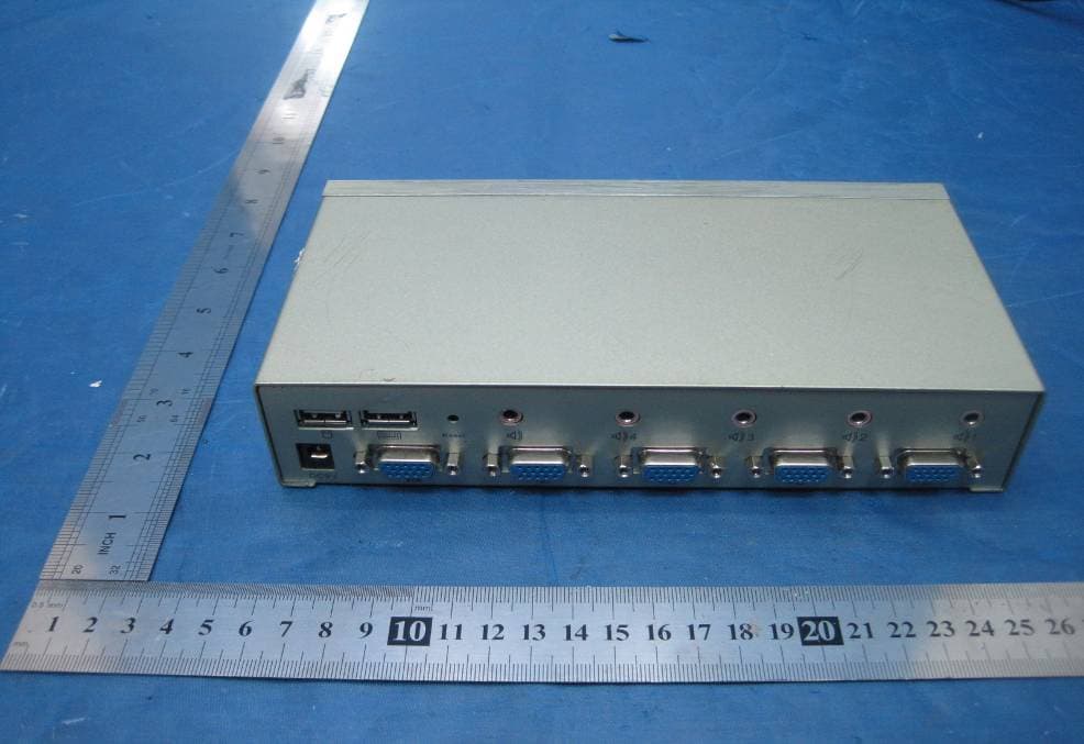
WSQAS-41P
Jan 28, 2010KVM SWITCH
Equipment Class
JBP - Part 15 Class B Computing Device Peripheral