Y9AW210AREMOTE CONTROL/SECURITY DEVICE TRANSCEIVER
SEBINE Technology, Inc.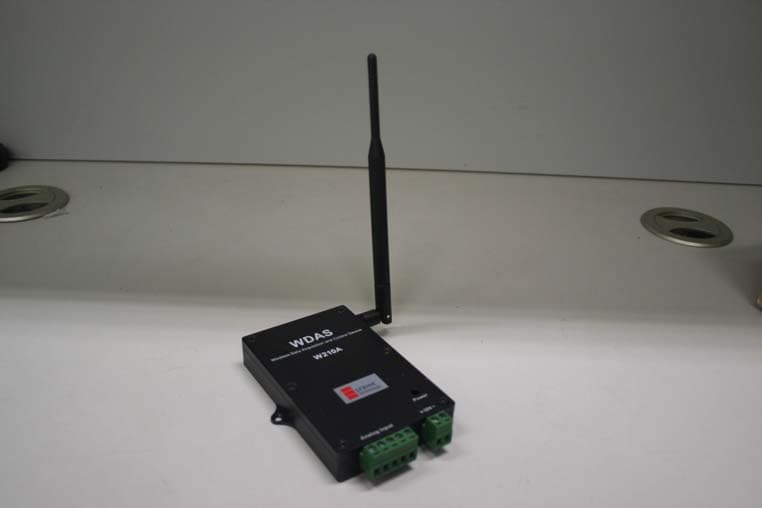
Click to zoom
Application Details
- Equipment Class
- DSR - Part 15 Remote Control/Security Device Transceiver
- Date of Grant
- Aug 03, 2011
- Application Purpose
- Original Equipment
- Date of Application
- Aug 03, 2011
- Equipment Note
- REMOTE CONTROL/SECURITY DEVICE TRANSCEIVER
- Frequency Range
- 433.06250000 - 434.76250000
- Company
- SEBINE Technology, Inc.
- Country
- South Korea
Documents & Files
Document Text
Text extracted from the exhibit documents filed with the FCC. Open a document above to read the original.
Users Manual
W210A W210A_20110725.hwp1 WDAS Wireless Data Acquisition and Control System W210A User's Manual Ver 2.0 SEBINE Technology, Inc. W210A W210A_20110725.hwp2 This device complies with Part 15 of the FCC Rules. Operation is subject to the following two conditions: (1) This device may not cause harmful interference, and (2) this device must accept any interference received, including interference that may cause undesired operation. W210A W210A_20110725.hwp3 CONTENTS 1. Summary 1.1 Product Introduction 1.2 Specification 2. Operation 2.1 PC MODE 3. Device Connection 3.1 Power Supply 3.2 Analog Input Connection 4. Environment Setup 4.1 Hardware Connection 4.2 Setup List of Each Mode 5. Examples Appendix 1. Dimension Appendix 2. R&TTE Appendix 3. Document Information W210A W210A_20110725.hwp4 1. Summary 1.1 Product Introduction W210A is one of WDAS(Wireless Data Acquisition and Control System) products and it is a wireless data transmitter-receiver which receives analog input data for controlling signal by using 433MHz RF frequency bandwidth. W210A allows users to set communication channels via environment setting. Usable frequency number, channel number, and serial number are printed in shipping products. Figure 1. W210A W210A W210A_20110725.hwp5 1.1.1 Application examples Figure 2. On/Off Status Wireless Transmission by W210A and M110A 1.1.2 Product usage lCable system replacement : Maintenance difficulty with cables is solved lHard environment for cable installation : Environment that requires long and co mplicated cable installation is solved lUneasy area for data acquisition by cable : Outdoor tank monitoring system 1.1.3 Product application area lPump, pipeline, liquid flow monitoring system lTank level, temperature monitoring system 1.1.4 Product parts W210A main body, one λ/4 dipole antenna, one power connector, one Analog Input connector W210A W210A_20110725.hwp6 ItemSpecification Name W210A Dimension 109mm(L)×85mm(W)×18.6mm(H) (w/o Antenna) Housing Aluminum Weight 150g (w/o Antenna) Power Supply +12Vdc ±10%, Reverse Power/Overvoltage/Overcurrent Protection Current Consumption Rx 80mA Tx 86mA WDT Reset 88mA (@12Vdc) Operating Temperature -10°C ~ +60°C RF Features • Frequency : 433.0625MHz ~ 434.7625MHz • Channel Spacing : 25KHz • Transmitter Power : 73dBuV/m • Receiver Sensitivity : -116 ~ -120dBm(-116dBm typ.) • Modulation : FSK • Bandwidth : < 14KHz Performance • Expected Line-Of-Sight Range : Up To 1.5km with λ/4 Dipole Antenna • RF Data Rate : 4.8K Baud, 7.2K Baud I/O Interface Analog Input 2Ch. Analog Input, with 16Bit Resolution (0~5V, 0~10V, 4~20mA) User Selectable Input Type : Current or Voltage User Selectable Input Voltage Range : 0~5V or 0~10V Antenna Interface • SMA(Female, Reverse)Connector • Impedance 50Ω 1.2 Specification Table 1. W210A Specification W210A W210A_20110725.hwp7 2. Operation W210A can use only PC MODE. Refer the Programmer guide for detailed protocol and Function Code. 2.1 PC MODE 2.1.1 Definition of PC MODE Through M110A(PC MODE), W110A(Only PC MODE) with serial port, W210A execute the command when valid Function Code is received. - Valid receiver Function Code : READ Figure 3. PC MODE of W210A 2.1.2 Function Code available at PC MODE - READ : Through M110A(PC MODE), W110A(Only PC MODE) with serial port, current analog input status is read when W210A receives Function Code of inquiry of analog input status. - READ_RESPONSE : Function Code of READ_RESPONSE is used when READ Function Code is received and current analog input status is transmitted. 2.1.3 Environment setting list before PC MODE use - Non W210A W210A_20110725.hwp8 3. Device Connection Figure 5. W210A Outer Figure 6. W210A Inner W210A W210A_20110725.hwp9 3.1 Power Supply W210A works at +12Vdc and equipped with Reverse Power / Overvoltage / Overcurrent Protection circuitry. Power is supplied by power connector provided at product purchase as shown in figure below. W210A has no external power switch and it becomes in working mode when the power is supplied. If normal power is supplied, power supply indicator LED is on. As shown in Figure 7, remove the skin of wire about 7mm and put it into the terminal and tighten it by turning the left screw using screwdriver. As shown in Figure 8, connect it to power. As shown in Figure 9, connect the terminal to power port of W210A, Make sure the direction is exact as shown in Figure 9. Figure7. Power Supply-1 Figure8. Power Supply-2 Figure9. Power Supply-3 ※ Notice Readily accessible disconnect device shall be incorporated external to the equipment. W210A W210A_20110725.hwp10 3.2 Analog Input Connection and Setting W210A supports 2 input channel. For analog input function, use Analog Input connector in Figure 10. Analog Input connector is included in product purchase. Connection method is same as power supply connection method. Figure 10. W210A connector 3.2.1 Analog input connection Analog input channel generates input via the difference between AGND and corresponding analog input channel pins. Thus, the both ends of device that generates analog input should be connected to corresponding channel pins and AGND. 3.2.2 Analog input channel setup For use of anlog input, AI#0 voltage input level setting jumper, AI#1 voltage input level setting jumper, AI#0 voltage/current input setting jumper, AI#1 voltage/current input setting jumper adjustments are needed as shown in Figure 11. W210A W210A_20110725.hwp11 Figure 11. W210A analog input channel setting concept AI#0 : AI#0 can select voltage/current input receipt. When receiving voltage, set the jumper of J8 as V and adjust the voltage input range, then receive voltage via pin 1 of Analog Input connector. When receiving current, set the jumper of J6 as C, then receive current via pin 4 of analog input connector. AI#1 : AI#1 can select voltage/current input receipt. When receiving voltage, set the jumper of J9 as V and adjust the voltage input range, then receive voltage via pin 2 of Analog Input connector. When r…
Text truncated - open the document above for the full version.
Cover Letter(s)
Date : July 4, 2011 To Whom it may concern : We the undersigned, here by authorize CHUNGBUK TECHNOPARK. to act as our authorized agent on our behalf in all manners relating to application for FCC equipment authorization. including signing of all documents relating to these matters. Any individual within this entity may act on our behalf. Any and all acts carried out by CHUNGBUK TECHNOPARK. On our behalf shall have the same effect as acts of our own. This authorization is valid until further written notice from SEBINE Technology, Inc. Sincerely, Signature Eun-Seong, Yoo Manager of Development Team SEBINE Technology, Inc.
Cover Letter(s)
CHUNGBUK TECHNOPARK #685-3, Yangcheong, Ochang, Cheongwon, Chungbuk, Korea TEL:+82-43-270-2400 FAX:+82-43-270-2499 http://www.cbtp.or.kr Date : July 4, 2011 Federal Communications Commission Authorization and Evaluation Division Confidentiality Request regarding application for certification ofFCC ID: Y9AW210A Pursuant to Sections 0.457 and 0.459 of the Commission’s Rules, we hereby request confidential treatment of informationaccompanying this application as outlined below: Block Diagram Schematics Part list Operational Description The above materials contain trade secrets and proprietary information not customarily released to the public. The public disclosure of these materials may be harmful to the applicant and provide unjustified benefits to its competitors. The applicant understands that pursuant to Section 0.457 of the Rules, disclosure of this application and all accompanying documentation will not be made before the date of the Grant for this application. Sincerely, Signature Kook-Sun, Shin Chief Engineer of Convergence Parts Team CHUNGBUK TECHNOPARK
External Photos
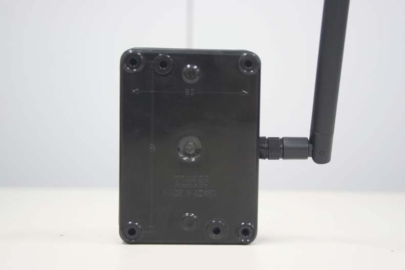
CHUNGBUK TECHNOPARK #685-3, Yangcheong, Ochang, Cheongwon, Chungbuk, Korea TEL:+82-43-270-2400 FAX:+82-43-270-2499 http://www.cbtp.or.kr Report Number : CBTP-11R-0015Page: 27/28 This report may not be reproduced without the full written approval of CHUNGBUK TECHNOPARK. 13. Photographs of Equipment Under Test(EUT) [Front View] [Rear View]
ID Label/Location Info
CHUNGBUK TECHNOPARK #685-3, Yangcheong, Ochang, Cheongwon, Chungbuk, Korea TEL:+82-43-270-2400 FAX:+82-43-270-2499 http://www.cbtp.or.kr Report Number : CBTP-11R-0015Page: 23/28 This report may not be reproduced without the full written approval of CHUNGBUK TECHNOPARK. 9. FCC Labelling Requirements 9.1 FCC Statement Product shall be labelled the following statement in the manual: This device complies with Part 15 of the FCC Rules. Operation is subject to the following two conditions: (1) This device may not cause harmful interference, and (2) this device must accept any interference received, including interference that may cause undesired operation. When the device is so small or for such use that it is not practicable to place the statement on it, the information shall be placed in prominent location in theinstruction manual or pamphlet supplied to the user. However, the FCC identifier or unique identifier, as appropriate, must be displayed on the device. CHUNGBUK TECHNOPARK #685-3, Yangcheong, Ochang, Cheongwon, Chungbuk, Korea TEL:+82-43-270-2400 FAX:+82-43-270-2499 http://www.cbtp.or.kr Report Number : CBTP-11R-0015Page: 24/28 This report may not be reproduced without the full written approval of CHUNGBUK TECHNOPARK. 9.2 Label & Label Location SEBINE Technology, Inc. Model : W210A FCCID:Y9AW210A Made in Korea
Internal Photos
DBG port for PC MODE
Internal Photos
CHUNGBUK TECHNOPARK #685-3, Yangcheong, Ochang, Cheongwon, Chungbuk, Korea TEL:+82-43-270-2400 FAX:+82-43-270-2499 http://www.cbtp.or.kr Report Number : CBTP-11R-0015Page: 28/28 This report may not be reproduced without the full written approval of CHUNGBUK TECHNOPARK. [Internal Photograph]
RF Exposure Info
사양 승인원 (Approval Sheet) 프로젝트 명(PROJECT NAME) WHIP Anrenna 도 번(MODEL No.) HS9-433-SW Rev.IR 품목번호(ITEM No.) HS9-433-SW 세빈기술 기구 (MECHANIC) 담 당 검 토 승 인 전자 (ELECTRONIC) 담 당 검 토 승 인 혜성전자통신 기구 (MECHANIC) 담 당 검 토 승 인 전자 (ELECTRONIC) 담 당 검 토 승 인 2009년 10 월 19 일 경기도 시흥시 하상동 377-4 ‡ 429 - 270 혜 성 전 자 통 신 대표 이 호 수 (인) Date 2009. 10. 19 Version No. 1.0 Subject HS9-433-SW 2/13 HYESUNG CO. 목 차 (Table of Contents) 1. 승인원 이력 LIST(Approval Sheet Check List) .............................................................. 3 2. 개 요(APPLICATION) .................................................................................................. 4 2.1. 개요 ......................................................................................................................................................... 4 3. 규 격(Specification) ....................................................................................................... 5 3.1. 일반 규격 ................................................................................................................................................. 5 3.2. 전기적 규격 ............................................................................................................................................. 5 3.3. 기계적 규격 ............................................................................................................................................. 5 4. 시험방법 및 절차서(Test Procedure & Measurement) ................................................... 6 4.1. 외관검사 ................................................................................................................................................... 6 4.2. 전기적 특성검사 ...................................................................................................................................... 6 4.2.1. 준비물 ............................................................................................................. 6 4.2.2. 검사 ................................................................................................................ 6 5. 포장 및 운반(Packing, Shipping, Handling) .................................................................... 8 5.1. 외관사양 ................................................................................................................................................... 8 5.2. 포 장 ................................................................................................................................................... 8 6. 외 관(Appearance) ........................................................................................................... 9 7. 시험성적서(Test Data Sheet) ........................................................................................... 10 8. Data Sheet ......................................................................................................................... 11 8.1. V.S.W.R .................................................................................................................................................. 11 8.2. Impedance ...................................................................... 오류! 책갈피가 정의되어 있지 않습니다. 8.3. Gain Patterns ................................................................. 오류! 책갈피가 정의되어 있지 않습니다. 8.3.1 Azimuth Patterns ................................................... 오류! 책갈피가 정의되어 있지 않습니다. 8.3.2 Elevation Patterns ............................................ 오류! 책갈피가 정의되어 있지 않습니다. Date 2009. 10. 19 Version No. 1.0 Subject HS9-433-SW 3/13 HYESUNG CO. 1. 승인원 이력 LIST(Approval Sheet Check List) 이 력 변 경 날 짜 항 목 / 내 용 근 거 승인원 issue 제품 issue Ver 1.0 Ver 1.0 2009.10.19 초도승인 세빈기술 Date 2009. 10. 19 Version No. 1.0 Subject HS9-433-SW 4/13 HYESUNG CO. 2. 개 요(APPLICATION) 2.1. 개요 본 규격서는 HS9-433-SW의 사양에 대해 기술하였다. Date 2009. 10. 19 Version No. 1.0 Subject HS9-433-SW 5/13 HYESUNG CO. 3. 규 격(Specification) 3.1. 일반 규격 General specification Model name HS9-433-SW Antenna type WHIP Antenna 3.2. 전기적 규격 Electrical specification Frequency range 433㎒ V.S.W.R 1.9: 1 Max. Gain(dBi) 2±0.5 Radiation pattern Omni-directional Polarization Vertical Max Power(W) 5W Max. Impedance 50 Ω Normalizer 3.3. 기계적 규격 Mechanical specification Connector type SMA(M) Cover material Keyfiex Color BLACK Temperature range -30°C ~ 70°C Weight 12 ± 0.2g Dimension TBD Date 2009. 10. 19 Version No. 1.0 Subject HS9-433-SW 6/13 HYESUNG CO. 4. 시험방법 및 절차서(Test Procedure & Measurement) 4.1. 외관검사 Antenna의 외관 및 치수, Connector등이 첨부된 “ 6 ” 번 항의 외관과 일치 하는지를 확인한다. 4.2. 전기적 특성검사 4.2.1. 준비물 장 비 명 Model 수량규 격 Network Analyzer HP8753E (또는 동등 이상의 장비) 1대 · Freq. Range : 300KHz ~ 3GHz · Accuracy : <5ppm · Dynamic Range : 105dB · Trace at ±200dB · Resolution : 1Hz · Impedance : 50 Ω Adaptor 1EA· N(M) Calibration Kit HP85032B 1Set · DC ~ 6GHz (N-Type) 4.2.2. 검사 그림 1. Network Analyzer 검사 시 계측기 연결도 PRINTER Date 2009. 10. 19 Version No. 1.0 Subject HS9-433-SW 7/13 HYESUNG CO. 4.2.2.1. 검사 가. 장비 Setting 및 Calibration ㉠ 장비 Setting ⓐ 주파수대역 : Center Frequency: 433MHz, Span :100.0MHz ⓑ Source Power : 10dBm, ⓒ IF Bandwidth : 1000Hz ⓓ Number of Point : 401 ㉡ Calibration N-Type Cal. Kit을 사용하여 O.S.L 방법으로 1 Port Calibration한다. ⓐ S 11 Calibration : Port 1에 Open, Short, Load를 각각 연결하여 Calibration한다. ㉢ Calibration 확인 ⓐ Port1에 Load를 연결하여 S 11 의 V.S.W.R이 1.02 : 1이하 인지를 확인한다. ⓑ Port1에 Load를 연결하여 S 21 값이 – 80.0dB 이하인지를 확인한다. 확인 결과 위의 기준을 만족하지 못할 경우 ㉡항의 Calibration 항을 반복 수행한다. 나. 검사방법 및 내용 항 목 검 사 방 법 기 준 VSWR 위 그림 1과 같이, ANT에 Network Analyzer의 Port 1을 연결한 다음 Operating Band 내에서의 S 11 값을 측정한다. 1.9:1 Max. Impedance 위 그림 1과 같이, ANT에 Network Analyzer의 Port 1을 연결한 다음 Operating Band 내에서의 Smith Chart 상의 S 11 값을 측정한다. 50 ± 20Ω Date 2009. 10. 19 Version No. 1.0 Subject HS9-433-SW 8/13 HYESUNG CO. 5. 포장 및 운반(Packing, Shipping, Handling) 5.1. 외관사양 가. 주문자의 상호와 생산자의 상호가 명기되어야 한다. 나. Model 명 및 수량이 명기되어야 한다. 5.2. 포 장 가. 본 제품의 보관 및 수송에 따른 진동, 충격으로부터 보호 될 수 있도록 안전하게 포장한다. 나. 포장재료는 종이박스(HS 1종)로 하되, 제품에 손상이 가지 않는 재질을 이용한다. Date 2009. 10. 19 Version No. 1.0 Subject HS9-433-SW 9/13 HYESUNG CO. 6. 외 관(Appeara…
Text truncated - open the document above for the full version.
Test Report
CHUNGBUK TECHNOPARK #685-3, Yangcheong, Ochang, Cheongwon, Chungbuk, Korea TEL:+82-43-270-2400 FAX:+82-43-270-2499 http://www.cbtp.or.kr Report Number : CBTP-11R-0015Page: 1/30 This report may not be reproduced without the full written approval of CHUNGBUK TECHNOPARK. TEST REPORT FCC PART 15 C Applicant Trade Name SEBINE Technology, Inc. Address RN 202, Daedeok Radio Engineering Center, 604. Tamnip-dong, Yuseong-gu, Daejeon, Korea 305-510 Telephone Number 82-42-935-2085Fax Number82-42-935-2088 Product Name WDAS Model Name W210A Manufacturer SEBINE Technology, Inc. Test Date2011.4. 25. ~ 2011.7. 21. Issued Date2011.7. 25. Test ProcedureANSI C63.4-2003 Applicable RegulationFCC Part 15.231 FCC IDY9AW210A FCC ClassificationDSR / Part 15 Remote Control/Security Device Transceiver Test ResultPass■Fail□ Test EngineerChief Engineer Eunjung, YangKook-Sun, Shin CHUNGBUK TECHNOPARK I, the undersigned, hereby declare that the equipment specified aboveconforms to the above FCC Rule(s) and Regulation(s) Part 15 as described in the attached test report. This test report contains only the result of a single test of the sample supplied for the examination. CHUNGBUK TECHNOPARK #685-3, Yangcheong, Ochang, Cheongwon, Chungbuk, Korea TEL:+82-43-270-2400 FAX:+82-43-270-2499 http://www.cbtp.or.kr Report Number : CBTP-11R-0015Page: 2/30 This report may not be reproduced without the full written approval of CHUNGBUK TECHNOPARK. TABLE OF CONTENTS 1. Test Laboratory ······················································································································· 3 1.1 General Information ········································································································································ 3 1.2 Location of Test Laboratory ························································································································· 3 1.3 Registration Information ································································································································· 3 2. Test Rule ································································································································· 4 2.1 Test Rule Part(s) ············································································································································ 4 2.2 Equipment Under Test(EUT) Modifications ································································································ 4 3. Description for Equipment Under Test(EUT) ····································································· 5 4. Test Equipment ······················································································································· 6 5. Transmission time & Silent time ························································································· 7 6. Field strength of fundamental ····························································································· 12 7. Field strength of the spurious emissions & Radiated emissions ···································· 13 8. 20 dB bandwidth ·················································································································· 22 9. FCC Labelling Requirements ······························································································ 25 10. Test Setup Photographs ······································································································ 27 11. Photographs of Equipment Under Test(EUT) ································································· 29 CHUNGBUK TECHNOPARK #685-3, Yangcheong, Ochang, Cheongwon, Chungbuk, Korea TEL:+82-43-270-2400 FAX:+82-43-270-2499 http://www.cbtp.or.kr Report Number : CBTP-11R-0015Page: 3/30 This report may not be reproduced without the full written approval of CHUNGBUK TECHNOPARK. 1. Test Laboratory 1.1 General Information Name of LaboratoryCHUNGBUK TECHNOPARK RepresentativeJongsung, Lim Address 685-1 Yangcheong-ri, Ochang-eup, Cheongwon-gun, Chungcheongbuk-do, Korea Telephone Number+82-43-270-2000 Fax Number+82-43-270-2099 Homepagewww.cbtp.or.kr 1.2 Location of Test Laboratory Address 685-3 Yangcheong-ri, Ochang-eup, Cheongwon-gun, Chungcheongbuk-do, Korea Telephone Number+82-43-270-2400 Fax Number+82-43-270-2499 1.3 Registration Information Test item(s)FacilityRegistration Number Radiated Emission Measurement10m semi-anechoic chamber 647924 Conducted Emission MeasurementShielded room CHUNGBUK TECHNOPARK #685-3, Yangcheong, Ochang, Cheongwon, Chungbuk, Korea TEL:+82-43-270-2400 FAX:+82-43-270-2499 http://www.cbtp.or.kr Report Number : CBTP-11R-0015Page: 4/30 This report may not be reproduced without the full written approval of CHUNGBUK TECHNOPARK. 2. Test Rule 2.1 Test Rule Part(s) Test item(s)Test Rule Part(s)Test Result 1. Transmission time & silent time15.231 (e) Pass■Fail□ 2. Field strength of fundamental15.231 (e) Pass■Fail□ 3. Field strength of the spurious emissions & Radiated emissions 15.231 (e) 15.231 (b) 15.209 15.205 Pass■Fail□ 4. 20 dB bandwidth15.231 (c) Pass■Fail□ 2.2 Equipment Under Test(EUT) Modifications No modifications were made to the EUT in order to achieve and maintain compliance to the standards described in this report. CHUNGBUK TECHNOPARK #685-3, Yangcheong, Ochang, Cheongwon, Chungbuk, Korea TEL:+82-43-270-2400 FAX:+82-43-270-2499 http://www.cbtp.or.kr Report Number : CBTP-11R-0015Page: 5/30 This report may not be reproduced without the full written approval of CHUNGBUK TECHNOPARK. 3. Description for Equipment Under Test(EUT) CHUNGBUK TECHNOPARK #685-3, Yangcheong, Ochang, Cheongwon, Chungbuk, Korea TEL:+82-43-270-2400 FAX:+82-43-270-2499 http://www.cbtp.or.kr Report Number : CBTP-11R-0015Page: 6/30 This report may not be reproduced without the full written approval of CHUNGBUK TECHNOPARK. 4. TEST EQUIPMENT 4.1 Operation of Equipment Under Test(EUT) The Equipment Under Test was configured for …
Text truncated - open the document above for the full version.
Test Setup Photos
CHUNGBUK TECHNOPARK #685-3, Yangcheong, Ochang, Cheongwon, Chungbuk, Korea TEL:+82-43-270-2400 FAX:+82-43-270-2499 http://www.cbtp.or.kr Report Number : CBTP-11R-0015Page: 25/28 This report may not be reproduced without the full written approval of CHUNGBUK TECHNOPARK. 12. Test Setup Photographs 12.1 Radiated Emission Measurement, 30 MHz to 1000 MHz [Front View] [Rear View] CHUNGBUK TECHNOPARK #685-3, Yangcheong, Ochang, Cheongwon, Chungbuk, Korea TEL:+82-43-270-2400 FAX:+82-43-270-2499 http://www.cbtp.or.kr Report Number : CBTP-11R-0015Page: 26/28 This report may not be reproduced without the full written approval of CHUNGBUK TECHNOPARK. 12.2 Radiated Emission Measurement, 1.0 GHz to 5.0 GHz [Front View] [Rear View]
Contact Information
Applicant
Eun-Seong Yoo(Manager)
Test Firm
CHUNGBUK TECHNOPARKSeong-Uk Park
Technical Specifications
| # | Rule Parts | Frequency Range | Power Output |
|---|---|---|---|
| 1 | 15.231 | 433.0625 MHz - 434.7625 MHz | - |
Other Applications from SEBINE Technology, Inc.
Y9AWTH
Feb 01, 2012WTH
Equipment Class
DTS - Digital Transmission System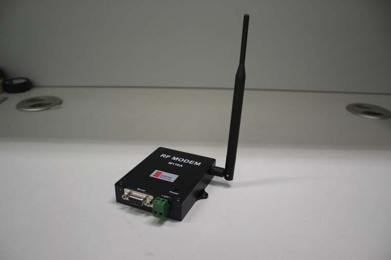
Y9AM110A
Aug 03, 2011RF MODEM
Equipment Class
JBP - Part 15 Class B Computing Device Peripheral