YAMX1EVHFDMR Convert Radio
Hytera Communications Corporation Limited
Click to zoom
Application Details
- Equipment Class
- DSS - Part 15 Spread Spectrum Transmitter
- Date of Grant
- May 07, 2012
- Application Purpose
- Original Equipment
- Date of Application
- May 07, 2012
- Equipment Note
- DMR Convert Radio
- Frequency Range
- 2402.00000000 - 2480.00000000
- Country
- China
Documents & Files
Document Text
Text extracted from the exhibit documents filed with the FCC. Open a document above to read the original.
Users Manual
Preface Thanks for your favor in our product. To derive optimum performance from the product, please read this manual and the supplied Safety Information Booklet carefully before use. This manual is applicable to the following model: X1e Instructional Icons The radio is not intended for use by general population in an uncontrolled environment. It is only for occupational use and only applied to work-related conditions. The radio must be only used by users, who are fully aware of the hazards of the exposure and who are able to exercise control over their RF exposure to qualify for the higher exposure limits. The following icons are available through this manual: Alert Icons Caution: indicates situations that could cause damage to your product. Note: indicates tips that can help you make better use of your product. Function Icons : indicates functions that are available on digital channel only. : indicates functions that are available on analog channel only. Functions marked with no function icons are available on both analog and digital channels. Term Explanation Key Operation Short press: to press a key and release it quickly. Long press: to press a key and remain holding it down for a predefined period (2 seconds by default). Hold down: to press a key and remain holding it down. Private Call Private Call is a call initiated by a single user to another user. Group Call Group Call is a call initiated by a single user to a group. All Call All Call is a call initiated by a single user to all the other users on a channel. Squelch This technology can remove excessive background noises, improving your communication quality. Copyright Information Hytera is the trademark or registered trademark of Hytera Communications Co., Ltd. (the Company) in PRC and/or other countries or areas. The Company retains the ownership of its trademarks and product names. All other trademarks and/or product names that may be used in this manual are properties of their respective owners. The product described in this manual may include the Company’s computer programs stored in memory or other media. Laws in PRC and/or other countries or areas protect the exclusive rights of the Company with respect to its computer programs. The purchase of this product shall not be deemed to grant, either directly or by implication, any rights to the purchaser regarding the Company’s computer programs. Any of the Company’s computer programs may not be copied, modified, distributed, decompiled, or reverse-engineered in any manner without the prior written consent of the Company. The AMBE+2 TM voice coding technology embodied in this product is protected by intellectual property rights including patent rights, copyrights and trade secrets of Digital Voice Systems, Inc. This voice coding technology is licensed solely for use within this product. The user of this technology is explicitly prohibited from attempting to decompile, reverse engineer, or disassemble the Object Code or in any other way convert the Object Code into a human readable form. U.S. Patent Nos. #6,912,495 B2, #6,199,037 B1, #5,870,405, #5,826,222, #5,754,974, #5,701,390, #5,715,365, #5,649,050, #5,630,011, #5,581,656, #5,517,511, #5,491,772, #5,247,579, #5,226,084 and #5,195,166. Disclaimer The Company endeavors to achieve the accuracy and completeness of this manual, but no warranty of accuracy or reliability is given. All the specifications and designs are subject to change without notice due to continuous technology development. No part of this manual may be copied, modified, translated, or distributed in any manner without the express written permission of us. If you have any suggestions or would like to learn more details, please visit our website at: http://www.hytera.com. RF Radiation Information RF Radiation Profile Radio Frequency (RF) is a frequency of electromagnetic radiation in the range at which radio signals are transmitted. RF technology is widely used in communication, medicine, food processing and other fields. It may generate radiation during use. RF Radiation Safety In order to ensure user health, experts from relevant industries including science, engineering, medicine and health work with international organizations to develop standards for safe exposure to RF radiation. These standards consist of: ●United States Federal Communications Commission, Code of Federal Regulations; 47CFR part 2 sub-part J; ● American National Standards Institute (ANSI)/Institute of Electrical and Electronic Engineers (IEEE) C95. 1-1992; ● Institute of Electrical and Electronic Engineers (IEEE) C95. 1 – 1999; ●International Commission on Non-Ionizing Radiation Protection (ICNIRP) 1998; FCC Regulations Federal Communication Commission (FCC) requires that all radio communication products should meet the requirements set forth in the above standards before they can be marketed in the U.S, and the manufacturer shall post a RF label on the product to inform users of operational instructions, so as to enhance their occupational health against exposure to RF energy. Operational Instructions and Training Guidelines To ensure optimal performance and compliance with the occupational/controlled environment RF energy exposure limits in the above standards and guidelines, users should transmit no more than 50% of the time and always adhere to the following procedures: Your radio radiates measurable RF energy only while it is transmitting (during talking), not when it is receiving (listening) or in standby mode. FCC Statement This equipment has been tested and found to comply with the limits for a Class B digital device, pursuant to part 15 of FCC Rules. These limits are designed to provide reasonable protection against harmful interference in a residential installation. This equipment generates and can radiate radio frequency energy and, if not installed and used in accordance with the instructions, may cause harmful interference to radio communications. However, there is no guarante…
Text truncated - open the document above for the full version.
Block Diagram
Pre-Drive2Drive-stage Final-stage Tx/Rx Switch Low-pass Filter Tx_VCO AD9864 Frequency Synthesizer Rx_VCO Band-pass Filter1 Low-Noise Amp Band-pass Filter2 Mixer IF FilterIF ProcessorIF Amp Ref. Osc 19.2MHZ . MOD1 MOD2+Freq error shift OMAP 4CH DAC GPS module BPF HPF ANT Microstrip Matcher TV1/APC LPF RX/TX VCO amplifier TO omap TV1 /APC From OMAP TV1/APC Reference OSC signal CV Buffer Pi Attenuator 1 2 BATT+ Stop band filter Adapt SW Adapt control APC module Low-Noise Amp OP Pre-driver1 RX/TX VCO buffer LPF LPF Pi Attenuator 1 2 CV SW CV-read control CV out 1 2 Pi Attenuator Pi Attenuator BT Module BT ANT LDO: 5V LDO:5V DC to DC 600mA DC to DC 600mA 15mA/3V3D RF PA 7.4V/1.6A RQA0002DNS Vcc1 /2 2.2V-18V 210mA/Po=0.89W/7.4V AF PA(TDA8547TS) DVDD 1.65V-1.8V-1.95V Digital core IOVDD 2V- 3.6V(MCLK=100M)I/O 2V- 3.6V(MCLK=50M) 1.1V-2.5V External VREF 2.3V-2.5V-2.7V Pro=2.5V SAR ADC reference voltage 1.25V Pro=1.25V VBAT 0.5V-6V Battery monitor input Codec(TLV320AIC29IRGZR) AVDD1 3V-3.3V-3.6V Audio ADC,DAC,Reference,SAR ADC AVDD2 3V-3.3V-3.6V PLL analog BVDD 3V-4.2V Battery power supply DRVDD 3V-3.3V-3.6V Headphone driver Vcc (3.0V-5.5V)/1mA(No load max) DVDD4.5V-5V-5.5V(5V Supply) 2.7V-3V-3.3V(3 Supply) DAC(TLV5604) No load,run clk:: Slow1.4mA/Fast 3.5mA(5V) Slow1mA/Fast 3mA(3V) AVDD 4.5V-5V-5.5V(5V Supply) 2.7V-3V-3.3V(3 Supply) Vref VCCcp_main: Charge pump supply, 2.7V-5V(3 to 5 V); VCCdigital: Digital supply, 2.7V-3V-3.3V; VCCxtal : Crystal oscillator ECL/CML, 2.7V-3V-3.3V; VCCecl/cml: ECL/CML, 2.7V-3V-3.3V; VDD 3.3V/15mA(EMIFS Bus is used 3V3D) LCM(TFT) V LED (1*WLED 3.2±0.2V/15mA) Vcc 2.7V-3.1V /33mA(read while write) MCU( Nor FLASH+PsRAM)) VDD/Q 1.7V-1.8-1.95V /50mA Operation mode SDRAM DVDDI/O(1.71V-1.8V-AVDD) AVDD(2.4V-2.8V-3.6V) OMAP5912 CVDD CVDD1 CVDD2 CVDD3 CVDDRTC Low power standby (1.05V-1.1V-1.21V) Active mode (1.525V-1.6V-1.65V) core logic and low voltage sections of I/O core logic MPU subsystem logic and memory DSP subsystem logic and memory RTC core logic CVDDA CVDDDLL 1.525V-1.6V-1.65V 1.525V-1.6V-1.65V APLL provide 48MHz to peripherals (DDR)SDRAM timing Peripheral I/O buffers MCSI2 and McBSP2 peripheral I/O buffers Flash I/F I/O buffers MMC/SD1 I/F I/O buffers McBSP3,MCSI1,UART,USB1 I/O buffers Camera I/F and ETM I/O buffers GPIO,MPUIO,Microwire I/O buffers RTC I/O DDR/SDRAM interface I/O buffers Low voltage range (1.65V-1.8V-1.95V) High voltage range (2.5V-2.75Vor 3.3V- 3.6V) DVDD2 Not use transceiver 1.65V-1.8V-1.95V Internal USB transceiver buffers Use transceiver 3V-3.3V-3.6V VDDF Positive supply for ADC back end V DDA Positive supply for ADC front end V DDI Positive supply for LNA and Mixer V DDQ Positive supply for CLK synthesizer V DDP Positive supply for LO synthesizer charge pump IF(AD98644) Op :17mA Std :0.01mA V DDL Positive supply for LO synthesizer V DDD Positive supply for Internal digital V DDC Positive supply for CLK synthesizer V DDH Positive supply for digital Interface Analog voltage 2.7V-3V-3.6V Digital voltage 2.7V-3V-3.6V Interface voltage 1.8V- -- -3.6V Charge pump voltage 2.7V-5V-5.5V Vcc 3.3V/10mA LED VCO RX/TX PLL(SKY72310) 3V3DRF 125uA-1000uA/5VFGU 12.5mA 0.5mA/3V3D 5mA/1V8D 3mA/1V8D 40mA/1.8VD 7.4V Fuse 2.5A/32V Main Battery Accelerometer(MMA7455L) RS232(MAX3232ESE) 0.5mA/3V3A 17mA/3V3A Vbat/2 2V5 /division 3V3ARF 20mA/3V6D 40mA/3V3D 3.5mA/5VRT 1mA/3V3ARF 5mA/5VFGU 21mA/5VFGU 3V3DRF TX:53mA/RX:29mA 1mA/3V3D 30mA/3V3D 210MA/1V6D 5mA/3V3D 5VFGU 5VRT 3V6D 3V3A 3V3DRF 3V3D 1V6D 1V8D 16mA/3V3ARF 5VA/150mA; RX/TX/DAC 5VA-RTC/ 150mA; VCO RESET RESET(MIN:800mS) LDO1 6mA/3V3D Vin_3V3(3.15V-3.45V) GPS Module (REB-1315 GSC3F/LPX) V_RTC( 2.5V-3.6V) 10uA /3V6RTC 66mA/3V3D 3V3ARF 2V5 /division LTC1877 LDO 3V3 150mA LDO 3V3 150mA LDO 3V3 150mA LDO 3V3 150mA RESET IC LTC1877 LDO 1V8 150mA DVDD1 DVDD3 DVDD5 DVDD6 DVDD7 DVDD8 DVDD9 DVDDRTC DVDD4 230mA/7.4V/Po=0.9W 1.6A/7.4V/5W 3V3D LDO 3V3 150mA Back-up
External Photos
EXHIBIT B - EUT EXTERNAL PHOTOGRAPHS EUT with Antenna View 1 EUT with Antenna View 2 EUT – Front View EUT – Rear View EUT – Top View EUT – Bottom View EUT – Side View
ID Label/Location Info
EXHIBIT A - FCC ID LABELING AND LOCATION FCC ID Label FCC ID Label Location The label shown shall be permanently affixed at a conspicuous location on the device and be readily visible to the user at the time purchase (Labeling requirements per 2.925) Lable here
Internal Photos
EXHIBIT C - EUT INTERNAL PHOTOGRAPHS EUT – Battery off View EUT – Cover off View 1 BT Ant. EUT – Cover off View 2 EUT – Main Board Top View EUT – Main Board Top Shiedding off View EUT – Main Board Bottom View EUT – Main Board Bottom Shiedding off View
Operational Description
Service Manual 7 Circuit Description Note: The description related to the SPK is applicable to X1e only. 1. RF Section 1.1 TX Circuit Sampling resistor Figure 1 Diagram of TX Circuit The TX circuit is mainly composed of: ① RF power amplifier circuit ② Low-pass filter circuit (for suppressing harmonics) ③ Auto power control circuit (APC) (including temperature detection circuit) The carrier signal generated by TX VCO is modulated and amplified, and then feeds to the TX circuit. In this circuit, the signal passes through a II-type attenuator first, allowing certain isolation between the RF power amplifier circuit and TX VCO. Then it goes to a pre-driver amplifier (2SC3356) for pre-amplification, also providing certain isolation. After that, the signal goes to another pre-driver amplifier (2SC4988) and a driver amplifier (RD01) for further power amplification, to provide appropriate signal to the final-stage amplifier (RD07) for final power amplification. After processed by multiple amplifiers, the signal is processed by a microstrip matcher to complete output impedance matching, so as to reduce output power loss due to impedance mismatch. Then the signal passes through the TX/RX switch and goes to the low-pass filter. The low-pass filter is a high-order Chebyshev filter composed of lumped-parameter inductors and capacitors. Via this filter, the spurious signal within the stop band can be attenuated as much as possible while the in-band ripple is within the required range. Service Manual 8 In the auto power control and temperature detection circuit, the drain current from the driver amplifier and final-stage amplifier is converted to voltage via the sampling resistor and subtraction circuit (composed of the first operational amplifier). This voltage is compared with the APC control voltage (output by DAC) at the second operational amplifier. Then the error voltage, which is output by the second operational amplifier, controls TX power by controlling the bias voltage at the gates of the amplifiers (including the driver amplifier and the final-stage amplifier). The temperature sensor detects the surface temperature of the final-stage amplifier, and converts it to DC voltage. Then the DC voltage is compared with the voltage corresponding to the protection temperature (generally 90% of the extreme temperature) of the amplifier. If the surface temperature is too high, the bias voltage of the amplifier will be reduced, so as to reduce output power. The bias voltage will not be increased until the surface temperature restores to normal level. This process will be repeated while the radio operates. 1.2 RX Circuit Pi Attenuator 1 2 Figure 2 Diagram of RX Circuit The RX circuit mainly comprises the RF band-pass filter, low-noise amplifier, mixer, IF filter, IF amplifier and IF processor. 1) Front-end Circuit The HF signal from the low-pass filter passes through the electrically tunable band-pass filter controlled via APC/TV1 level, to remove out-of-band interference signal and to send wanted band-pass signal to the low-noise amplifier (Q9001). The amplified signal goes to a band-pass filter controlled via APC/TV1 level, to remove out-of-band interference signal generated during amplification, and to send wanted HF Service Manual 9 signal to the mixer. The wanted signal passes through the RF band-pass filter and low-noise amplifier and goes to the mixer (D9017). Meanwhile, the first local oscillator (LO) signal generated by VCO passes through the low-pass filter and also goes to the mixer (D9017). In the mixer, the wanted signal and the first LO signal are mixed to generate the first IF signal (44.85MHz). Then the signal passes through a II-type attenuator (2dB) and the LC, to suppress carrier other than the first IF signal, and to increase the isolation between the mixer and the IF filter. After that, the first IF signal is processed by the crystal filter (Z9001), and is sent to the two-stage IF amplifier circuit (composed of 2SC3356) for amplification. Then the amplified signal goes to the IF processor AD9864(U401) for processing. 2) Rear-end Circuit 16.8MHZ Reference frequency IF input SSI TO OMAP Figure 3 Diagram of IF Processor The first IF signal (44.85MHz) output by the IF amplifier goes into AD9864 (U401) via Pin 47, where the signal is converted to the second IF signal (2.25MHz). Then the signal is converted to digital signal via ADC sampling, and output via the SSI interface. Finally, the digital signal is sent to DSP (OMAP5912) for demodulation. AD9864 employs reference frequency of 19.2MHz and shares the crystal with OMAP. The second LO VCO comprises an oscillator, a varactor and some other components, to provide the 47.1MHz LO signal. The 18MHz clock frequency is generated by the LC resonance loop. 1.3 Frequency Generation Unit (FGU) Service Manual 10 Figure 4 Diagram of FGU The FGU is composed of VCO and PLL. It is the core module of the whole TX-RX system. This circuit provides accurate carrier frequency during transmission, and stable LO signal during reception. It has a direct influence on the performance of the system. 1) Working Principle of PLL The 19.2MHz frequency generated by the reference crystal oscillator goes to PLL for division, generating the reference frequency (i.e. step frequency f1). Meanwhile, the frequency generated by VCO generates another frequency (f2) through the frequency divider in PLL. Then frequencies f1 and f2 are compared in the phase detector (PD), to generate continuous pulse current. The current goes to the loop filter for RC integration, and is then converted to CV voltage. Then the CV voltage is sent to the varactor of VCO. It adjusts the output frequency of VCO directly until the CV voltage becomes constant. Then PLL is locked, and the stable frequency output by VCO goes to the TX-RX channel after passing through two buffer amplifiers. 2) Working Principle of VCO VCO employs Colpitts oscillator circuit (the RX oscillator circuit is composed of D102, D…
Text truncated - open the document above for the full version.
Operational Description
Hopping Information 1. Hopping Range Hereby we declare that the maximum range frequency of this device is: 2.402~2.4835GHz. This is according the Bluetooth Core Specification BT 2.1+EDR for devices which will be operated in the USA. 2. Hopping Sequence Example of a 79 hopping sequence in data mode: 35,14,21,44,23,42,53,46,55,48,40,59,72,29,76,31,08,73, 07,65,09,45,60,39,58,13, 47,11,77,52,35,50,65,54,67,56, 69,62,71,64, 37,25,27,66, 57,70,24,61,78,63,10,41,05,43, 19,43,64,68,02,71,06,01, 51,03,55,05,03,66,53,49,26,46, 3. Receiver input bandwidth The input bandwidth of the receiver is 1MHz. In every connection one Bluetooth device is the master and the other one is the slave. The master determines the hopping sequence. The slave follows this sequence. Both devices shift between RX and TX time slot according to the clock of the master. Additionally the type of connection is set up at the beginning of the connection. The maste r adapts its hopping frequency and its TX/RX timing according to the packet type of the connection. Also the slave of the connection will use these settings. Repeating of a packer has no influence on the hop ping sequence. The hopping sequence generated by the master of the connection will be followed in any case. That means a repeated packet will not be send on the same frequency, it is send on the next frequency of the hopping sequence.
Schematics
55 44 33 22 11 D D C C B B A A Covert radio VHF -FGU del C165 del R126 CV CV charge RF charge RF 5VFGU 3V3DRF 5VFGU 3V3ARF 5VFGU 5VFGU 3V3ARF 5V_TX_BPF 5V_RX_BPF 5V_RX_BPF 5V_TX_BPF 3V3A 5V_TX_BPF PS-RXVCO 3 MCSI-CS-PLL 5 MCSI-CLK-PLL 5MCSI-DO-PLL 5 PS-TXVCO 3 APC/TV1 11,14 SW-CHARGE-FGU 5 CLK-IF/PLL 8 LO 14 PLL-LD SW-CVread 3 CV-ADC 13 MOD-XO 11 MOD-VCO 11 Model Name: Prepare: File No.: Rev: Date:Page: of Part Name: HYT Science&technology Co.Ltd. Check: Approve: 2.0 115 Wednesday, March 23, 2011 FGU HYT-RD-SCD-CD- DMR Covert Radio VHF Model Name: Prepare: File No.: Rev: Date:Page: of Part Name: HYT Science&technology Co.Ltd. Check: Approve: 2.0 115 Wednesday, March 23, 2011 FGU HYT-RD-SCD-CD- DMR Covert Radio VHF Model Name: Prepare: File No.: Rev: Date:Page: of Part Name: HYT Science&technology Co.Ltd. Check: Approve: 2.0 115 Wednesday, March 23, 2011 FGU HYT-RD-SCD-CD- DMR Covert Radio VHF L121 BLM15PD121SN1 L121 BLM15PD121SN1 1 2 C137 1000P C137 1000P R132 5.6k R132 5.6k C192 2P C192 2P C151 270P C151 270P R1083.3KR1083.3K C181 nc C181 nc C152 3p C152 3p D116 BA277 D116 BA277 1 2 R1108.2KR1108.2K C1572.2UC1572.2U L118 56nH L118 56nH L109 BLM15PD121SN1 L109 BLM15PD121SN1 12 R1041KR1041K R10210KR10210K L116780nHL116780nH C144 5p C144 5p C197 1P C197 1P R125 2.7K-F R125 2.7K-F Q108 NE68519 Q108 NE68519 2 31 C1611000pC1611000p L10282nHL10282nH U102 TC75W51FU U102 TC75W51FU A OUTPUT 1 A -INPUT 2 A +INPUT 3 V+ 8 B +INPUT 5 B -INPUT 6 B OUTPUT 7 GND 4 Q104 NE68519 Q104 NE68519 2 31 C1681000PC1681000P R130 10 R130 10 C162 1000pF C162 1000pF L130 8.2nH L130 8.2nH R13410R13410 R138100R138100 C111 7p C111 7p C194 18P C194 18P D105 BA277 D105 BA277 12 D101 1SV325 D101 1SV325 21 C128 18p C128 18p C1820.1uC1820.1u R121180R121180 C1740.01uC1740.01u TP103 MOD-VCO TP103 MOD-VCO 1 L108780nHL108780nH R13310KR13310K C1801000pC1801000p L100 8.2nH L100 8.2nH L11768nHL11768nH C1020.1uFC1020.1uF L131 8.2nH L131 8.2nH C148 27p C148 27p C130 27p C130 27p C105 0.1u C105 0.1u D104 BA277 D104 BA277 12 Q106 EMD22 Q106 EMD22 124 365 L129 220nH L129 220nH C116 10P C116 10P C1690.1uC1690.1u TP102VCOFBTP102VCOFB 1 L120 BLM15PD121SN1 L120 BLM15PD121SN1 12 L113 780nH L113 780nH C153 24p C153 24p + C185 2.2u/10v + C185 2.2u/10v 12 C145 22p C145 22p C195 3P C195 3P L11247nHL11247nH R1188.2KR1188.2K C113 NC C113 NC L124 470n L124 470n D113 BA277 D113 BA277 1 2 D102 1SV282D102 1SV282 2 1 L125 33n L125 33n C1210.1uC1210.1u TP104RFCVTP104RFCV 1 D107 1SV282 D107 1SV282 21 R111 100 R111 100 C18627PC18627P RN101 47k RN101 47k 12 34 C159 1000P C159 1000P C1541uC1541u C1361000PC1361000P D108 1SV282D108 1SV282 2 1 C120 1000P C120 1000P R1491KR1491K R103 3P R103 3P C155 1000P C155 1000P L105 39nH L105 39nH R106 5.6K R106 5.6K R113 1K R113 1K Q105 2SC4617 Q105 2SC4617 2 3 1 C125 5p C125 5p C108 1000P C108 1000P C100 82P C100 82P C1883PC1883P L127 82nH L127 82nH R146 33K-F R146 33K-F R1471KR1471K C167 0.1u C167 0.1u C156 1000P C156 1000P C176330pC176330p Q102 2SC3356 Q102 2SC3356 2 31 C1660.1uC1660.1u + C178 0.33u + C178 0.33u 12 C183 1000p C183 1000p C146 22p C146 22p C187470PC187470P C193 1000P C193 1000P R123 100KR123 100K C132 220P C132 220P L128 8.2nH L128 8.2nH R119 100 R119 100 L110780nHL110780nH C1790.1uC1790.1u R109100kR109100k C1155PC1155P C1294.7pC1294.7p C1402.2u/10vC1402.2u/10v C191 470P C191 470P D109 1SV325 D109 1SV325 2 1 R115180R115180 Q107 EMD22 Q107 EMD22 124 365 C124 1000P C124 1000P D1111SV279D1111SV279 21 D106 JDV2S08S D106 JDV2S08S 21 C138 0.1u C138 0.1u C190 150P C190 150P C198 22p C198 22p C107 10p C107 10p L106 780nH L106 780nH C139 1000P C139 1000P R10510kR10510k R144 3.3k R144 3.3k L119 780nH L119 780nH R122 10k R122 10k C109 18p C109 18p R101 82 R101 82 L10782nHL10782nH L114 780nH L114 780nH C133 2.4p C133 2.4p C189 33P C189 33P D110 1SV282 D110 1SV282 21 C1041000PC1041000P C171 NC C171 NC C163 1000p C163 1000p R145 33K-F R145 33K-F C164 0.1u C164 0.1u R1164.7KR1164.7K C1421000PC1421000P C135 1000P C135 1000P C123 18p C123 18p C1721000PC1721000P C1031000PC1031000P C1410.1uC1410.1u C119 33p C119 33p R131 10 R131 10 C134 24p C134 24p C173100PC173100P R112 510 R112 510 C131 12P C131 12P C196330PC196330P C112 7p C112 7p R1501KR1501K U103 sky72310 U103 sky72310 VCCecl/cml 1 Fvco_main 2 Fvco_main 3 LD/PS_main 4 VCCcp_main 5 CPout_main 6 NC8 7 Xtalacgnd/OSC 8 Xtalin/OSC 9 Xtalout/NC 10 VCCxtal 11 GNDXtal 12 NC6 13 NC5 14 NC4 15 NC3 16 NC2 17 VCCdigital 19 Data 20 CS 21 Clock 22 NC7 23 Mux_out 24 NC1 18 PowerPAD 25 C170 1000P C170 1000P Q103 EMD22 Q103 EMD22 124 365 C158 2.2u C158 2.2u C110330PC110330P R14210kR14210k C143 6P C143 6P U105 uPC8179TB U105 uPC8179TB IN 1 OUT 4 GND1 2 GND2 3 GND3 5 Vcc 6 R148 5.6K R148 5.6K L111 33nH L111 33nH R117 3.3K R117 3.3K R140 2.2k R140 2.2k L133 BLM15PD121SN1 L133 BLM15PD121SN1 1 2 C101 470P C101 470P C127 15P C127 15P L115780nHL115780nH C117 0.1u C117 0.1u C1476pC1476p D112BA277D112BA277 1 2 D103 JDV2S08S D103 JDV2S08S 2 1 R1242.7K-FR1242.7K-F C126 1000P C126 1000P R120 51k R120 51k L123 BLM15PD121SN1 L123 BLM15PD121SN1 1 2 U104 PI5A4684 U104 PI5A4684 NC2 A1 IN2 A2 COM2 A3 NO2 A4 GND B1 VCC B4 NC1 C1 IN1 C2 COM1 C3 NO1 C4 C118 1000P C118 1000P C122 4P C122 4P R107 330R R107 330R C149 1.5P C149 1.5P R136 47 R136 47 L122 BLM15PD121SN1 L122 BLM15PD121SN1 1 2 C175270pC175270p C160 2200P C160 2200P L101 0 L101 0 R127 NC R127 NC D115 BA277 D115 BA277 1 2 R12910KR12910K VCCOUT VCONT GND X101 19.2MHZ VCCOUT VCONT GND X101 19.2MHZ 12 34 L104 39nH L104 39nH C1145PC1145P D114 BA277 D114 BA277 1 2 C1841000PC1841000P R143 3.3k R143 3.3k R128 2.7K-F R128 2.7K-F R114 1K R114 1K R135 82 R135 82 R141 1k R141 1k C1770.22uC1770.22u 1 A A del:R205 0603->0402 针对常工作总线的供电脚加强滤波 Add C235 C224 VFLASH 1V3D 3V3D 1V8D 3V3D 1V8D1V3D 1V3D 3V3D 3V3D 1V3D VFLASH 3V3DRF 3V3D 1V3D 1V3D CLK-BT 15 CLK32K 7 CLK-CODEC 13 PWR-RESET 10 CLK-OMAP/IF 8 /RST-OUT 4 Model Name: Prepare: File No.: Rev: Date:Page: of Part Name: HYT Science&technology Co.Ltd. Check: Approve: 1.0 215 Wednesday, March 23, 2011 OMAP-CORE DMR C…
Text truncated - open the document above for the full version.
Test Report
Note: This test report is prepared for the customer shown above and for the equipment described herein. It may not be duplicated or used in part without prior written consent from Bay Area Compliance Laboratories Corp. This report must not be used by the customer to claim product certification, approval, or endorsement by NVLAP*, or any agency of the Federal Government. * This report contains data that are not covered by the NVLAP accreditation and are marked with an asterisk “★” (Rev.2) FCC PART 15.247 TEST REPORT For Hytera Communications Corporation Ltd. HYT Tower, Hi-Tech Industrial Park North, Nanshan District, Shenzhen, Guangdong, China FCC ID: YAMX1EVHF Report Type: Original Report Product Type: DMR Covert Radio Test Engineer: Eric Lee Report Number: R1DG120405004-00A Report Date: 2012-04-25 Reviewed By: Alvin Huang EMC Engineer Test Laboratory: Bay Area Compliance Laboratories Corp. (Shenzhen) 6/F, the 3rd Phase of WanLi Industrial Building ShiHua Road, FuTian Free Trade Zone Shenzhen, Guangdong, China Tel: +86-755-33320018 Fax: +86-755-33320008 www.baclcorp.com.cn Bay Area Compliance Laboratories Corp. (Shenzhen) Report No.: R1DG120405004-00A FCC Part15.247 Page 2 of 58 TABLE OF CONTENTS GENERAL INFORMATION.......................................................................................................................................4 PRODUCT DESCRIPTION FOR EQUIPMENT UNDER TEST (EUT) .....................................................................................4 OBJECTIVE...................................................................................................................................................................4 RELATED SUBMITTAL(S)/GRANT(S).............................................................................................................................4 TEST METHODOLOGY..................................................................................................................................................4 TEST FACILITY.............................................................................................................................................................4 SYSTEM TEST CONFIGURATION ..........................................................................................................................6 DESCRIPTION OF TEST CONFIGURATION......................................................................................................................6 EXERCISE SOFTWARE...................................................................................................................................................6 EQUIPMENT MODIFICATIONS.......................................................................................................................................6 BLOCK DIAGRAM OF TEST SETUP................................................................................................................................6 SUMMARY OF TEST RESULTS...............................................................................................................................7 FCC §15.247 (i) & §2.1093 – RF EXPOSURE ............................................................................................................8 APPLICABLE STANDARD..............................................................................................................................................8 RESULT: .......................................................................................................................................................................9 FCC §15.203 – ANTENNA REQUIREMENT ..........................................................................................................10 APPLICABLE STANDARD............................................................................................................................................10 ANTENNA CONNECTOR CONSTRUCTION....................................................................................................................10 FCC §15.205, §15.209 & §15.247(d) – RADIATED EMISSIONS...........................................................................11 APPLICABLE STANDARD............................................................................................................................................11 MEASUREMENT UNCERTAINTY..................................................................................................................................11 EUT SETUP................................................................................................................................................................11 EMI TEST RECEIVER & SPECTRUM ANALYZER SETUP..............................................................................................12 TEST PROCEDURE......................................................................................................................................................12 CORRECTED AMPLITUDE & MARGIN CALCULATION.................................................................................................12 TEST EQUIPMENT LIST AND DETAILS.........................................................................................................................13 TEST RESULTS SUMMARY..........................................................................................................................................13 TEST DATA................................................................................................................................................................13 FCC §15.247(a) (1)-CHANNEL SEPARATION TEST ...........................................................................................16 APPLICABLE STANDARD............................................................................................................................................16 TEST PROCEDURE........................................................................…
Text truncated - open the document above for the full version.
Test Setup Photos
EXHIBIT D - TEST SETUP PHOTOGRAPHS Below 1GH…
Text truncated - open the document above for the full version.
Contact Information
Applicant
Ruifen Huang(Certification Engineer)
Test Firm
Bay Area Compliance Laboratory Corp. (Shenzhen)John Chan
Technical Specifications
| # | Rule Parts | Frequency Range | Power Output |
|---|---|---|---|
| 1 | 15C | 2.40 GHz - 2.48 GHz | 1.44 mW |
Other Applications from Hytera Communications Corporation Limited
YAMBP516LF
Aug 15, 2022Digital Portable Radio
Equipment Class
FRF - Part 95 Family Radio Face Held Transmitter
YAMBP5XXVHF
Mar 01, 2022Digital Portable Radio
Equipment Class
DSS - Part 15 Spread Spectrum Transmitter
YAMPNC360S
Jan 19, 2022PoC Radio
Equipment Class
DTS - Digital Transmission System
YAMHM78XUVS
Jul 28, 2021DIGITAL MOBILE RADIO
Equipment Class
TNB - Licensed Non-Broadcast Station Transmitter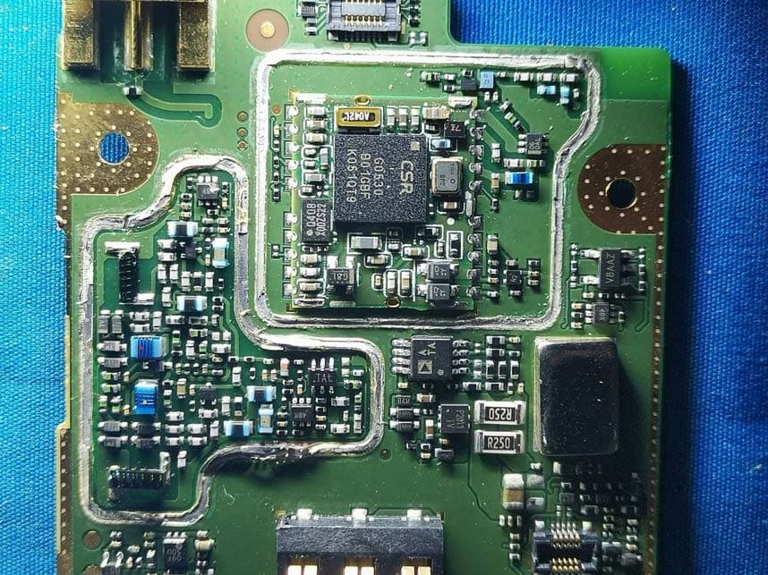
YAMHP6XXUMS
Jul 22, 2021Digital Portable Radio
Equipment Class
DTS - Digital Transmission System