YHI-VTC6110X00Intelligent Vehicle Telematics Computer
NEXCOM international Co.,LTD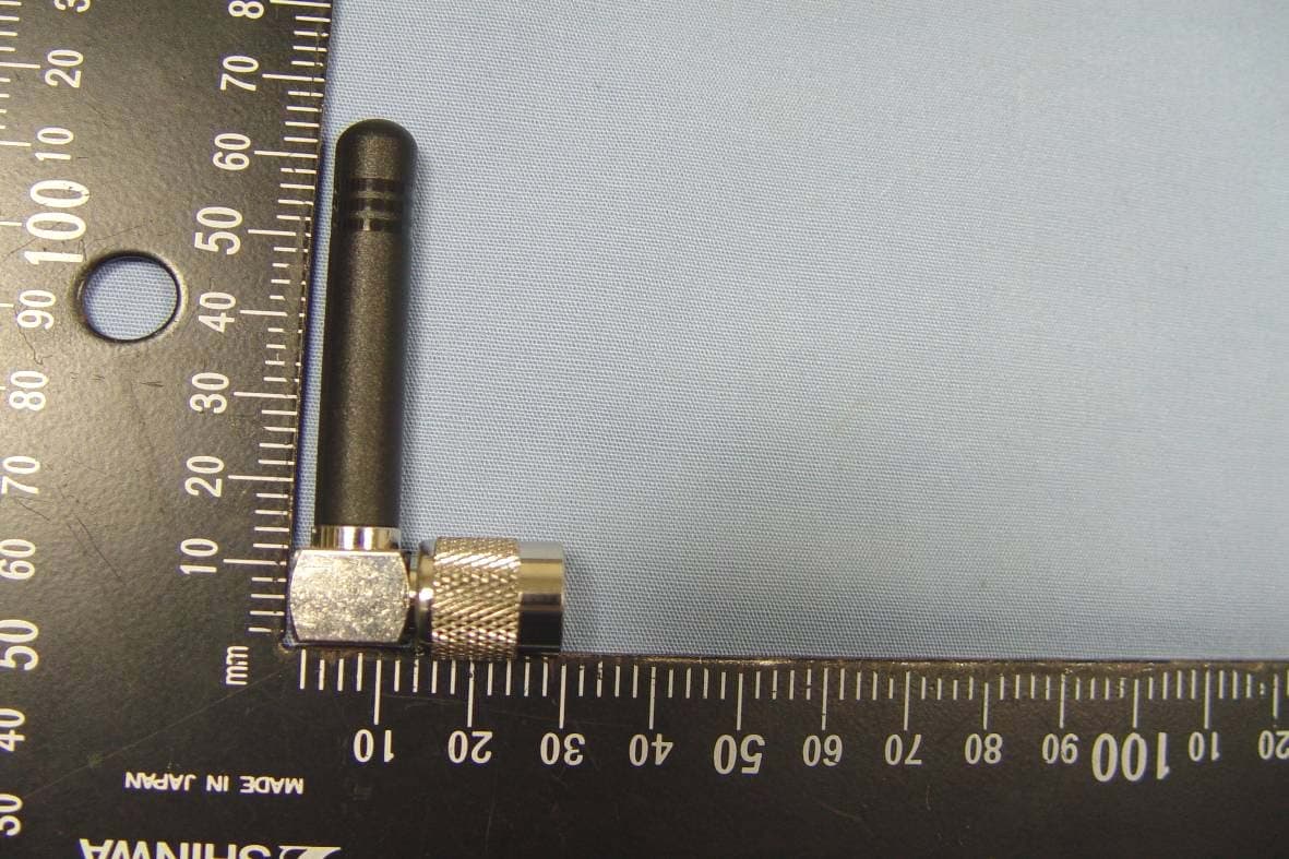
Click to zoom
Application Details
- Equipment Class
- PCB - PCS Licensed Transmitter
- Date of Grant
- Sep 29, 2010
- Application Purpose
- Original Equipment
- Date of Application
- Sep 29, 2010
- Equipment Note
- Intelligent Vehicle Telematics Computer
- Frequency Range
- 1852.40000000 - 1907.60000000
- Company
- NEXCOM international Co.,LTD
- Country
- Taiwan
Documents & Files
Document Text
Text extracted from the exhibit documents filed with the FCC. Open a document above to read the original.
Users Manual
NEXCOM International Co., Ltd. NEXCOM International Co., Ltd. Published January 2010 www.nexcom.com Mobile Computing Solutions Vehicle Telematics Computer VTC 6110 User Manual Copyright © 2009 NEXCOM International Co., Ltd. All Rights Reserved. ii VTC 6110 User Manual Contents Contents Preface Copyright .............................................................................................iv Disclaimer .............................................................................................iv Acknowledgements ..............................................................................iv Regulatory Compliance Statements .......................................................iv Declaration of Conformity ......................................................................iv RoHS Compliance ...................................................................................v Warranty and RMA ................................................................................vi Safety Information ................................................................................vii Installation Recommendations ................................................................vii Safety Precautions .................................................................................viii Technical Support and Assistance ...........................................................ix Conventions Used in this Manual ...........................................................ix Global Service Contact Information .........................................................x Package Contents ..................................................................................xii Ordering Information ............................................................................xiv Chapter 1: Product Introduction Overview ................................................................................................1 Key Features ...........................................................................................2 Hardware Specifications ..........................................................................2 COM Express CPU Module and Carrier Board ..........................................5 Physical Features .....................................................................................6 Front Panel ...........................................................................................6 Rear Panel ............................................................................................8 Mechanical Dimensions .........................................................................12 Chapter 2: Jumpers And Connectors Before You Begin ..................................................................................13 Precautions ...........................................................................................13 Jumper .................................................................................................14 Locations of the Jumpers and Connectors .............................................15 VTCB6110 ..........................................................................................15 Jumper Settings ....................................................................................16 SW5: Input Voltage Selection ..............................................................16 SW6: COM Port Mode Selection .........................................................16 CF (IDE0) Primary Master/Slave Select (JP4)..........................................16 LVDS Power Input Voltage Select (JP9) ................................................16 CMOS Input Voltage Select (J6)...........................................................16 BIOS Function Select (J1) .....................................................................16 DC Input Voltage Select (JP1) ..............................................................16 Temp Sensor (JP8) ...............................................................................17 Auto Power Select (JP2) ......................................................................17 PCI-104 VI/O Select Voltage (J13) ........................................................17 MCU Download (JP6) .........................................................................17 GAL Download (JP5) ...........................................................................17 MCU COM Port (JP3) ..........................................................................17 Connectors ...........................................................................................18 COM Express Row A and Row B .........................................................18 COM Express Row C and Row D .........................................................20 CompactFlash Connector....................................................................22 GPIO Connector .................................................................................23 RS232 Connector: COM1, COM2 .......................................................23 Copyright © 2009 NEXCOM International Co., Ltd. All Rights Reserved. iii Contents VTC 6110 User Manual RS232/485 Connector: COM3 ............................................................24 GAL Programmer PIN Header ..............................................................24 MCU Programmer Pin Header .............................................................25 VGA Connector ..................................................................................25 LVDS Connector + USB0 .....................................................................26 LAN Connector ...................................................................................27 USB Connector USB 1 .........................................................................27 USB Connector USB 2 .........................................................................28 LVDS Power Connector .................................................................…
Text truncated - open the document above for the full version.
Users Manual
Copyright © 2009 NEXCOM International Co., Ltd. All Rights Reserved. 7 VTC 6110 User Manual Chapter 1: Product Introduction LEDs GPIOI/O PORT Address : <Read/Write> #0EE0H Bit 0 : 0(Off) 1(On). COMMWLAN/HSDPA Status SIM Card Socket VTC 6110 can be internally integrated with a 3.5G Mini Card module. The SIM card bracket is on the carrier board. When using the GPRS/UMTS/HS- DPA function, insert the SIM card into the SIM card socket. Make sure to turn off VTC 6110 before inserting the SIM card. USB Port The USB port complies with USB 2.0 specifications. WiFi/Bluetooth Module Antenna Mounting Holes The 3 external antenna mounting holes are used to mount and connect WiFi antenna to a WLAN module (Mini Card type). GPRS/UMTS/HSDPA Module Antenna Mounting Hole The antenna mounting hole is used to mount and connect an antenna to the GPRS/UMTS/HSDPA module. Reset Button Press this button to restart VTC 6110. Line-out Line-out is a stereo output for connecting external speakers. Mic-in Mic-in receives monophonic input from an external microphone. Copyright © 2009 NEXCOM International Co., Ltd. All Rights Reserved. 8 VTC 6110 User Manual Chapter 1: Product Introduction Rear Panel ** Use power cable (+) with fuse for system protection Power Input DC Power Input Connector Connector location 3 2 1 Connector pin definition (CN1) Pin No.Function Description 1GND 2VIN(6V~36V) 3IGNITION VGA COM1 COM2 COM3 GPS LAN USB MIC-IN LINE-OUT DVI-D GPIO 5V/12V/SMBUS DC IN 6V-36V LVDS Copyright © 2009 NEXCOM International Co., Ltd. All Rights Reserved. 9 VTC 6110 User Manual Chapter 1: Product Introduction RS232/485 Connector COM3 The 9 pin D-Sub COM 3 port can be configured as RS232 or RS485 using the SW6 dip switch. Connector size: DSUB-9 PIN Connector location Connector pin definition PIn DefinitionPinDefinition 1DCD (RS232) TX-/RX- (RS485) 2RXD (RS232) TX+/RX+ (RS485) 3TXD (RS232)4DTR (RS232) 5GND6DSR (RS232 ) 7RTS (RS232)8CTS (RS232) 9RI (RS232) RS232 Connector COM1 and COM2 Connector size: DSUB-9 PIN Connector location Connector pin definition PIn DefinitionPinDefinition 1DCD 2RXD 3TXD4DTR 5GND6DSR 7RTS8CTS 9RI 1 5 6 9 1 5 6 9 Copyright © 2009 NEXCOM International Co., Ltd. All Rights Reserved. 10 VTC 6110 User Manual Chapter 1: Product Introduction LVDS Connector size: DB-26 PIN Connector location Connector pin definition PinDefinitionPinDefinition 1 Panel_ EN2 Panel_control 3 VDD4 VDD 5 LCDD09(OUT3)6 LCDD01(OUT0) 7 LCDD08(OUT3#)8 LCDD00(OUT0#) 9 LCDD_GND10 LCDD_GND 11 LCDD07(CLK)12 LCDD03(OUT1) 13 LCDD06(CLK#)14 LCDD02(OUT1#) 15 LVDS_GND16 LCDD_GND 17 LCDD05(OUT2)18 Power on push button 19 LCDD04(OUT2#)20 Panel_backlight 21 LCDD_GND22 Panel-Gnd 23 USB_0#24 Contact_DET# 25 USB_026 USB_VCC External SMBus, 12V and 5V Power Output Connector location 6 4 3 1 Connector pin definition PIn DefinitionPinDefinition 1 5V2 12V 3 SMBus Clock4 GND 5 GND6 SMBus Data +5 VDC (1A) and +12VDC (1A) power output and SMBus (w/o VTK 33M-01 connection) +5 VDC (0.5A) and +12VDC (0.5A) power output and SMBus (w/ VTK 33M-01 connection) Copyright © 2009 NEXCOM International Co., Ltd. All Rights Reserved. 11 VTC 6110 User Manual Chapter 1: Product Introduction VGA Port The DB15 VGA port supports resolutions up to 1600x1200 @ 85 Hz, 2048x1536 @ 60Hz. USB Port x 2 The two USB ports are compliant with USB 2.0 specifications. LAN Port The LAN port is an RJ45 interface with integrated LEDs and supports 10/100/1000Mbps Ethernet data transfer rates. Audio Jacks (MIC-IN and LINE-OUT) MIC-IN jack receives monophonic input from an external microphone. • LINE-OUT jack is the stereo output for connecting external speakers.• Copyright © 2009 NEXCOM International Co., Ltd. All Rights Reserved. 12 VTC 6110 User Manual Chapter 1: Product Introduction Mechanical Dimensions 260.0 50.0 176.0 Copyright © 2009 NEXCOM International Co., Ltd. All Rights Reserved. 13 Chapter 2: Jumpers and Connectors VTC 6110 User Manual Ch a p t e r 2: Ju m p e r s a n d Co n n eC t o r s This chapter describes how to set the jumpers on the motherboard. Note that the following procedures are generic for all VTC 6110 series. Before You Begin Ensure you have a stable, clean working environment. Dust and dirt can • get into components and cause a malfunction. Use containers to keep small components separated. Adequate lighting and proper tools can prevent you from accidentally • damaging the internal components. Most of the procedures that follow require only a few simple tools, including the following: A Philips screwdriver • A flat-tipped screwdriver • A set of jewelers Screwdrivers • A grounding strap • An anti-static pad • Using your fingers can disconnect most of the connections. It is recom-• mended that you do not use needle-nosed pliers to disconnect connec- tions as these can damage the soft metal or plastic parts of the connec- tors. Before working on internal components, make sure that the power • is off. Ground yourself before touching any internal components, by touching a metal object. Static electricity can damage many of the elec- tronic components. Humid environment tend to have less static electric- ity than dry environments. A grounding strap is warranted whenever danger of static electricity exists. Precautions Computer components and electronic circuit boards can be damaged by discharges of static electricity. Working on the computers that are still con- nected to a power supply can be extremely dangerous. Follow the guidelines below to avoid damage to your computer or your- self: Always disconnect the unit from the power outlet whenever you are • working inside the case. If possible, wear a grounded wrist strap when you are working inside • the computer case. Alternatively, discharge any static electricity by touching the bare metal chassis of the unit case, or the bare metal body of any other grounded appliance. Hold electronic circuit boards by the edges only. Do not touch the com-com-• ponents on the board unless it is necessary to do so. Don’t flex or st…
Text truncated - open the document above for the full version.
Users Manual
Copyright © 2009 NEXCOM International Co., Ltd. All Rights Reserved. 27 Chapter 2: Jumpers and Connectors VTC 6110 User Manual LAN Connector Connector size: RJ-45 Connector location: LAN1 Connector Pin Definition PinDefinitionPinDefinition 1 TX+2 TX- 3 RX+4 N/C1 5 N/C26 RX- 7 N/C38 N/C4 9 LAN Speed LED10 +3.3V 11 LAN Link LED12 +3.3V USB Connector Connector location: USB1 Connector Pin Definition PinDefinitionPinDefinition 1VCC2DATA- 3DATA+4GND Copyright © 2009 NEXCOM International Co., Ltd. All Rights Reserved. 28 Chapter 2: Jumpers and Connectors VTC 6110 User Manual Connector Pin Definition PinDefinitionPinDefinition 1 VCC2 DATA1- 3 DATA1+4 GND 5 VCC6 DATA- 7 DATA+8 GND USB Connector Connector location: USB2 LVDS Power Connector Connector location: J5 1 Connector Pin Definition PinDefinitionPinDefinition 1 Panel_backlight2 Panel_VDD 3 GND4 GND 5 LVDS_PANEL6 LVDS_BIASON Copyright © 2009 NEXCOM International Co., Ltd. All Rights Reserved. 29 Chapter 2: Jumpers and Connectors VTC 6110 User Manual External 12V & 5V Power and SMBUS Connector Connector location: CN2 6 3 4 1 Connector Pin Definition PinDefinitionPinDefinition 1 5V2 12V 3 SMBCLK4 GND 5 GND6 SMBDATA Mic-in Connector location: CN11 and CN15 Connector Pin Definition PinDefinitionPinDefinition 1 NC2 MIC_JD 3 NC4 MIC_OUT 5 GND6 GND Copyright © 2009 NEXCOM International Co., Ltd. All Rights Reserved. 30 Chapter 2: Jumpers and Connectors VTC 6110 User Manual Line-out Connector location: CN8 and CN14 Connector Pin Definition PinDefinitionPinDefinition 1 LINE_OUT_L2 SURR_JD 3 NC4 LINE_OUT_R 5 GND6 GND PCI-104 VI/O Voltage Setting Connector location: J13 Connector Pin Definition Pin No.StatusFunction Description 1-3, 2-4 (default)Short +3.3V 3-5, 4-6Short +5V 462 351 Copyright © 2009 NEXCOM International Co., Ltd. All Rights Reserved. 31 Chapter 2: Jumpers and Connectors VTC 6110 User Manual PCI-104 Connector Connector location: CN16 Connector Pin Definition Power Button Connector location: SW1 Reset Button Connector location: SW2 Copyright © 2009 NEXCOM International Co., Ltd. All Rights Reserved. 32 Chapter 2: Jumpers and Connectors VTC 6110 User Manual MCU COM Port Connector location: JP3 Connector Pin Definition PinFunction Description 1TX 2RX 3GND ACC_ON LED Connector location: JP7 1 Connector Pin Definition PinFunction Description 1 +3.3V LED 2 GND Copyright © 2009 NEXCOM International Co., Ltd. All Rights Reserved. 33 Chapter 2: Jumpers and Connectors VTC 6110 User Manual Temp Sensor Connector location: JP8 1 Connector Pin Definition PinFunction Description 1 SENSOR+ 2 GND DC Power Input Connector Connector location: CN1 Connector Pin Definition PinFunction Description 1 GND 2 VIN (6V~36V) 3 IGNITION Copyright © 2009 NEXCOM International Co., Ltd. All Rights Reserved. 34 Chapter 2: Jumpers and Connectors VTC 6110 User Manual Power On and IDE Active LED Connector location: LED1 T1 B1 Connector Pin Definition LEDFunction Description T1 POWER LED B1 HD LED GPIO and UMTS LEDs Connector location: LED2 T2 B2 LED I/O Port Address and Data LEDFunction Description T2 I/O PORT Address: 0EE0; Bit0: 1 (Light), 0 (Dark) B2 UMTS STATUS Copyright © 2009 NEXCOM International Co., Ltd. All Rights Reserved. 35 Chapter 2: Jumpers and Connectors VTC 6110 User Manual Serial ATA Connector location: CN6 17 Connector Pin Definition PinDefinitionPinDefinition 1 GND2 SATA_TXP0 - 3 SATA_TXN04 GND 5 SATA_RXN06 SATA_RXP0 7 GND Serial ATA Power Input Connector location: J10 1 4 Connector Pin Definition PinDefinitionPinDefinition 1+V12S2GND 3GND4+V5S Copyright © 2009 NEXCOM International Co., Ltd. All Rights Reserved. 36 Chapter 2: Jumpers and Connectors VTC 6110 User Manual Mini-PCIe Socket (for 3.5G module) PCIe Interface Connector location: CN10 1 2 51 52 Connector Pin Definition PinDefinitionPinDefinitionPinDefinitionPinDefinition 1MIC +2+V3.3S27GND28NC 3MIC -4GND29GND30NC 5SPK +6NC31NC32NC 7GND8USIM PWR33RESET34GND 9GND10USIM DATa35GND36USB_D- 11VCC_ MSM26_ DIG 12USIM CLK37GND38USB_D+ 13NC14USIM RST39+V3.3S40GND 15GND16NC41+V3.3S42LED_ WWAN# 17NC18GND43GND44NC 19NC20W_DIS- ABLE# 45NC46NC 21GND22NC47NC48NC 23NC24NC49NC50GND 25NC26GND51NC52+V3.3S Mini-PCIe Socket (for WLAN module) USB + PCIe Interface Connector location: CN13 1 2 51 52 Connector Pin Definition PinDefinitionPinDefinitionPinDefinitionPinDefinition 1WAKE#2+V3.3S27GND28+V1.5S 3NC4GND29GND30SMB_CLK 5NC6+V1.5S31PETn032SMB_DATA 7CLKREQ#8NC33PETp034GND 9GND10NC35GND36USB_D- 11REFCLK-12NC37NC38USB_D+ 13REFCLK+14NC39NC40GND 15GND16NC41NC42LED_ WWAN# 17NC18GND43NC44LED_ WLAN# 19NC20DISABLE#45NC46LED_ WPAN# 21GND22PERST#47NC48+V1.5S 23PERn024+3.3S49NC50GND 25PERp026GND51NC52+V3.3S Copyright © 2009 NEXCOM International Co., Ltd. All Rights Reserved. 37 Chapter 2: Jumpers and Connectors VTC 6110 User Manual SIM Card Connector Connector location: CN4 Connector Pin Definition PinDefinitionPinDefinition C1 POWER VOLTAGEC2 RESET SIGNAL C3 CLOCK SIGNALC5 GND C6 VPP:PROGRAM VOLTAGEC7 I/O SW Contact present switch Bluetooth Connector Connector location: J7 J7 JST-1mm-M-90 1 2 3 MH1 MH2 4 5 6 10 9 8 7 PinDefinitionPinDefinition 1 GND2 USB_6P_L 3 USB_6N_L4 NC 5 NC6 BT_AUDIO_EN_R 7 NC8 BT_3.3V 9 NC10 GND Copyright © 2009 NEXCOM International Co., Ltd. All Rights Reserved. 38 Chapter 3: System Setup VTC 6110 User Manual Ch a p t e r 3: Sy S t e m Se t u p Removing the Chassis Cover Front View 2. Lift the cover upward then remove it from the chassis. Bottom View Prior to removing the chassis cover, make sure the unit’s power is off and disconnected from the power sources to prevent electric shock or system damage. 1. The screws on the cover are used to secure the cover to the chassis. Remove these screws and put them in a safe place for later use. Rear View Copyright © 2009 NEXCOM International Co., Ltd. All Rights Reserved. 39 Chapter 3: System Setup VTC 6110 User Manual Installing a GPRS/UMTS/HSDPA Module 1. The Mini PCI Express slot shown below is used to install a 3.5G com- munication module such as GPRS, UMTS …
Text truncated - open the document above for the full version.
Users Manual
Copyright © 2009 NEXCOM International Co., Ltd. All Rights Reserved. 57 Chapter 3: System Setup VTC 6110 User Manual Installing the USB Cable Holder The USB cable holder is used to stabilize the USB cable so as to prevent it from getting loose when accidentally pulled or moved. 1. Attach the cable holder to the mounting hole by using the provided screw. 2. Hook the cable to the holder as shown in the photo below. Cable holder Copyright © 2009 NEXCOM International Co., Ltd. All Rights Reserved. 58 Chapter 3: System Setup VTC 6110 User Manual 2. Now mount the system on the wall by fastening screws through the bracket’s mounting holes. Fasten screws to mount the system to the wall Rackmount Brackets The rackmount brackets provide a convenient and economical way of mounting the system on the wall. 1. The mounting holes are located at the bottom of the system. Secure the brackets on each side of the system using the provided mounting screws. Rackmount bracket Secure the bracket to the system Copyright © 2009 NEXCOM International Co., Ltd. All Rights Reserved. 59 VTC 6110 User Manual Appendix A: I/O Address Function Ap p e n d i x A: i/O Ad d r e s s Fu n c t iO n GPIO LED / UMTS LED / Ignition Status I/O port : 0EE0H BitFunction Description Bit 0GPIO LED 0: OFF (default) 1: ON Bit 1UMTS LED 0: LED for WLAN (default) 1: LED for 3.5G and WLAN Bit 2Ignition (read only) 0: OFF 1: ON Bit 3Status of Vehicle Battery 0: Vehicle Battery is OK 1: Vehicle Battery is Low Voltage Bit0Bit1Bit2Bit3Bit4Bit5Bit6Bit7 Description8 bits data (Bit 7 is highest bit of data) Capacity of NEXCOM battery (8 bits) I/O port : 0EE1H Bit0Bit1Bit2Bit3Bit4Bit5Bit6Bit7 Description8 bits data (Bit 7 is highest bit of data) Voltage of NEXCOM battery (8 bits) I/O port : 0EE2H Copyright © 2009 NEXCOM International Co., Ltd. All Rights Reserved. 60 VTC 6110 User Manual Appendix A: I/O Address Function Status of NEXCOM battery (8 bits) I/O port : 0EE3H BitFunction Description Bit 0Status for G sensor detection 0: Normal 1: Abnormal (X-axis or Y-axis degree is about 90 or -90) Bit 1Power mode 0: 24V system 1: 12V system Bit 2Fan mode 0: Auto 1: Always on Bit 3Status of Smart battery 0: No discharging 1: Discharging Bit 4Status of Fan R 0: Well 1: Failed Bit 5Status of Fan R 0: Action 1: Inaction Bit 6Status of Fan L 0: Well 1: Failed Bit 7Status of Fan L 0: Action 1: Inaction GPIO I/O port : 0EE4H BitFunction Description Bit 0-3GPO 1-4 Bit 4-7GPI 1-4 Copyright © 2009 NEXCOM International Co., Ltd. All Rights Reserved. 61 VTC 6110 User Manual Appendix A: I/O Address Function Onboard Module Disable/Enable I/O port : 0EE6H BitFunction Description Bit 0 3.5G module 0: Disable 1: Enable (default) Bit 1 WLAN module 0: Disable 1: Enable (default) Bit 2 External +12V power 0: Disable 1: Enable (default) Bit 3 External +5V power 0: Disable 1: Enable (default) Bit 2, 1, 0: Time Setting Bit 2~0Time (sec) 0001 (default) 0012 0104 0118 10016 10132 11064 111128 WDT I/O port : 0EE5H BitFunction Description Bit 3 WDT Disable/Enable 0: Disable (default) 1: Enable Auto clear WDT timer when reading/writing I/O port 0EE5H. Copyright © 2009 NEXCOM International Co., Ltd. All Rights Reserved. 62 VTC 6110 User Manual Appendix B: ICES200-L24 COM Express CPU Module Ap p e n d i x B: iCeS200-L24 COM ex p r eS S CpU MOdU Le Overview ICES 200 is a Type 2 COM Express Module that features Intel ® 945GME and ICH7M chipset; switch supports Intel ® Core™ 2 Duo and Intel ® Core™ 2 Duo LV processors with 533/667 MHz FSB. One DDR2 memory socket supports up to 2GB. The ICES 200 is integrated with Intel ® Graphics Media Accelerator (GMA950) and expands via PCI Express Graphics x16 lanes to the carrier board. It also supports other display interfaces including LFP or Dual channel LVDS. The high performance ICES 200 COM Express Module supports 2 x SATA, 8 x USB 2.0 and 4 PCIe x1 Lanes through the carrier board. Key Features Intel• ® Socket M supports Core™ 2 Duo / Core™ 2 Duo LV Processor Family Intel• ® 945GME Chipset One DDR2 SO-DIMM socket supports un-buffered non-ECC DDR2 • 533/667 up to 2GB Supports 2 x Serial ATA for high speed drives, 8 x USB 2.0 for fast pe-• ripherals Type 2 COM Express Module supports up to 21 Express lanes, 32 bit PCI • interface, one IDE and Gigabit LAN Copyright © 2009 NEXCOM International Co., Ltd. All Rights Reserved. 63 VTC 6110 User Manual Appendix B: ICES200-L24 COM Express CPU Module Display Integrated with Intel• ® Graphics Media Accelerator (GMA950) or expand via PCI Express Graphics x16 lanes / Dual SDVO CRT resolution up to 2048 x 1536 @ 60Hz, 1600 x 1200 @ 85Hz • One PCI Express x16 Lane down to the carrier board• Supports LFP (Local Flat Panel) LVDS interface with resolution up to 1366 • x 768 Supports Single channel for 18 bit / Dual Channel for 18 bit• Audio HD audio interface• COM Express Connectors AB • - VGA / LVDS / 8 x USB 2.0 / HD Audio / 2 x SATA / LAN / GPIO / LPC bus / 1 x PCIe x4 / 1 x PCIe x1 / 5 x PCIe x1 / SMBus (I2C) / SPI BIOS CD • - PCIe x16 / IDE / PCI System Monitor Derived from HW monitor • Monitors 4 voltages, 2 temperatures and 1 fan speed • 4 voltages (For +3.3 V, +5 V, +12 V, Vcore)• 2 temperatures (CPU and one external Temperature Sensor)• Power Requirements + 12 V, + 5 VSB, + 3.3 V RTC• Specifications CPU Support Supports Intel• ® Socket M, Core™ 2 Duo Family Processors Supports 533/667MHz FSB CPU• Main Memory 1 x DDR2 SO-DIMM socket• Chipset Intel• ® 945GME ICH7M I/O Controller Hub• BIOS Award System BIOS • Plug & Play support• 8Mbit Flash ROM• Onboard LAN Realtek PCI Express GbE 8111C-GR• Supports PXE LAN boot function• Supports Wake on LAN• Copyright © 2009 NEXCOM International Co., Ltd. All Rights Reserved. 64 VTC 6110 User Manual Appendix B: ICES200-L24 COM Express CPU Module Dimensions COM Express Basic Module Type 2• 95mm x 125mm• Copyright © 2009 NEXCOM International Co., Ltd. All Rights Reserved. 65 VTC 6110 User Manual Appendix B: ICES200-L24 COM Express CPU Module Mechanical Dimensions Copyri…
Text truncated - open the document above for the full version.
Attestation Statements
RF_160, Issue 02 Declaration of Authorization We Name: Address: City:Taipei Country: Taiwan Declare that: Name Representative of agent: Mr. James Lee (1) Agent Company name: Compliance Certification Service Inc Address: No. 11, Wugong 6th., Wugu Township, Taipei Country 24891 City: Taipei Country: Taiwan is authorized to apply for Certification of the following product(s): Product description: Intelligent Vehicle Telematics Computer Type designation: VTC6110 Trademark: NEXCOM on our behalf. Date:Jun 15 2010. City:Taipei. Name:Mr. Jay Liu (2) Notes: (1): Required for FCC application (2): For FCC it must be the Grantee Code “owner” or the authorized agent.
Cover Letter(s)
RF_160, Issue 02 Declaration of Authorization We Name: Address: City:Taipei Country: Taiwan Declare that: Name Representative of agent: Mr. James Lee (1) Agent Company name: Compliance Certification Service Inc Address: No. 11, Wugong 6th., Wugu Township, Taipei Country 24891 City: Taipei Country: Taiwan is authorized to apply for Certification of the following product(s): Product description: Intelligent Vehicle Telematics Computer Type designation: VTC6110 Trademark: NEXCOM on our behalf. Date:Jun 15 2010. City:Taipei. Name:Mr. Jay Liu (2) Notes: (1): Required for FCC application (2): For FCC it must be the Grantee Code “owner” or the authorized agent.
External Photos
Compliance Certification Services Inc. Report No.: T100525004 Date of Issue: July 9, 2010 A1 - 1 Total Page: 25 Rev. 00 APPENDIX 1 - PHOTOGRAPHS OF EUT EXTERNAL PHOTOGRAPHS OF EUT Compliance Certification Services Inc. Report No.: T100525004 Date of Issue: July 9, 2010 A1 - 2 Rev. 00 Compliance Certification Services Inc. Report No.: T100525004 Date of Issue: July 9, 2010 A1 - 3 Rev. 00 Compliance Certification Services Inc. Report No.: T100525004 Date of Issue: July 9, 2010 A1 - 4 Rev. 00 Compliance Certification Services Inc. Report No.: T100525004 Date of Issue: July 9, 2010 A1 - 5 Rev. 00 Compliance Certification Services Inc. Report No.: T100525004 Date of Issue: July 9, 2010 A1 - 6 Rev. 00 WLAN & BT Antenna Compliance Certification Services Inc. Report No.: T100525004 Date of Issue: July 9, 2010 A1 - 7 Rev. 00 3G Antenna Compliance Certification Services Inc. Report No.: T100525004 Date of Issue: July 9, 2010 A1 - 8 Rev. 00 GPS Antenna
Internal Photos
Compliance Certification Services Inc. Report No.: T100525004 Date of Issue: July 9, 2010 A1 - 9 Rev. 00 INTERNAL PHOTOGRAPHS OF EUT Compliance Certification Services Inc. Report No.: T100525004 Date of Issue: July 9, 2010 A1 - 10 Rev. 00 Bluetooth Antenna connector WLAN Antenna connecto r 3G Antenna connector Bluetooth Module WLAN Module 3G Module Compliance Certification Services Inc. Report No.: T100525004 Date of Issue: July 9, 2010 A1 - 11 Rev. 00 Compliance Certification Services Inc. Report No.: T100525004 Date of Issue: July 9, 2010 A1 - 12 Rev. 00 Compliance Certification Services Inc. Report No.: T100525004 Date of Issue: July 9, 2010 A1 - 13 Rev. 00 Compliance Certification Services Inc. Report No.: T100525004 Date of Issue: July 9, 2010 A1 - 14 Rev. 00 Compliance Certification Services Inc. Report No.: T100525004 Date of Issue: July 9, 2010 A1 - 15 Rev. 00
Internal Photos
Compliance Certification Services Inc. Report No.: T100525004 Date of Issue: July 9, 2010 A1 - 16 Rev. 00 WLAN Module Compliance Certification Services Inc. Report No.: T100525004 Date of Issue: July 9, 2010 A1 - 17 Rev. 00 Compliance Certification Services Inc. Report No.: T100525004 Date of Issue: July 9, 2010 A1 - 18 Rev. 00 BT Module Compliance Certification Services Inc. Report No.: T100525004 Date of Issue: July 9, 2010 A1 - 19 Rev. 00 Compliance Certification Services Inc. Report No.: T100525004 Date of Issue: July 9, 2010 A1 - 20 Rev. 00 Compliance Certification Services Inc. Report No.: T100525004 Date of Issue: July 9, 2010 A1 - 21 Rev. 00 3G Module Compliance Certification Services Inc. Report No.: T100525004 Date of Issue: July 9, 2010 A1 - 22 Rev. 00 Compliance Certification Services Inc. Report No.: T100525004 Date of Issue: July 9, 2010 A1 - 23 Rev. 00 Compliance Certification Services Inc. Report No.: T100525004 Date of Issue: July 9, 2010 A1 - 24 Rev. 00 GPS Module Compliance Certification Services Inc. Report No.: T100525004 Date of Issue: July 9, 2010 A1 - 25 Rev. 00
RF Exposure Info
Compliance Certification Services Inc. Report No.: T100525004-RP3 FCC ID: YHI-VTC6110X00 Date of Issue: July 9, 2010 Page 172 Rev. 00 APPENDIX I RADIO FREQUENCY EXPOSURE LIMIT EUT Specification EUT Intelligent Vehicle Telematics Computer Frequency band (Operating) WLAN: 2.412GHz ~ 2.462GHz WLAN: 5.18GHz ~ 5.32GHz / 5.50GHz ~ 5.70GHz WLAN: 5.745GHz ~ 5.825GHz Others: GSM / GPRS / EDGE 850: 824 ~ 849 MHz Device category Portable (<20cm separation) Mobile (>20cm separation) Others Exposure classification Occupational/Controlled exposure (S = 5mW/cm 2 ) General Population/Uncontrolled exposure (S=1mW/cm 2 ) Antenna diversity Single antenna Multiple antennas Tx diversity Rx diversity Tx/Rx diversity Max. output power 32.00 dBm (1584.89mW) Antenna gain (Max) -0.97 dBi (Numeric gain: 0.79) Evaluation applied MPE Evaluation* SAR Evaluation N/A Remark: 1. The maximum output power is 32.00 dBm (1584.89mW) at 824.20MHz (with 0.79 numeric antenna gain.) 2. DTS device is not subject to routine RF evaluation; MPE estimate is used to justify the compliance. 3. For mobile or fixed location transmitters, no SAR consideration applied. The maximum power density is 1.0 mW/cm 2 even if the calculation indicates that the power density would be larger. TEST RESULTS No non-compliance noted. Compliance Certification Services Inc. Report No.: T100525004-RP3 FCC ID: YHI-VTC6110X00 Date of Issue: July 9, 2010 Page 173 Rev. 00 Calculation Given d GP E ×× = 30 & 3770 2 E S= Where E = Field strength in Volts / meter P = Power in Watts G = Numeric antenna gain d = Distance in meters S = Power density in milliwatts / square centimeter Combining equations and re-arranging the terms to express the distance as a function of the remaining variabl…
Text truncated - open the document above for the full version.
Contact Information
Applicant
Jay Liu(Assistant Vice President)
Technical Contact
Compliance Certification Services Inc.James Lee
[email protected]886 2 2299 9720
134, Wu Kung Rd, Wuku Industrial Zone · Taipei Hsien · Taiwan
Non-Technical Contact
Compliance Certification Services Inc.Natasha Tai
886 2 87525332
Test Firm
Compliance Certification Services Inc.Hank Lee
Technical Specifications
| # | Rule Parts | Frequency Range | Power Output | Emission | Tolerance |
|---|---|---|---|---|---|
| 8 | 24E | 1.85 GHz - 1.91 GHz | 289.10 mW | 4M16F9W | 45 Hz |
Other Applications from NEXCOM international Co.,LTD
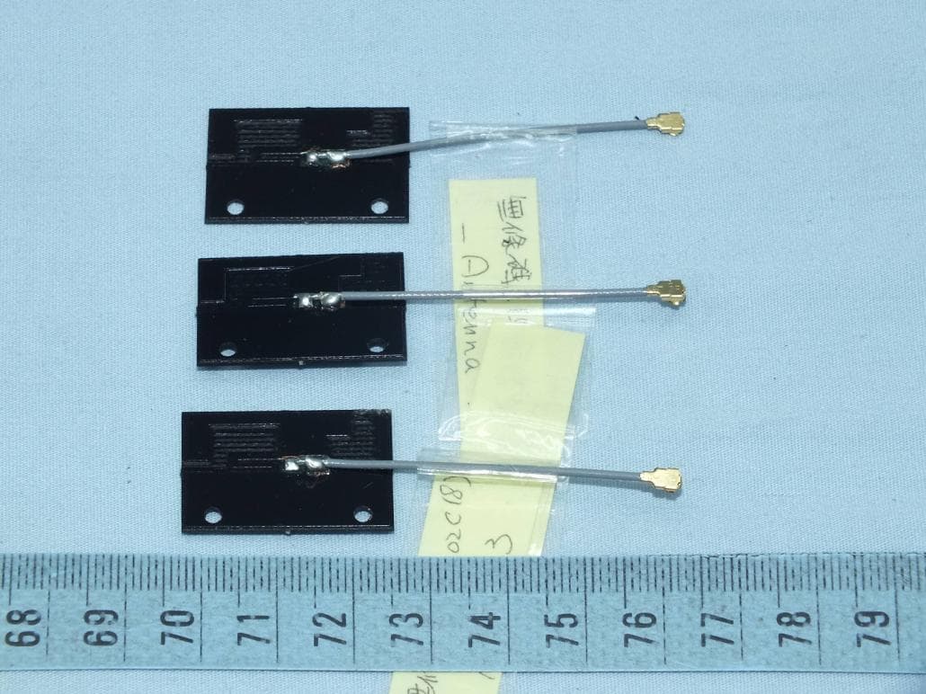
YHI-NW111
Jan 03, 20163x3 11n/g/b/a 2.4/5GHz WiFi Module
Equipment Class
DTS - Digital Transmission System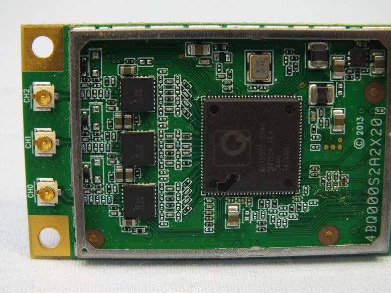
YHI-NW121
Dec 30, 20153x3 11ac/n/g/b/a 2.4/5GHz WiFi Module
Equipment Class
DTS - Digital Transmission System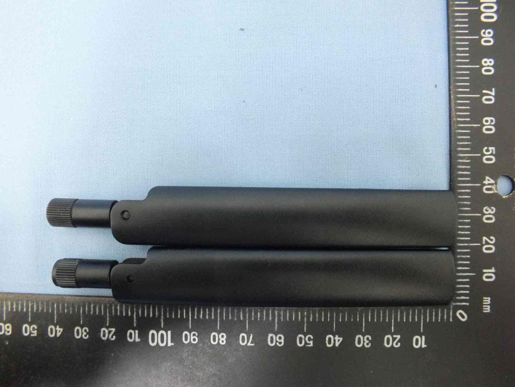
YHI-EWF3210K
Apr 29, 2015Industrial IEEE 802.11a/b/g/n AP module
Equipment Class
DTS - Digital Transmission System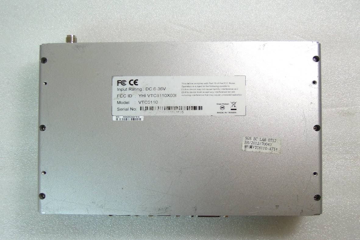
YHI-VTC6110ATT4
Sep 09, 2012VTC6110-ATT4
Equipment Class
PCB - PCS Licensed Transmitter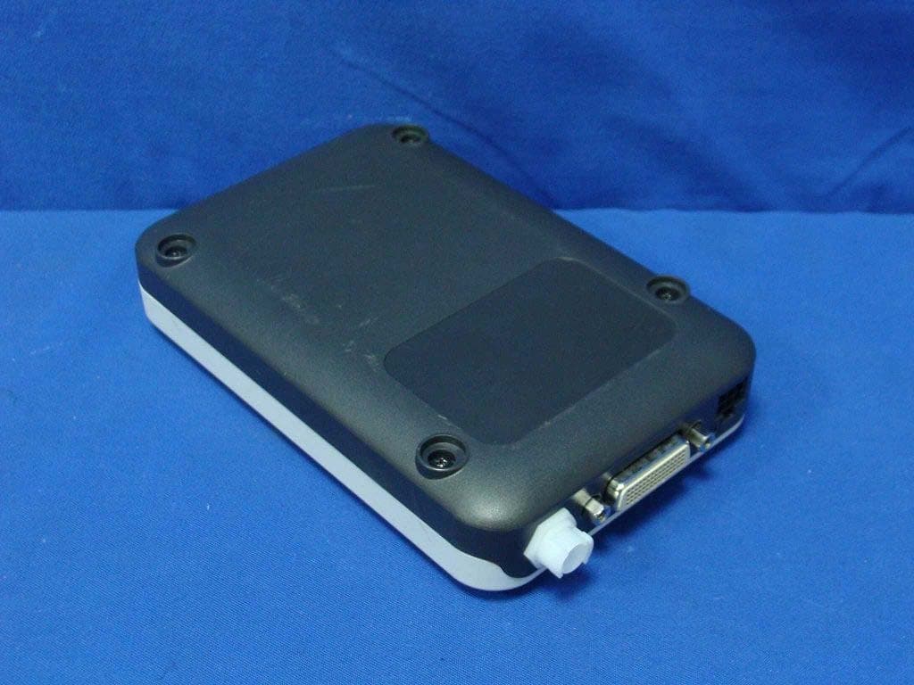
YHI-V10001
Dec 07, 2011Link Box
Equipment Class
DTS - Digital Transmission System