Z64-CC3100KITAEvaluation board
Texas Instruments Incorporated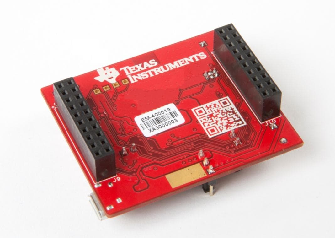
Click to zoom
Application Details
- Equipment Class
- DTS - Digital Transmission System
- Date of Grant
- May 06, 2014
- Application Purpose
- Original Equipment
- Date of Application
- May 05, 2014
- Equipment Note
- Evaluation board
- Frequency Range
- 2412.00000000 - 2462.00000000
- Country
- United States
Documents & Files
Document Text
Text extracted from the exhibit documents filed with the FCC. Open a document above to read the original.
Users Manual
User Guide 2014 SimpleLink is a trademark of Texas Instruments Incorporated. TI Proprietary Information - Strictly Private 1 CC3100BOOST (CC3100 Booster Pack) User Guide, Ver 1.1 ECS Applications ABSTRACT This document describes the CC3100BOOST (CC3100 Booster Pack). It details the features of the hardware and also explains the correct usage of the board. ABSTRACT This document describes the CC3100BOOST (CC3100 Booster Pack). It details the features of the hardware and also explains the correct usage of the board. The antenna(s) used for this transmitter must be installed to provide a separation distance of at least 20 cm from all persons and must not be co-located or operating in conjunction with any other antenna or transmitter CC3100BOOST User Guide TI Proprietary Information - Strictly Private TABLE OF CONTENTS 1 Introduction ................................................................................................................................ 4 2 Overview ...................................................................................................................................... 4 3 Hardware description ................................................................................................................ 4 3.1 Board overview ....................................................................................................................... 4 3.2 Board features ........................................................................................................................ 5 3.3 Jumper and connector information ......................................................................................... 6 3.3.1 2x20 pin connector ...................................................................................................... 6 3.4 Jumper details ........................................................................................................................ 7 3.5 LED and switches .................................................................................................................... 8 3.6 Conducted testing ................................................................................................................... 9 3.7 Current measurement ........................................................................................................... 10 4 Connecting to a PC using FTDI Board ................................................................................... 11 4.1 Jumper settings on the BP Board .......................................................................................... 11 4.2 Jumper settings on the FTDI Board ...................................................................................... 12 4.3 FTDI Board details ................................................................................................................ 13 4.3.1 Overview ................................................................................................................... 13 4.3.2 Hardware details ....................................................................................................... 14 4.3.3 Driver requirements .................................................................................................. 15 5 Connecting to a Launchpad .................................................................................................... 16 5.1 Launchpad current limitation ................................................................................................ 16 5.2 Connecting to an experimenter’s board. ............................................................................... 18 CC3100BOOST User Guide TI Proprietary Information - Strictly Private CC3100BOOST User Guide TI Proprietary Information - Strictly Private 1 Introduction This document provides a quick start guide on using the CC3100 Booster Pack Rev 2.0B . This is not applicable to other revisions of the board. 2 Overview The CC3100 Booster Pack is a board designed to interface with the TI standard Launchpad including the Tiva-C series and the MSP430 value line launchpads. In addition to the launchpads, there is support available to mate the board with a FTDI Debug board to interface directly to a PC host using USB cable. A picture of the board is presented below with the main components marked. 3 Hardware description 3.1 Board overview CC3100BOOST User Guide TI Proprietary Information - Strictly Private FIGURE 1 : HARDWARE DETAILS 3.2 Board features 2x20 pin stackable connectors On-board chip antenna with option for U.FL based conducted testing. Power from on-board LDO using USB OR 3.3V from MCU Launchpad Push buttons (2x) LEDs (4x) Jumper with 0.1 Ohm resistor for current measurement. .8 Mbit serial flash 40 MHz crystal , 32KHz crystal and oscillator. CC3100 RESET Current Measurement RESET BUTTON Sense on Power GPIO13 U.FL Antenna RF SIGNAL SELECT TOP DIE FLASH Vcc CC3100 Vcc GPIO12 USB CONN SERIAL FLASH CC3100BOOST User Guide TI Proprietary Information - Strictly Private 4 Layer PCB with 6mil spacing and track width. 3.3 Jumper and connector information 3.3.1 2x20 pin connector The signal assignment on the 2x20 pin connector is shown below. The convention of J1..J4 is replaced with P1...P4 to avoid confusion with the actual board reference. Outer row connectors Pin No Signal Name Direction Pin No Signal Name Direction P1.1 VCC(3.3V) IN P2.1 GND IN P1.2 UN-USED NA P2.2 IRQ OUT P1.3 UART1_TX OUT P2.3 SPI_CS IN P1.4 UART1_RX IN P2.4 UN-USED NA P1.5 nHIB IN P2.5 nRESET IN P1.6 UNUSED NA P2.6 SPI_MOSI IN P1.7 SPI_CLK IN P2.7 SPI_MISO OUT P1.8 UN-USED NA P2.8 UN-USED NA P1.9 UN-USED NA P2.9 UN-USED NA P1.10 UN-USED NA P2.10 UN-USED NA Inner row connectors Pin No Signal Name Direction Pin No Signal Name Direction P3.1 +5V IN P4.1 ANT_SEL_1 OUT P3.2 GND IN P4.2 ANT_SEL_2 OUT P3.3 UN-USED NA P4.3 UN-USED NA P3.4 UN-USED NA P4.4 UART1_CTS IN P3.5 UN-USED NA P4.5 UART1_RTS OUT P3.6 UN-USED NA P4.6 UN-…
Text truncated - open the document above for the full version.
External Photos
CC3100BOOSTA External Photos: Top Side: Bottom Side: Texas Instruments Incorporated
ID Label/Location Info
CC3100BOOSTA FCC ID/IC labeling: The product ID’s are printed in silk on the circuit board as shown below. Bottom side of circuit board: Texas Instruments Incorporated
Internal Photos
CC3100BOOSTA External Photos: Top Side: Bottom Side: Texas Instruments Incorporated
Operational Description
CC3100BOOSTA Operating Description: The CC3100BOOSTA is an evaluation board for the CC3100 device from Texas Instruments. The CC3100 device is an 802.11bgn Wi-Fi network processor designed for embedded applications that use low cost and low performance microcontrollers. The CC3100BOOSTA evaluation board will only function when attached to a Texas Instrument’s Tiva-C series or MSP430 value line microcontroller launchpad evaluation board or when attached to a Texas Instrument’s CC31xxEMUBOOST FTDI debug board. The Texas Instrument’s CC31xxEMUBOOST FTDI debug board allows the CC3100BOOSTA to interface directly to a PC host using USB cable. In this configuration the PC emulates the low cost microcontroller. The CC3100BOOSTA evaluation board comes with a software development kit that allows the user to execute demonstration code to evaluate the Wi-Fi function and features of the CC3100 device. The user can also execute code that they have developed. The code will execute on a Texas Instrument microcontroller. The microcontroller communicates with the CC3100BOOSTA evaluation board through a serial interface. The microcontroller can issue high level commands and associated data to the CC3100BOOSTA evaluation board through the serial interface. The CC3100BOOSTA evaluation board will then translate the commands and data into the associated 802.11 bgn Wi-Fi protocol and transmit them using the on board antenna or through an optional cable connector for conductive testing. The on board antenna is an integral chip antenna with nominal directional gain of 1.9 dBi. Texas Instruments Incorporated
RF Exposure Info
Prediction of MPE limit at a given distance Equation from page 18 of OET Bulletin 65, Edition 97-01 where:S = power density P = power input to the antenna G = power gain of the antenna in the direction of interest relative to an isotropic radiator R = distance to the center of radiation of the antenna Maximum peak output power at device output terminal:14.21dBm Cable and Jumper loss:0.0dB Maximum peak output power at antenna input terminal:14.21dBm 26.36331386mW Single Antenna gain (typical):1.9dBi Number of Antennae:1 Total Antenna gain (typical):1.9dBi 1.548816619(numeric) Prediction distance:20cm Prediction frequency:2437MHz MPE limit for uncontrolled exposure at prediction frequency:1mW/cm 2 Power density at prediction frequency:0.008123 mW/cm 2 0.081233W/m 2 Tx On time:1.000000ms Tx period time:1.000000ms Average Factor:100.000000% Average Power density at prediction frequency:0.081233W/m 2 Maximum allowable antenna gain:22.80269855dBi Margin of Compliance:20.90269855 dB 2 4R PG S π =
Test Report
www.nemko.com Nemko Canada Inc., a testing laboratory, is accredited by the Standards Council of Canada. The tests included in this report are within the scope of this accreditation FCC 15.247 and RSS-210 A8.docx; Date: May 2013 SCC Accredited LAB LAB Accrédité CCN TM ONE WORLDOURAPPROVAL Test report 257108-1TRFWL Date of issue: May 1, 2014 Applicant: Texas Instruments Inc. Product: CC3100 BoosterPack Model: CC3100BOOSTA FCC ID: IC Registration number: Z64-CC3100KITA 451I-CC3100KITA Specifications: FCC 47 CFR Part 15 Subpart C, §15.247 Operation in the 902–928 MHz, 2400–2483.5 MHz, 5725–5850 MHz RSS-210, Issue 8, December 2010, Annex 8 Frequency Hopping and Digital Modulation Systems Operating in the 902–928 MHz, 2400–2483.5 MHz, and 5725–5850 MHz Bands Report reference ID: 257108-1TRFWL Page 2 of 41 Test location Company name: Nemko Canada Inc. Address: 303 River Road City: Ottawa Province: Ontario Postal code: K1V 1H2 Country: Canada Telephone: +1 613 737 9680 Facsimile: +1 613 737 9691 Toll free: +1 800 563 6336 Website: www.nemko.com Site number: FCC: 176392; IC: 2040A-4 (3 m semi anechoic chamber) Tested by: Andrey Adelberg, Senior Wireless/EMC Specialist Reviewed by: Kevin Rose, Wireless/EMC Specialist Date: May 1, 2014 Signature: Limits of responsibility Note that the results contained in this report relate only to the items tested and were obtained in the period between the date of initial receipt of samples and the date of issue of the report. This test report has been completed in accordance with the requirements of ISO/IEC 17025. All results contain in this report are within Nemko Canada’s ISO/IEC 17025 accreditation. Copyright notification Nemko Canada Inc. authorizes the applicant to reproduce this report provided it is reproduced in its entirety and for use by the company’s employees only. Any use which a third party makes of this report, or any reliance on or decisions to be made based on it, are the responsibility of such third parties. Nemko Canada Inc. accepts no responsibility for damages, if any, suffered by any third party as a result of decisions made or actions based on this report. © Nemko Canada Inc. Report reference ID: 257108-1TRFWL Page 3 of 41 Table of contents Table of contents .......................................................................................................................................................................................................... 3 Section 1. Report summary ................................................................................................................................................................................. 4 1.1 Applicant and manufacturer .................................................................................................................................................................................... 4 1.2 Test specifications .................................................................................................................................................................................................... 4 1.3 Test methods ............................................................................................................................................................................................................ 4 1.4 Statement of compliance ......................................................................................................................................................................................... 4 1.5 Exclusions ................................................................................................................................................................................................................. 4 1.6 Test report revision history ...................................................................................................................................................................................... 4 Section 2. Summary of test results ....................................................................................................................................................................... 5 2.1 FCC Part 15 Subpart C, general requirements test results ........................................................................................................................................ 5 2.2 FCC Part 15 Subpart C, intentional radiators test results.......................................................................................................................................... 5 2.3 IC RSS-GEN, Issue 3, test results ............................................................................................................................................................................... 5 2.4 IC RSS-210, Issue 8, test results ................................................................................................................................................................................ 6 Section 3. Equipment under test (EUT) details ..................................................................................................................................................... 7 3.1 Sample information .................................................................................................................................................................................................. 7 3.2 EUT information ....................................................................................................................................................................................................... 7 3.3 Technical information .............................................................................................................................................................................................. 7 3.4 Product description and theory of operation .....................................................................…
Text truncated - open the document above for the full version.
Contact Information
Applicant
Marian Kost(Product Line Manager, Connectivity)
Test Firm
Nemko Canada Inc. (Ottawa)Charles Neal
Technical Specifications
| # | Rule Parts | Frequency Range | Power Output |
|---|---|---|---|
| 1 | 15C | 2.41 GHz - 2.46 GHz | 26.40 mW |
Other Applications from Texas Instruments Incorporated
Z64-CC33SBMOD
Jul 17, 2025802.11 b/g/n/ax WLAN + BLE Radio Module
Equipment Class
DTS - Digital Transmission System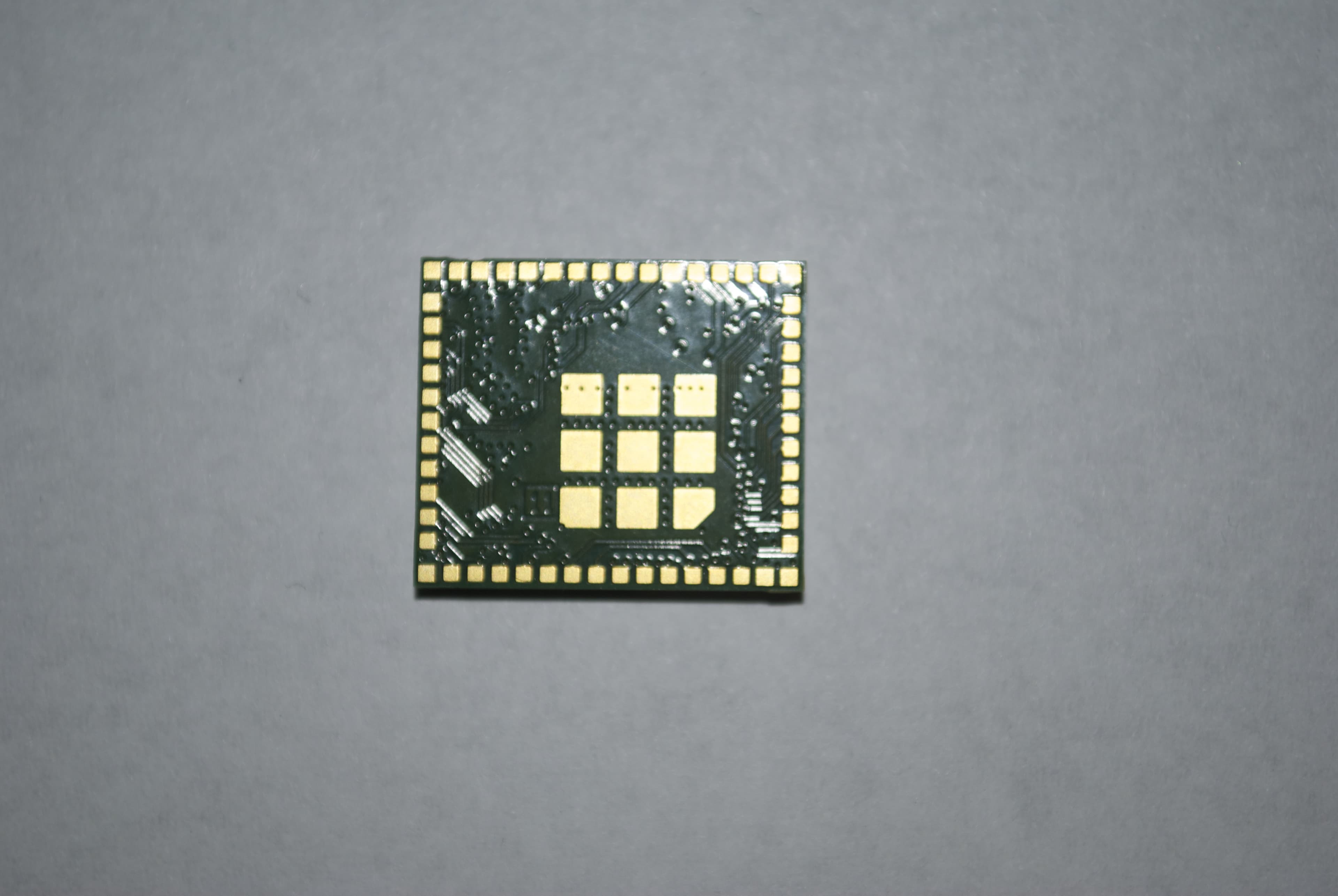
Z64-CC3200MODR1
Oct 08, 2014Radio Module
Equipment Class
DTS - Digital Transmission System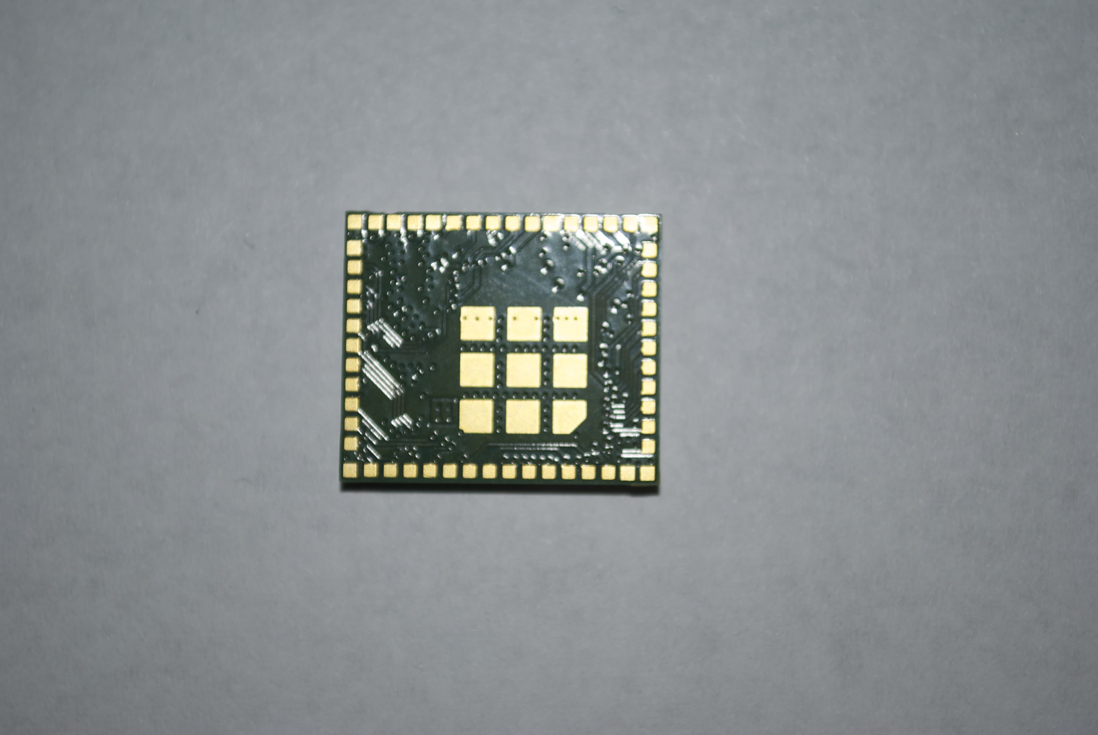
Z64-CC3100MODR1
Oct 08, 2014Radio Module
Equipment Class
DTS - Digital Transmission System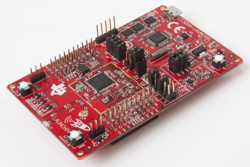
Z64-CC3200KITA
May 06, 2014Evaluation board
Equipment Class
DTS - Digital Transmission System
Z64-2564N
Mar 31, 2014CC2564 Bluetooth HCI Module
Equipment Class
DTS - Digital Transmission System