ZAT7IDEMThe 7IDEM is a development tool for TIs 2.4 GHz 7ID System-on-Chip
Texas Instruments Inc.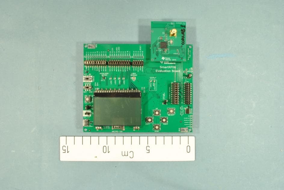
Click to zoom
Application Details
- Equipment Class
- DTS - Digital Transmission System
- Date of Grant
- Feb 27, 2014
- Application Purpose
- Original Equipment
- Date of Application
- Feb 24, 2014
- Equipment Note
- The 7IDEM is a development tool for TIs 2.4 GHz 7ID System-on-Chip
- Frequency Range
- 2402.00000000 - 2480.00000000
- Company
- Texas Instruments Inc.
- Country
- United States
Documents & Files
Document Text
Text extracted from the exhibit documents filed with the FCC. Open a document above to read the original.
Users Manual
TI Confidential – NDA Restrictions Page 1 of 4 CC2650 Packet Error Rate Test Quick Start Guide Version Updated 0.0.2 17. September 2013 Revised for rev 0.1.0 of PER Test CC2650 Packet Error Rate Test Quick Start Guide TI Confidential – NDA Restrictions Page 2 of 4 Functional Overview This guide describes how to use the Packet Error Rate (PER) test with CC2650. Prerequisites In order to use the PER test, please set up your SmartRF06EB according to the “CC2650 Alpha Release Quick start guide” as the silicon qual package can become damaged if not. Uploading firmware Upload the per_test.hex file to a CC2650 using the SmartRF Flash Programmer. Be sure to do full erase/program/verify of uploaded code. After upload, do a power cycling or pin reset to boot the PER test. Menu system The menu system is based on using the buttons on SmartRF06EB to navigate. There are 5 buttons needed LEFT – go back to previous menu UP/DOWN – navigate between menu elements RIGHT/SELECT – choose menu element Start menu The start menu contains the devices supported on the PER test, as well as a settings menu. Settings menu To see the difference in power consumption with and without the DC/DC converter, you can press RIGHT/SELECT on DCDC to toggle it on or off. A “1” indicates that it is currently on. Channel menu After selecting a device (e.g. CC2650EM), you can currently select the Bluetooth LE channel you would like to use for the test. Since the PER test is implemented using BLE Advertising packages (Non-connectable undirected advertising), only the advertising channels are available. Together, they cover the allowed frequency band for Bluetooth LE. 37 – 2402MHz 38 – 2426MHz 39 – 2480MHz CC2650 Packet Error Rate Test Quick Start Guide TI Confidential – NDA Restrictions Page 3 of 4 Mode menu In the mode menu, you can select which device is transmitting and which is receiving: BLE Transmitter BLE Receiver After selecting “BLE Receiver”, the device goes directly into receive mode and is ready to receive packets. Only let 1 PER test device with the advertising address 0x264026402640 transmit packages at the same time, as the receiver are based on recognizing a sequence number in the payload and will get restart the receive statistics if packets with a lower sequence number arrives. TX Power When selecting “BLE Transmitter”, you can also select which output power you would like to transmit with. Currently, the following options are available: 0 dBm +5dBm Burst size After selecting output power, you can also select the number of packets you would like to send in one test. This is configurable between 1000 and 1 000 000 packets. Packet rate To test the device with different data rates, you can also select how many packets per second you would like to send. This configures the 32k RTC timer to trigger an interrupt a number of times per second to send a package. Note: The PER test packet rate setting is currently using a low frequency clock derived from the 48MHz clock, meaning the packet rate is not 100% accurate. The RTC frequency is therefore 31.25kHz instead of 32.768 kHz but this will be changed in a later release. TX Idle The PER test is now ready to send packages but has not yet started. To start sending packages, press RIGHT/SELECT. You can restart the test at any time by pressing RIGHT or SELECT. CC2650 Packet Error Rate Test Quick Start Guide TI Confidential – NDA Restrictions Page 4 of 4 Current measurement To measure power consumption during test modes, connect a measurement device instead of the jumper ”VDD TO EM” on the SmartRF06EB. This can be e.g. a digital multi meter with the range set to mA or an oscilloscope. To get the lowest possible current consumption, restart the SmartRF06EB after programming the device and remove all the jumpers on the "JTAG Bypass" header (to avoid leakage current to the debugger on the SmartRF06EB). Also remove the tiny current measurement circuit next to the jumper, as the instrumentation amplifier will consume several microamperes. Note: If using an oscilloscope, do not use more than 1 ohm in series and make sure to run the board on 2xAAA batteries and move the board switch to BAT instead of USB. The scope ground will force the supply to each potential, shorting the on-board LDO on the SmartRF06EB. Known bugs and issues Regulatory Information The CC2650 evaluation module (7IDEM) is FCC and IC certified and tested to comply with ETSI R&TTE regulations over temperature from 0 to +35°C. The evaluation module has an integrated PCB antenna. FCC/IC Regulatory Compliance FCC Part 15 Class A Compliant IC ICES-003 Class A Compliant EVALUATIONBOARD/KIT/MODULE(EVM)ADDITIONALTERMS TexasInstruments(TI)providestheenclosedEvaluationBoard/Kit/Module(EVM)underthefollowingconditions: Theuserassumesallresponsibilityandliabilityforproperandsafehandlingofthegoods.Further,theuserindemnifiesTIfromallclaims arisingfromthehandlingoruseofthegoods. Shouldthisevaluationboard/kitnotmeetthespecificationsindicatedin theUser’s Guide,theboard/kitmaybereturnedwithin30daysfrom thedateofdeliveryfora fullrefund.THEFOREGOINGLIMITEDWARRANTYISTHEEXCLUSIVEWARRANTYMADEBYSELLERTO BUYERANDISINLIEUOFALLOTHERWARRANTIES,EXPRESSED,IMPLIED,ORSTATUTORY,INCLUDINGANYWARRANTYOF MERCHANTABILITYORFITNESSFORANYPARTICULARPURPOSE.EXCEPTTOTHEEXTENTOFTHEINDEMNITYSETFORTH ABOVE,NEITHERPARTYSHALLBELIABLETOTHEOTHERFORANYINDIRECT,SPECIAL,INCIDENTAL,ORCONSEQUENTIAL DAMAGES. PleasereadtheUser's Guideand,specifically,theWarningsandRestrictionsnoticein theUser's Guidepriortohandlingtheproduct.This noticecontainsimportantsafetyinformationabouttemperaturesandvoltages.ForadditionalinformationonTI's environmentaland/orsafety programs,pleasevisitwww.ti.com/eshorcontactTI. Nolicenseis grantedunderanypatentrightorotherintellectualpropertyrightofTIcoveringorrelatingtoanymachine,process,or combinationin whichsuchTIproductsorservicesmightbeorareused.TIcurrentlydealswitha varietyofcustomersforproducts,and thereforeourarrangementwiththe…
Text truncated - open the document above for the full version.
Block Diagram
7IDEM CC2650 f = <2400 MHz – 2480 MHz> LNA PA AAF ADCADC DEMODULATOR MODULATOR RADIO CONTROLLER AND DATA INTERFACE Q I RF_N RF_P I Q CLOCK MUX XOSC_Q2 XOSC_Q1 48 MHz RC-OSC 32 kHz RC-OSC 24 MHz Crystal OSC 32.768 kHz Crystal OSC BALUN ADC CLOCK RF PLL f_internal = <4800 MHz – 4960 MHz> f_output = <2400 MHz – 2480 MHz> CTRL X32K_Q2 X32K_Q1
External Photos
INTERNAL PHOTOS Projectno.:250971 FCC ID:ZAT7IDEM Page1(2) INTERNALPHOTOS–7IDEM 7IDEM–PCB component side 7IDEM–rear side INTERNAL PHOTOS Projectno.:250971 FCC ID:ZAT7IDEM Page2(2) 7IDEMwith evaluation board SmartRF06EB evaluation board SmartRF06EB-rear side with 2xAAAbatteries
ID Label/Location Info
Texas Instruments Norway AS Gaustadalléen 21 0349 Oslo Norway (+47) 23 36 98 11 (+47) 23 36 98 01 Description of FCC/IC/CE marking on 7IDEM The FCC/IC/CE labeling of the 7IDEM evaluation board is shown below. The label that indicates the assembly model name, FCC and IC identifiers are located on the back side of the board. ~ 41 mm ~ 4 7 m m Model: 7IDEM (xx) Rev. x.x.x S.No.: xxxxxx FCC ID: ZAT7IDEM IC: 451H-7IDEM Front side view Back side view
Internal Photos
INTERNAL PHOTOS Projectno.:250971 FCC ID:ZAT7IDEM Page1(2) INTERNALPHOTOS–7IDEM 7IDEM–PCB component side 7IDEM–rear side INTERNAL PHOTOS Projectno.:250971 FCC ID:ZAT7IDEM Page2(2) 7IDEMwith evaluation board SmartRF06EB evaluation board SmartRF06EB-rear side with 2xAAAbatteries
Operational Description
Texas Instruments Norway AS Gaustadalléen 21 0349 Oslo Norway (+47) 23 36 98 11 (+47) 23 36 98 01 Page 1 of 1 Technical Description The 7IDEM is an evaluation board for the CC2650 RF SoC from Texas Instruments. The 7IDEM is included in a development kit that can be used for Bluetooth Smart development. The 7IDEM is an engineering development board and cannot be used in an end product. The CC2650 System on Chip has a differential RF output. On the 7IDEM board this differential output is transformed to a single ended, 50 ohm signal through a passive component (capacitor/inductor) balun. The output of the balun is low pass filtered to reduce harmonic radiation and then connected to a PCB antenna.
Parts List/Tune Up Info
Part ReferenceQuantityValuePCB PackageDescriptionMPNManufacturer C212.2uF0402CAPACITOR, CERAMIC X5R, 2.2uF, 6.3V, -10%/+10%, -55DEGC/+85DEGC, 0402, SMDGRM155R60J225KE95DMURATA C3 C4 C5 C9 C10 C206100nF0402CAPACITOR, CERAMIC X7R, 100nF, 6.3V, -10%/+10%, -55DEGC/+125DEGC, 0402, SMDGRM155R70J104KA01DMURATA C6 C824.7uF0603CAPACITOR, CERAMIC X5R, 4.7uF, 6.3V, -10%/+10%, -55DEGC/+85DEGC, 0603, SMDGRM188R60J475KE19DMURATA C71100nF0603CAPACITOR, CERAMIC X7R, 100nF, 25V, -10%/+10%, -55DEGC/+125DEGC, 0603, SMDGRM188R71E104KA01DMURATA C11 C2121pF0402CAPACITOR, CERAMIC C0G/NP0, 1pF, 50V, -0.25pF/ +0.25pF, -55DEGC/+125DEGC, 0402, SMDGRM1555C1H1R0CA01DMURATA C12 C1321.2pF0402CAPACITOR, CERAMIC C0G/NP0, 1.2pF, 50V, -0.1pF/ +0.1pF, -55DEGC/+125DEGC, 0402, SMDGRM1555C1H1R2BA01DMURATA C14 C16212pF0402CAPACITOR, CERAMIC C0G/NP0, 12pF, 50V, -5%/+5%, -55DEGC/+125DEGC, 0402, SMDGRM1555C1H120JA01DMURATA C15 C22 C233DNM0402CAPACITOR, CERAMIC, N/A VALUE, -55DEGC/+125DEGC, 0402, SMDCAPACITOR_0402_DNM_N/A_MManufacturer selection C17 C18212pF0402CAPACITOR, CERAMIC C0G/NP0, 12pF, 50V, -5%/+5%, -55DEGC/+125DEGC, 0402, SMDCAPACITOR_0402_12pF_C0G/NP0_M_+/-5%_50VMANUFACTURER SELECTION C1911uF0402CAPACITOR, CERAMIC X5R, 1uF, 10V, -10%/+10%, -55DEGC/+85DEGC, 0402, SMDGRM155R61A105KE15DMURATA C3116.8pF0402CAPACITOR, CERAMIC C0G/NP0, 6.8pF, 50V, -0.25pF, +0.25pF, -55DEGC/+125DEGC, 0402, SMDGRM1555C1H6R8CA01DMURATA FL11BLM18HE152SN10603FILTER, EMI, 1500@100MHz, -55DEGC/+125DEGC, 0603, SMDBLM18HE152SN1DMURATA J11SMA-10V21-TGGCONNECTOR, COAX RF, STRAIGHT, FEMALE, 1 PIN, SMDSMA-10V21-TGGHUS-TSAN L1110uH0805INDUCTOR, CHIP, 10uH, -20%/+20%, 0.11A, -40DEGC/+85DEGC, 0805, SMDCKS2125100M-TTAIYO YUDEN L11 L2122.4nH0402INDUCTOR, CHIP, 2.4nH, -0.3nH/+0.3nH, 0.3A, -55DEGC/+125DEGC, 0402, SMDLQG15HN2N4S02DMURATA L1212nH0402INDUCTOR, CHIP, 2nH, -0.3nH/ +0.3nH, 0.3A, -55DEGC/+125DEGC, 0402, SMDLQG15HS2N0S02DMURATA P1 P22SFM-110-02-S-D-A-K-TRCONNECTOR, HEADER, FEMALE, STRAIGHT, 2 ROWS, 20 PINS, PITCH 1.27mm, SMDSFM-110-02-SM-D-A-K-TRSAMTEC R11100k0402RESISTOR, THICK FILM, 100k, -1%/+1%, 0.063W, 50V, -55DEGC/+155DEGC, 0402, SMDRESISTOR_0402_100k_+/-1%_50V_0.063W_M_+/-100PPMMANUFACTURER SELECTION R101DNM0402RESISTOR, DO NOT MOUNT, 0402, SMDDNMDO NOT MOUNT R11 R12200402RESISTOR, JUMPER, -55DEGC/+155DEGC, 0402, SMDRK73Z1ETTPKOA SPEER U11CC2650QFN48IC, DIGITAL, TEXAS INSTRUMENTS CUSTOM 26xx, QFN48, SMDCC26xx_7x7_QFN48TEXAS INSTRUMENTS Y1132.768kHzCRYSTAL, RESONATOR, 32.768kHz, -20PPM/+20PPM, -40DEGC/+85DEGC, SMDFC-135 32.7680KA-AG0EPSON Y2124MHzCRYSTAL, OSCILATOR, 24MHz, -40DEGC/+85DEGC, SMDTSX-3225 24MHzEpson Toyocom
RF Exposure Info
SAR Exclusion Justification Test exclusion thresholds for 100 MHz to 6 GHz at test separation distances ≤ 50 mm Guidance document reference: 447498 D01 General RF Exposure Guidance v05r01, page 11, paragraph 4.3.1(1). The 1-g and 10-g SAR test exclusion thresholds for 100 MHz to 6 GHz at test separation distances ≤ 50 mm are determined by: [(max. power of channel, including tune-up tolerance, mW)/(min. test separation distance, mm)] * [ √f(GHz)] ≤ 3.0 for 1 -g SAR and ≤ 7.5 for 10-g extremity SAR, where • f(GHz) is the RF channel transmit frequency in GHz • Power and distance are rounded to the nearest mW and mm before calculation • The result is rounded to one decimal place for comparison • 3.0 and 7.5 are referred to as the numeric thresholds in the step 2 below The test exclusions are applicable only when the minimum test separation distance is ≤ 50 mm and for transmission frequencies between 100 MHz and 6 GHz. When the minimum test separation distance is < 5 mm, a distance of 5 mm according to 5) in section 4.1 is applied to determine SAR test exclusion. SAR test exclusion analysis: Assumptions: Since the exact separation distance may vary from sensor to sensor, the minimum separation distance of 5 mm is assumed per the guidance document. Max. power of channel: 7.28 mW Min. separation distance: 5 mm Max. Frequency: 2.48 GHz [(Pwr/Dist)*√Freq] = 2.29 The result of the above SAR threshold calculation demonstrates that the result is less than the 1-g numeric threshold of 3 and the 10-g numeric threshold of 7.5. Conclusion: The above analysis shows that the evaluated device qualifies for exemption from SAR testing. Signed: , Chief Engineer 2/25/2014
Schematics
11 22 33 44 55 A A B B C C D D EM connector 1 EM connector 2 Mount eitherR30 or R31To select SMAor PCB ant. VDDS Decoupling Capacitors Pin 22 Pin 44 Pin 13 Pin 34 Pin 48 Pin 45 VDDR Decoupling Capacitors R20 and C26 forantenna match Place L1 andC5 close to pin 33 NOTE:The CC2650 is a superset of CC2610, CC2620, CC2630and CC2640. This design can thus be considered areference design for all of these devices.Likewise, the CC2650EM board can be used to evaluat e the performance for all the above mentioned devices . DIO_16 / JTAG TDODIO_17 / JTAG TDIDIO_18DIO_19DIO_20DIO_21DIO_22DIO_23DIO_24DIO_25DIO_26DIO_27DIO_28DIO_29DIO_30 DIO_16 / JTAG TDO DIO_9DIO_10DIO_8DIO_11 JTAG_TCK JTAG_TMS nRESETDIO_17 / JTAG TDI DCDC_SW JTAG_TCKJTAG_TMS DCDC_SW DIO_4DIO_10DIO_8DIO_15DIO_13DIO_9DIO_3DIO_7DIO_14DIO_2DIO_6DIO_12DIO_1DIO_5DIO_0DIO_11 nRESET DIO_25DIO_27 DIO_28DIO_29DIO_30 DIO_23 DIO_13DIO_14DIO_0DIO_1DIO_2DIO_3DIO_4DIO_5 DIO_24DIO_26DIO_20DIO_21 DIO_15DIO_18DIO_12DIO_19DIO_7 DIO_6 VDD_EB VDDS VDDR VDDS VDDR VDDS VDD_EB Title:Drawn:Checked:Size: Rev: Sheet: of Date: 7IDEM 1 1 1.2.3 A3 FGKNN Friday, January 31, 2014 Title:Drawn:Checked:Size: Rev: Sheet: of Date: 7IDEM 1 1 1.2.3 A3 FGKNN Friday, January 31, 2014 Title:Drawn:Checked:Size: Rev: Sheet: of Date: 7IDEM 1 1 1.2.3 A3 FGKNN Friday, January 31, 2014 C17 12pF R120 C18 12pF FIDU6 FL1 BLM18HE152SN1 1 2 C15 DNM FIDU1 L110uH 1 2 C23 DNM DIO22TP_0.9mm_PTH C10100nF R110 C9100nF FIDU3 C7 100nF C19 1uF C84.7uF C1412pF C22.2uF FIDU5 C1612pF C22 DNM C4100nF L122nH 1 2 P1 SFM-110-02-S-D-A-K-TR 13579 1113151719 2468101214161820 R1100k Y224MHz 1 2 4 3 U1ACC2650 JTAG_TMSC 24 JTAG_TCKC 25 RESET_N 35 DCDC_SW 33 X32K_Q1 3 X32K_Q2 4 DCOUPL 23 VSS 49 VDDS2 13 VDDS3 22 VDDS 44 VDDS_DCDC 34 VDDR 45 VDDR 48 RF_P 1 RF_N 2 X24M_N 46 X24M_P 47 P2 SFM-110-02-S-D-A-K-TR 13579 1113151719 2468101214161820 C3100nF L212.4nH 1 2 C5100nF FIDU2 J1SMA-10V21-TGG 1 23 45 L112.4nH 12 C211pF CC2650U1B DIO_0 5 DIO_1 6 DIO_2 7 DIO_3 8 DIO_4 9 DIO_5 10 DIO_6 11 DIO_7 12 DIO_8 14 DIO_9 15 DIO_10 16 DIO_11 17 DIO_12 18 DIO_13 19 DIO_14 20 DIO_15 21 DIO_16 26 DIO_17 27 DIO_18 28 DIO_19 29 DIO_20 30 DIO_21 31 DIO_22 32 DIO_23 36 DIO_24 37 DIO_25 38 DIO_26 39 DIO_27 40 DIO_28 41 DIO_29 42 DIO_30 43 Y1 32.768kHz C6 4.7uF C111pF R10DNM C316.8pF FIDU4 C20100nF A1 2.4GHz 3 21 C12 1.2pF C13 1.2pF
Test Report
Report No. 250971-1 Template version: B Nemko Norway Nemko AS, Instituttveien 6, P.O. Box 96 Kjeller, 2027 Kjeller, Norway TEL +47 22 96 03 30 FAX +47 22 96 05 50 EMAIL [email protected] ENTERPRISE NUMBER NO974404532 nemko.com/no Test Report Product Evaluation Board for CC2260 BLE System-on-Chip Name and address of the applicant Texas Instruments Norway AS Gaustadalléen 21, NO-0349 Oslo, Norway Name and address of the manufacturer Texas Instruments Norway AS Gaustadalléen 21, NO-0349 Oslo, Norway Model 7IDEM Rating 3.0Vdc Trademark Texas Instruments Serial number / Additional information BLE, System-on-Chip Tested according to FCC Part 15.247 Digital Transmission Systems Industry Canada RSS-210, Issue 8 Low Power Licence-Exempt Radiocommunications Devices Order number 250971 Tested in period 2014.01.03 to 2014.01.10 Issue date 2014.01.24 Name and address of the testing laboratory Instituttveien 6 Kjeller, Norway FCC No: 994405 IC OATS: 2040D-1 TEL: (+47) 22 96 03 30 FAX: (+47) 22 96 05 50 Prepared by [G.Suhanthakumar] Approved by [Frode Sveinsen] This report shall not be reproduced except in full without the written approval of Nemko. Opinions and interpretations expressed within this report are not part of the current accreditation. This report was originally distributed electronically with digital signatures. For more information contact Nemko. TEST REPORT FCC Part 15.247 Report no.: 250971-1 FCC ID: ZAT7IDEM Nemko Norway, Instituttveien 6, Kjeller, Norway Page 2 (62) CONTENTS 1 INFORMATION ......................................................................................................................... 3 1.1 Test Item .................................................................................................................................... 3 1.2 Test Environment ....................................................................................................................... 4 1.2.1 Normal test condition ................................................................................................... 4 1.3 Test Engineer(s) ........................................................................................................................ 4 1.4 Test Equipment .......................................................................................................................... 4 2 TEST REPORT SUMMARY ...................................................................................................... 5 2.1 General ...................................................................................................................................... 5 2.2 Test Summary ........................................................................................................................... 6 2.3 Description of modification for Modification Filing ...................................................................... 6 2.4 Comments ................................................................................................................................. 6 2.5 Family List Rational ................................................................................................................... 6 3 TEST RESULTS ........................................................................................................................ 7 3.1 Power Line Conducted Emissions ............................................................................................. 7 3.2 Minimum 6 dB Bandwidth .......................................................................................................... 8 3.3 20 dB Bandwidth ...................................................................................................................... 12 3.4 Peak Power Output .................................................................................................................. 13 3.5 Spurious Emissions (Radiated)................................................................................................ 23 3.6 Power Spectral Density (PSD) ................................................................................................. 57 4 LIST OF TEST EQUIPMENT................................................................................................... 61 5 BLOCK DIAGRAM .................................................................................................................. 62 5.1 Power Line Conducted Emission ............................................................................................. 62 5.2 Test Site Radiated Emission .................................................................................................... 62 TEST REPORT FCC Part 15.247 Report no.: 250971-1 FCC ID: ZAT7IDEM Nemko Norway, Instituttveien 6, Kjeller, Norway Page 3 (62) 1 INFORMATION 1.1 Test Item Name : Texas Instruments FCC ID : ZAT7IDEM IC : 451H-7IDEM Model/version : 7IDEM Serial number : / Hardware identity and/or version: 1.2.1 Software identity and/or version : / Frequency Range : 2402 – 2480 MHz Number of Channels : 40 Type of Modulation : 250 kHz, GFSK (Digital) Conducted Output Power: 3.64 mW (Peak) User Frequency Adjustment : None Type of Power Supply : 3.0V DC (2xAAA Battery) Antenna Connector : None Antenna type: PCB antenna Number of Antennas : 1 Desktop Charger : None Description of Test Item The 71DEM RF-transceiver module is an evaluation board for the CC2650 System-on-Chip designed to operate in the 2.4 GHz ISM band. The CC2650 radio complies with the BLE PHY requirements. Exposure Evaluation The EUT is exempted from RF Exposure Evaluation. TEST REPORT FCC Part 15.247 Report no.: 250971-1 FCC ID: ZAT7IDEM Nemko Norway, Instituttveien 6, Kjeller, Norway Page 4 (62) 1.2 Test Environment 1.2.1 Normal test condition Temperature: 21 - 22 °C Relative humidity: 42 - 48 % Normal test voltage: 3.0 V DC The values are the limit registered during the test period. 1.3 Test Engineer(s) G.Suhanthakumar 1.4 Test Equipment See list of test equipment in…
Text truncated - open the document above for the full version.
Test Setup Photos
TEST SET-UPPHOTOS Projectno.:250971 FCC ID:ZAT7IDEM Page1(2) PHOTOS OF TEST SET-UP Radiated emissions-< 30MHz, 10 meter RadiatedEmissions30-1000 MHz, 3 meter TEST SET-UPPHOTOS Projectno.:250971 FCC ID:ZAT7IDEM Page2(2) Radiated emissions 1–25 GHz, 3 meter & 1 meter
Contact Information
Applicant
Marian Kost(Product Line Manager, Connectivity)
Test Firm
Nemko ASFrode Sveinsen
Technical Specifications
| # | Rule Parts | Frequency Range | Power Output |
|---|---|---|---|
| 1 | 15C | 2.40 GHz - 2.48 GHz | 3.64 mW |
Other Applications from Texas Instruments Inc.
ZAT-2340R5MODA
Jan 30, 2026CC2340R5MODAN0MHAR
Equipment Class
DTS - Digital Transmission SystemZAT-1312PSIP-3
May 19, 2024CC1312PSIP
Equipment Class
DSS - Part 15 Spread Spectrum TransmitterZAT-1312PSIP-2
Jan 21, 2024CC1312PSIP
Equipment Class
DSS - Part 15 Spread Spectrum Transmitter
ZAT-1312PSIP-1
Jul 09, 2023CC1312PSIP
Equipment Class
DSS - Part 15 Spread Spectrum Transmitter
ZATXTAG
Feb 27, 2014The xTag is a development tool for TIs 2.4 GHz xTag BLE System-on-Chip
Equipment Class
DTS - Digital Transmission System