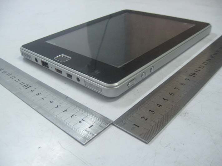
Click to zoom
Application Details
- Equipment Class
- DTS - Digital Transmission System
- Date of Grant
- Jul 10, 2011
- Application Purpose
- Original Equipment
- Date of Application
- Jul 10, 2011
- Equipment Note
- MID
- Frequency Range
- 2422.00000000 - 2452.00000000
- Country
- China
Documents & Files
Document Text
Text extracted from the exhibit documents filed with the FCC. Open a document above to read the original.
Users Manual
Android 2.2 User Manual Directory----------------------------------------------------1 1.Use statement-------------------------------------------1 2.Appearance Description--------------------------------2 2.1 Overall structure----------------------------------2 2.2 Buttons and faucets----------------------------------3-6 3. The description of menu interface-------------------6 3.1 Desktop description-----------------------------------6 3.2 Status Bar Description -------------------------------7 4.Basic set of equipment ---------------------------------8 4.1 Wireless Control --------------------------------------8-9 4.2 Sound and display--------------------------------9-10 4.3 Security and location-----------------------------10 4.4 Date and time-------------------------------------11 4.5 Locate and text------------------------------------12 4.6 Battery Charging----------------------------------12 5. Software installation and management-------------12 5.1 Browser-------------------------------------------12-13 5.2 E-mail----------------------------------------------13 5.3 Google Map --------------------------------------13-14 5.4 Alarm clock ---------------------------------------14-15 5.5 The procedure of using HDMI-------------------15 5.6 The procedure of connecting the tablet PC with computer---------------------------------------------------15 6. O / I File Manager -----------------------------------16 7.FAQ--------------------------------------------------------17 7.1 Can not open the media player---------------------17 7.2 Screen flashing----------------------------------------17 7.3 Headphones can not hear sound-------------------17 7.4 Can not copy the file---------------------------------17 1 1. Use statement Statement: The company are committed to quality innovation and continual improvement of software. If the final version of products has any differences from the description of the user guide, please subject to the final product .Thank you. 2. Appearance Description 2.1 Overall structure 2 2.2 Buttons and faucets 3 4 5 Note: if system halted, please insert one slender material into the reset key ,then system will shutdown insert an external charger, then charging lamp will turn on; When charging is completed, charging lamp will turn off. 3.The description of menu interface 3.1 Desktop description With Pressing the icon" ", you can enter menu and choose the options you need, such as email settings and so on 6 3.2 Status Bar Description The status bar is located on the top screen On the top screen, it shows the followings from left to right: residual battery, current time, lock, home key, return key, menu key, current time, two volume adjustment keys, return key, home key. 7 4. Basic settings of e-pad devices 4.1 Wireless Control press the set-up" " in the menu page to enter set-up interface WI-FI settings: set up and manage the notice of access point to the wireless .When the icon showed on the right is “ " with gray color, which means WIFI is in the state of close 8 click network notification .When the right icon shows““,it means device is scanning the network that is available. The device will search automatically and add the nearby wi-fi network which can be connected. click wireless network port and then you can connect network. 4.2 Sound and display silent mode: All sound will become silent except for media and alarm The Volume of media: Adjust the volume of media by dragging the move point to right or left Direction: It will change the direction automatically when you rotate the MID 9 Cartoon: It will show cartoon when you open or close a window Brightness: Adjust the brightness of screen by dragging the point to the right or left. Idle screen: There are six kinds of time intervals for your choose for idle screen: 15 seconds,30 seconds,1 minutes,2 minutes,10 minutes and 30 minutes. 4.3 Security and location safety and location: set up my location and password selections, Using of wireless network: you can check the location of application by using wireless network Visible password: it will show your password when you typing them 10 4.4 Date and time Date and time: set up date, time, time zone and format Set up date and time: enter the interface of date setting to set up the date and time Select time zone: enter the interface of time zone to set up the time zone Set up time format: set up the display format of time Choose date format: Choose different display format of date 11 4.5 Locate and text set up the locate (languages and areas),text entry and automatic error correction Select area: There are 54 kinds of languages for choice 4.6 Battery Charging There is a built-in battery, when the electric quantity is low, the system will recommend you to charge Way of charging: connect one end of the adaptor to power socket, connect the other end to the power port of the device. 1, When the indicator light of battery charging turns on, it means device is charging. When the indicator light turns to green. It means battery is fully charged. 2, During the charging period, user can still use the Pc. Note: In the boot of state, .it takes long time for charging. 5. Software installation and management 5.1Browser Click" ” and open the following web page. Start: enter website by inputting web address 12 5.2 E-mail Click E-mail icon” ” and enter the e-mail, You can proceed as follows: 1、 Set an e-mail account 2、 Open a new e-mail 3、 Send and receive e-mails Note: Shortcut menu will popup when clicking the menu button.. 5.3 Google map Click” ” and enter Google Map 13 --Click the zoom icons on the touch screen to zoom in and zoom out images --Drag touch screen, move the image up-and-down and right-and-left Click Menu : --search: search maps by entering address --Line : search drive circuit by entering starting and finishing address --Map mode: three modes for choice, map mode、satellite mode and traffic mode. --My position: Find out my current location by setting up "My Location" --more: mo…
Text truncated - open the document above for the full version.
Block Diagram
5 5 4 4 3 3 2 2 1 1 DD CC BB AA Title SizeDocument NumberRev Date:Sheetof Block V1.4 AML8726-M_MID_Ref_B_3G Custom 110Wednesday, January 05, 2011 Title SizeDocument NumberRev Date:Sheetof Block V1.4 AML8726-M_MID_Ref_B_3G Custom 110Wednesday, January 05, 2011 Title SizeDocument NumberRev Date:Sheetof Block V1.4 AML8726-M_MID_Ref_B_3G Custom 110Wednesday, January 05, 2011 LDO +2.5V DC-DC3 +1.8V DC-DC1 DC-DC2 +1.25V +3.3V Battery 1 cell 3.7V DC_IN 5V 3A DCDC Charger PWR_EN PWR_EN PWR_EN PWR_EN DDRII 2 PCS 64Mx16bit OTG 8bitx3 DE,CLK LCD 7' HSD 800X600 Linux Debug SDIO WIFI ADC_KEY VBAT_DET Option for RES touch IR Codec GPIO MOTOR etc. TF CARD HDMI JACK NAND & NOR SPI Nor For Boot 2PCS NAND with TSOP-48 Core CPU DAC/USB/SATA MODULE GPIO,NAND,LCD... DDRII&Codec VCCx2_EN VCC5V USB,HDMI VGH,VGL,AVDD G Sensor Magnetic Sensor CAP/RES TOUCH 24MHz32.768KHz RTC LDO +3.3VRTC POWER 1、DDRII can be used 2 PCS 64Mx16bit,2 PCS 128Mx16bit,4 PCS 128Mx8bit,8 PCS 256Mx4bit.Recommand 2 PCS 64Mx16bit. 2、Many NAND types are available(TSOP-48 or LGA52 package). You can use two NANDs (4 CE total) and 1 PCS I-NAND (SDIO interface).This board only reversed for TSOP,If you need,you can add other type package. 3、USB 2.0. USB_A is a OTG type. USB_B is USB_Host only. DDRII Controller DQ0-DQ31,A0-A13,BA0-BA2,WEN,CKE CK/CKN,CSN,RASN,CASN,UDM_A,LDM_A, ODT,LDQS_A/LDQSN_A,UDQS_A/UDQSN_A, UDM_B,LDM_B,LDQS_B/LDQSN_B, UDQS_B/UDQSN_B NAND Controller Support general NAND & I-nand(SDIO) IO_0-IO_7,RB0,RB1,CE0, CE1,REN_WR,WEN_CLK, CLE,ALE.SPI NOR Flash Interface. USB_A OTG VBUS,ID,DP,DM,TXTTUNE USB_B HOST VBUS,DP,DM,TXTTUNE RGB Interface 24bit RGB R0-R7,G0-G7,B0-B7, UART & I2C UART_A,I2C_A UART_B,I2C_B TCON VCOM,CPH1,OEV1,CPV1 OEH,STV1,STH1,BL& LED_CS IRU601/RMII/FEC_A 8bit FEC&8bit ITU601& RMII Interface&GPIOC_0-12 (Can be used for interrupt) SATA Controller RXM/RXP,TXM/TXP,SATA_REXT ADC 6 channel CH0-CH3:for Touch CH4:for ADC_KEY RTC 32.768KHz OSC 24MHz IR Remote JTAG&I2S Codec HS_LEFT&HS_RIGHT LINE_LEFT&LINE_RIGHT CVBS & YPbPr VDAC_R,VDAC_G,VDAC_B (Up to 1080p). CVBS HDMI Interface HPD,SDA,SCL,CEC TX_CKN/TX_CKP,TX_0N/TX_0P, TX_1N/TX_1P,TX_2N/TX_2P RMII&ITU601 &FEC_B 1、RMII Interface 2、ITU601 Interface 3、8bit FEC_B Interface 4、GPIOD_12-23 SDIO Interface SD_A(For SD/MMC/TF Card) GPIO POWER core:1.28V DDRII:1.8V GPIO:3.3V AML8726-M BGA Support up to 128Mx32bit DDRII SDIO & ISO7816 ISO7816 Interface SDIO(can be used for wifi) GP_INPUT 3 GP_Input Demod test point resevered UART 5V@100mA 1.8V@800mA 2.5V@100mA 1.25V@800mA 3.3V@10mA 3.3V@600mA Step Down Step Down Step Down DC-DC4 Step Up CAMERA XX Extended GPIO Application EM660 3.3V XXXXX MAX 1.1A DC-DC6 Step Down PWR_EN VCCx3_EN AVDD:[email protected] DC-DC5 Step Up LED+ Backlight 6.2V@200mA DC-DC6 PWR_EN PWR_EN Step Up V1R1: 1.PAGE4 增加LGA flash(U41)与INAND(U42) 2.PAGE4 FLASH WP增加阻容滤波(R321/C402)。 3.PAGE2 1.2V调压恒流源网络滤波电容C404由0.1uF改成10nF. V1R2: PAGE4 NAND U22 38PIN(地)与3.3V网络短接修正. V1R3: 1.PAGE4 删除DDR 3个test pin和PZQ 地连接;nand 电阻配置说明更正. 2.PAGE6 修改耳机插入侦测HP_IN 连接方式,满足插入“耳麦型插头”时能正常侦测。 3.PAGE3 内置RES Touch ADC通道改留测试点(TP39-TP42),方便layout。 4.PAGE9 NC WIFI/BT Module 有源晶振Y3,默认使用8726M内部STH pin产生32.768K.增加32.768K网络分压电阻layout说明。 5.PAGE2 D3注明使用DDZ9689;NC R96. UPGRADE LIST: V1R4: 1.PAGE3 RTC取消1K串阻 (OSCIN/OUT);C236由33pF改成27pF;R301由NC改成22R;电池电压侦测取电从VCCX2改到VBAT。ADD"U20本体下方增加散热PAD"说明。 2.PAGE5 C304由10nF改成0.1uF.U25改用MP3202. 3.PAGE10 增加备选摄像头广州大凌实业有限公司DC-100628A/200W pixles说明;upgrade友立森摄像头型号为MC-03G04A。 4.PAGE2 增加R180,预防电池误进入保护,增加D22,防止在系统没供电前,DC_IN电压通过DC_DET漏到VCC3.3V;R216改为1.2K/1%;开机检测电路修改。 5.主要器件属性中增加联系方式。 6.HDMI 接电视时,为预防电压漏到MID上:PAGE3 将CPU wifi Module 3.3V取电由HDMI_3.3V改到ADC_3.3VA。NC FB28,Cancle C216; HDMI_3.3V从LDO U9取电.PAGE8增加D24. 7.PAGE9 预留FM电路。 zenithink zenithink
External Photos
Shenzhen Zenithink Technologies Co., Ltd Model: E98 REPORT NO.: STR11068177I-1 FCC PART 15.247 EXHIBIT 2 - EUT EXTERNAL PHOTOGRAPHS EUT View 1 EUT View 2 Shenzhen Zenithink Technologies Co., Ltd Model: E98 REPORT NO.: STR11068177I-1 FCC PART 15.247 EUT View 3 EUT View 4 Shenzhen Zenithink Technologies Co., Ltd Model: E98 REPORT NO.: STR11068177I-1 FCC PART 15.247 EUT View 5
ID Label/Location Info
Shenzhen Zenithink Technologies Co., Ltd Model: E98 REPORT NO.: STR11068177I-1 FCC PART 15.247 EXHIBIT 1- PRODUCT LABELING Proposed FCC ID Label Format FCC ID: ZAXE98 This device complies with Part 15 of the FCC Rules. Operation is subject to the following two conditions: (1) This device may not cause harmful interference, and (2) This device must accept any interference received, including interference that may cause undesired operation. Specifications : Text is Black in color and justified. Labels are printed in indelible ink on permanent adhesive silk-screened onto the EUT or shall be affixed at a conspicuous location on the EUT. Proposed Label Location on EUT FCC ID Label Location
ID Label/Location Info
Shenzhen Zenithink Technologies Co., Ltd Model: E98 REPORT NO.: STR11068177I-1 FCC PART 15.247 EXHIBIT 1- PRODUCT LABELING Proposed FCC ID Label Format FCC ID: ZAXE98 This device complies with Part 15 of the FCC Rules. Operation is subject to the following two conditions: (1) This device may not cause harmful interference, and (2) This device must accept any interference received, including interference that may cause undesired operation. Specifications : Text is Black in color and justified. Labels are printed in indelible ink on permanent adhesive silk-screened onto the EUT or shall be affixed at a conspicuous location on the EUT. Proposed Label Location on EUT FCC ID Label Location
Internal Photos
Shenzhen Zenithink Technologies Co., Ltd Model: E98 REPORT NO.: STR11068177I-1 FCC PART 15.247 EXHIBIT 3 - EUT INTERNAL PHOTOGRAPHS EUT Housing and Board View Solder Board-Component View 1 Shenzhen Zenithink Technologies Co., Ltd Model: E98 REPORT NO.: STR11068177I-1 FCC PART 15.247 Solder Board-Component View 2 Solder Board-Component View 3 Shenzhen Zenithink Technologies Co., Ltd Model: E98 REPORT NO.: STR11068177I-1 FCC PART 15.247 Solder Board-Component View 4 Solder Board-Component View 5 Shenzhen Zenithink Technologies Co., Ltd Model: E98 REPORT NO.: STR11068177I-1 FCC PART 15.247 Solder Board-Component View 6
Operational Description
Circuit Description 1. The AML8726 chip is master micro controller, the oscillator component X1 generated a frequency of 24MHz as base clock frequency, the AML8726 is a center processing unit which the master frequency of running speed is 333MHz, with 128MHz DRAM and 1GB nand flash, and TF card, one USB port for USB disk and one mini USB port for connect to PC. 2. The WiFi module base on 802.11b/g/n WIFI wireless technolgy, the 32.768kHz clock frequency input to WM-BN-BM-01 as base clock frequency, and use the high-frequency from 2412MHz to 2462MHz as carrier frequency for 802.11b/g/n(HT20), the high-frequency from 2422MHz to 2452MHz as carrier frequency for 802.11n(HT40), the CCK, OFDM modulation type be used. 3. The USB disk and TF card all external signal and data input to MCU as program source, playing and display on LCD screen or output to speaker and external display. 4. The work voltage is DC 3.7V, supply by battery, with a DC 5V power adaptor.
Schematics
5 5 4 4 3 3 2 2 1 1 DD CC BB AA CMDATA2 CMDATA5 CMCLK CMDATA1 CAMR_PWDN CMDATA6 CMPCLK CMDATA3 SENSOR_RST 1V8OUT 2V8OUT CMVREF CMDATA0 I2C_SDA I2C_SCL CMHREF CMDATA4 CMDATA7 1V8OUT 2V8OUT VCCx CM_1.8V CM_2.8V CM_2.8V CM_1.8V CM_2.8V CM_2.8VA CM_2.8VCM_2.8VA PWR_EN12 I2C_SCL3,5,6,8 I2C_SDA3,5,6,8 CMDATA23 CMDATA13 CMDATA33 CMDATA03 CMDATA43 CMPCLK3 CMDATA53 CMDATA63 CMDATA73 CMHREF3 CAMR_PWDN3 CMVREF3 CMCLK3 Title SizeDocument NumberRev Date:Sheet of CAMERA V1.4 AML8726-M_MID_Ref_B Custom 1010Friday, December 31, 2010 Title SizeDocument NumberRev Date:Sheet of CAMERA V1.4 AML8726-M_MID_Ref_B Custom 1010Friday, December 31, 2010 Title SizeDocument NumberRev Date:Sheet of CAMERA V1.4 AML8726-M_MID_Ref_B Custom 1010Friday, December 31, 2010 IQ MAX=1uA WHEN VEN=0V. Each LDO 200mA MAX OUTPUT ON:>1.4V;OFF:<0.4V 友立森摄像头:30W pixels/30fps CAMR_PWDN=H into PWR_Down mode CAMERA PART 亦可用广州大凌实业有限公司摄像头 DC-100628A:200W pixels/ 30fps for SVGA&15fps for UXGA. 注意两种摄像头FPC接口定义有所不同。 注意确认摄像头型号与所需机构是否匹配,很多型号都是为指定机构所做。 R295 100K R295 100K U38 PT5128E23F-E U38 PT5128E23F-E EN1 4 VIN 5 EN2 3 OUT2 1 OUT1 6 GND 2 J8 MC-03G04A J8 MC-03G04A NC 24 NC 23 Y2 22 Y1 21 Y3 20 Y0 19 Y4 18 PCLK 17 Y5 16 DGND 15 Y6 14 XCLK 13 Y7 12 DOVDD 11 DVDD 10 HREF 9 PWDN 8 VSYNC 7 RESET 6 SIO_C 5 AVDD 4 SIO_D 3 AGND 2 NC 1 GND 25 GND 26 C387 106 C387 106 C386 104 C386 104 C388 104 C388 104 C389 18P C389 18P C384 106 C384 106 C399 104 C399 104 C390 104 C390 104 C385 106 C385 106 FB50 120R/100MHz_0.3A_0603 FB50 120R/100MHz_0.3A_0603 R294 47R R294 47R zenithink zenithink 5 5 4 4 3 3 2 2 1 1 DD CC BB AA TXC- TXC+ TX0+ TX0- TX1+ TX1- TX2- TX2+ TX_C- TX_C+ TX_0+ TX_0- TX_1+ TX_1- TX_2- TX_2+ HPD DDCSDA DDCSCL GND I2C_SDA I2C_SCLG_SEN G_SENGND GSEN_INT TX2+ TX1+ TX0+ TXC+ HPD DDCSDA TX2- DDCSCL TX1- TX0- TXC- V_SEN I2C_SDA GND I2C_SCLGND GNDGND HDMI_PW HDMI_PW GND VCC3.3V GND VCC3.3V HDMI_PW VCC3.3V HDMI_PWVCC5V TX_C-3 TX_C+3 TX_0-3 TX_0+3 TX_1-3 TX_1+3 TX_2-3 TX_2+3 HDMI_SCL3 HDMI_SDA3 HDMI_HPD3 I2C_SDA3,5,6,10 I2C_SCL3,5,6,10 GSEN_INT3 MOTOR_EN3 I2C_SCL3,5,6,10 I2C_SDA3,5,6,10 Title SizeDocument NumberRev Date:Sheetof HDMI Interface & Sensor V1.4 AML8726-M_MID_Ref Custom 810Friday, December 31, 2010 Title SizeDocument NumberRev Date:Sheet of HDMI Interface & Sensor V1.4 AML8726-M_MID_Ref Custom 810Friday, December 31, 2010 Title SizeDocument NumberRev Date:Sheet of HDMI Interface & Sensor V1.4 AML8726-M_MID_Ref Custom 810Friday, December 31, 2010 G Sensor Far from Speaker, >50mm Far from Power line,>10mm 触力马达OPTIONAL 注意,此处信号为TypeC排列, 和TypeA,B座子信号排列不同 Magnetic Sensor 注意:MMC3140MS封装与MMC3140MR不同 HDMI Spec. +4.8V < PVDD5 < +5.3V layout注意预留MOTOR的摆放位置 TYPE C HDMI I2C ADDRESS:2AH R26822RR26822R C3684.7uFC3684.7uF D24SS14D24SS14 Q18 NC/8050 Q18 NC/8050 1 2 3 R273NC/4.7KR273NC/4.7K FB45120R/100MHz_0.3A_0603FB45120R/100MHz_0.3A_0603 C3690.1uFC3690.1uF U33MMC3140MSU33MMC3140MS C+ 10 C- 9 CAP 4 TEST/NC 5 VDA 3 VDD 6 SDA 7 SCL 8 FM/NC 2 GND 1 EPAD 11 U32 MXC6225XU U32 MXC6225XU INT 1 NC 2 VDD 3 SCL 4 SDA 5 GND 6 C372 104 C372 104 C370 NC/22uF_10V C370 NC/22uF_10V F1 0.5A-SMD1206 F1 0.5A-SMD1206 D16 1N4148W/SOD323 D16 1N4148W/SOD323 1 2 R272NC/10KR272NC/10K C366 1uF C366 1uF CON3 NC/Motor CON3 NC/Motor 1 2 R265 2.2K R265 2.2K R271NC/2.2RR271NC/2.2R FB46120R/100MHz_0.3A_0603FB46120R/100MHz_0.3A_0603 U35 NC/RCLAMP0524P U35 NC/RCLAMP0524P S1 1 S2 2 GND 3 S3 4 S4 5 S4 6 S3 7 GND 8 S2 9 S1 10 R270 10K R270 10K J6 HDMI_C J6 HDMI_C TX2SD1 1 TX2+ 2 TX2- 3 TX1SD2 4 TX1+ 5 TX1- 6 TX0SD3 7 TX0+ 8 TX0- 9 TXCSD4 10 TXC+ 11 TXC- 12 GND_1 13 CEC 14 SCL 15 SDA 16 RSVD 17 +5V 18 HPD 19 GND_2 20 GND_3 21 GND_4 22 GND_5 23 R2691KR2691K R26722RR26722R C371 106 C371 106 U34 NC/RCLAMP0524P U34 NC/RCLAMP0524P S1 1 S2 2 GND 3 S3 4 S4 5 S4 6 S3 7 GND 8 S2 9 S1 10 C367 0.1uF C367 0.1uF C3650.1uFC3650.1uF R266 2.2K R266 2.2K zenithink zenithink 5 5 4 4 3 3 2 2 1 1 DD CC BB AA USB_ID1 SD_CLK SD_D0 SD_D1 SD_D2 SD_CMD SD_D3 SD_CMD SD_D1 SD_CLK SD_D0 SD_D3 SD_D2 CARD_IN CARD_IN D1- D1+ USB_PWR VCC3.3V CARD_VCC VCC3.3V CARD_VCC VCC3.3V USB_PWRVCC5V VCC3.3V GND GND DM13 DP13 VBUS13 ID13 SD_CLK_A3 SD_CMD_A3 SD_D3_A3 SD_D2_A3 SD_D1_A3 SD_D0_A3 ADC_KEY3 CARD_DET/EN3 USB_PWR_CTL3 IR3 Title SizeDocument NumberRev Date:Sheetof Key &IR&USB & Card V1.4 AML8726-M_MID_Ref_B Custom 710Friday, December 31, 2010 Title SizeDocument NumberRev Date:Sheetof Key &IR&USB & Card V1.4 AML8726-M_MID_Ref_B Custom 710Friday, December 31, 2010 Title SizeDocument NumberRev Date:Sheetof Key &IR&USB & Card V1.4 AML8726-M_MID_Ref_B Custom 710Friday, December 31, 2010 需要较少按键时,可以去掉一些按键, 合并阻值。 同时按下多个按键时,检测到最左边 低压按键OK键等特殊按键应当放在 右侧高压端 Close to CPU 根据需要选定封装 0V ESC 0.58V1.286V2.01V2.74V 侧立按键,各按键丝印相应功能。 HOMEVOL+MENUVOL- 可以检测卡的输入及卡电源的控制。 CARD_DET/EN默认为输入, 检测到低电平后(有卡插入), 设为输出可控制卡电源,稳定 后,设为输入,检测是否有卡 插拔的操作。只用单一的卡时, 可以不做电源控制。 Close to Card 限制输出电流 ADC KEY TF CARD USB OTG IR R314 NC/4.7K R0603 R314 NC/4.7K R0603 C358 0.1uF C358 0.1uF K4 Button K4 Button 1 2 3 4 K5 Button K5 Button 1 2 3 4 U36 Remote_Control REMOTEX1.23 U36 Remote_Control REMOTEX1.23 OUT GND VCC U31 TF_SD_SOCKET U31 TF_SD_SOCKET CD/DATA3 2 CMD 3 VDD 4 CLK 5 VSS 6 DATA0 7 DATA1 8 CD 9 G1 10 DATA2 1 G2 11 G3 12 G4 13 R246 4.7K_1% R246 4.7K_1% R25822RR25822R L10 NC/EXD24CD900U L10 NC/EXD24CD900U 1 4 2 3 U30 RT9702CB U30 RT9702CB CE 1 VOUT 5 GND 2 /FLG 3 VIN 4 R25722RR25722R R2644.7KR2644.7K K3 Button K3 Button 1 2 3 4 D14 NC/ESDP D14 NC/ESDP 1 2 R262 4.7K R262 4.7K C318 10uF_10V C0805 C318 10uF_10V C0805 C363 0.1uF C363 0.1uF C364 1UF C364 1UF R25922RR25922R C362NC/10pFC362NC/10pF R249 10K R249 10K R253 4.3K_%1 R253 4.3K_%1 K2 Button K2 Button 1 2 3 4 VBUS D- D+ ID GND CON2 USB Port/Mini-B/5pin/SMD VBUS D- D+ ID GND CON2 USB Port/Mini-B/5pin/SMD 1 2 3 4 5 6 7 8 9 C360 1nF C360 1nF R260 MCB1005S121FBP R260 MCB1005S121FBP C398 nc/10pF C0603 C398 nc/10pF C0603 R2501KR2501K R2391KR2391K R252 2K_%1 R252 2K_%1 C359 1nF C359 1nF R2430RR2430R R315 4.7R R0603 R315 4.7R R0603 R254 16K_%1 R254 16K_%1 R244 2.2K R244 2.2K R251 1K_%1 R251 1K_%1 D15 NC/ESDP D15 NC/ESDP 1 2 K1 Button K…
Text truncated - open the document above for the full version.
Test Report
Shenzhen Zenithink Technologies Co., Ltd Model: E98 REPORT NO.: STR11068177I-1 PAGE 1 OF 80 FCC PART 15.247 FCC Part 15C Measurement and Test Report For Shenzhen Zenithink Technologies Co., Ltd 2nd Floor, Building M-3, Maqueling Industrial zone, Nanshan District, Shenzhen, P.R. China FCC ID: ZAXE98 Report Concerns: Original Report Equipment Type: MID Model: E98 Report No.: STR11068177I-1 Test Date: 2011-06-20 to 2011-07-05 Issue Date: 2011-07-11 Tested By: Jason Chen / Engineer Reviewed By: Lahm Peng / EMC Manager Approved & Authorized By: Jandy so / PSQ Manager Prepared By: SEM.Test Compliance Service Co., Ltd 3/F, Jinbao Commerce Building, Xin'an Fanshen Road, Bao'an District, Shenzhen, P.R.C.(518101) Tel.: +86-755-33663308 Fax.: +86-755-33663309 Website: www.semtest.com.cn Note: This test report is limited to the above client company and the product model only. It may not be duplicated without prior permitted by SEM.Test Compliance Service Co., Ltd . Shenzhen Zenithink Technologies Co., Ltd Model: E98 REPORT NO.: STR11068177I-1 PAGE 2 OF 80 FCC PART 15.247 TABLE OF CONTENTS 1. GENERAL INFORMATION ...................................................................................................................................3 1.1 PRODUCT DESCRIPTION FOR EQUIPMENT UNDER TEST (EUT)...............................................................................3 1.2 TEST STANDARDS...................................................................................................................................................3 1.3 TEST METHODOLOGY.............................................................................................................................................3 1.4 TEST FACILITY.......................................................................................................................................................4 1.5 EUT EXERCISE SOFTWARE....................................................................................................................................4 1.6 ACCESSORIES EQUIPMENT LIST AND DETAILS.......................................................................................................4 1.7 EUT CABLE LIST AND DETAILS.............................................................................................................................4 2. SUMMARY OF TEST RESULTS ...........................................................................................................................5 3. CONDUCTED EMISSIONS ....................................................................................................................................6 3.1 MEASUREMENT UNCERTAINTY..............................................................................................................................6 3.2 TEST EQUIPMENT LIST AND DETAILS.....................................................................................................................6 3.3 TEST PROCEDURE...................................................................................................................................................6 3.4 BASIC TEST SETUP BLOCK DIAGRAM.....................................................................................................................6 3.5 ENVIRONMENTAL CONDITIONS..............................................................................................................................7 3.6 SUMMARY OF TEST RESULTS/PLOTS......................................................................................................................7 3.7 CONDUCTED EMISSIONS TEST DATA......................................................................................................................7 4. §15.203 - ANTENNA REQUIREMENT................................................................................................................10 4.1 STANDARD APPLICABLE.......................................................................................................................................10 4.2 TEST RESULT........................................................................................................................................................10 5. POWER SPECTRAL DENSITY ...........................................................................................................................11 5.1 STANDARD APPLICABLE.......................................................................................................................................11 5.2 TEST EQUIPMENT LIST AND DETAILS...................................................................................................................11 5.3 TEST PROCEDURE.................................................................................................................................................11 5.4 ENVIRONMENTAL CONDITIONS............................................................................................................................11 5.5 SUMMARY OF TEST RESULTS/PLOTS....................................................................................................................12 6. 6-DB BANDWIDTH ................................................................................................................................................19 6.1 STANDARD APPLICABLE.......................................................................................................................................19 6.2 TEST EQUIPMENT LIST AND DETAILS...................................................................................................................19 6.3 TEST PROCEDURE.................................................................................................................................................19 6.4 ENVIRONMENTAL CONDITIONS............................................................................................................................19 6.5 SUMMARY OF TEST RESULTS/PLOTS..…
Text truncated - open the document above for the full version.
Test Setup Photos
Shenzhen Zenithink Technologies Co., Ltd Model: E98 REPORT NO.: STR11068177I-1 FCC PART 15.247 EXHIBIT 4 - TEST SETUP PHOTOGRAPHS Radiation Emission Test Setup (30MHz to 1GHz) Radiation Emission Test Setup (Above 1GHz)
Contact Information
Applicant
Ani Yi(Sales)
Test Firm
SEM.Test Compliance Service Co., Ltd.Jandy So
Technical Specifications
| # | Rule Parts | Frequency Range | Power Output |
|---|---|---|---|
| 2 | 15C | 2.42 GHz - 2.45 GHz | 8.00 mW |
Other Applications from Shenzhen Zenithink Technologies Co., Ltd.
ZAXZT280-C91
Oct 11, 2011MID
Equipment Class
DTS - Digital Transmission System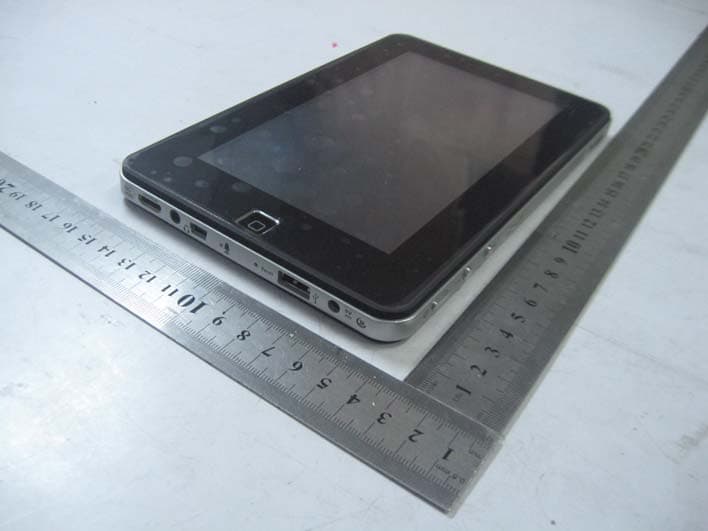
ZAXZT1807A
Mar 29, 2011MID
Equipment Class
DTS - Digital Transmission System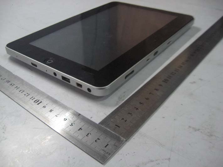
Mar 16, 2011
Equipment Class
JBP - Part 15 Class B Computing Device Peripheral