ZQ6-AP6356SDXXWLAN module for 802.11abgn(2x2) + 11ac+BT4.1
AMPAK Technology Inc.
Click to zoom
Application Details
- Equipment Class
- DTS - Digital Transmission System
- Date of Grant
- Dec 30, 2015
- Application Purpose
- Original Equipment
- Date of Application
- Dec 29, 2015
- Equipment Note
- WLAN module for 802.11abgn(2x2) + 11ac+BT4.1
- Frequency Range
- 2402.00000000 - 2480.00000000
- Company
- AMPAK Technology Inc.
- Country
- Taiwan
Documents & Files
Document Text
Text extracted from the exhibit documents filed with the FCC. Open a document above to read the original.
Users Manual
AMPAK Technology Inc. www.ampak.com.tw Proprietary & Confidential Information i Doc. NO: AMPAK AP6356SDXX Evaluation Kits User manual Version 1.0 Revision History Date Revision Content Revised By Version 2015/12/28 Initial released Aron 1.0 AMPAK Technology Inc. www.ampak.com.tw Proprietary & Confidential Information Doc. NO: 1 Federal Communication Commission Interference Statement This device complies with Part 15 of the FCC Rules. Operation is subject to the following two conditions: (1) This device may not cause harmful interference, and (2) this device must accept any interference received, including interference that may cause undesired operation. This equipment has been tested and found to comply with the limits for a Class B digital device, pursuant to Part 15 of the FCC Rules. These limits are designed to provide reasonable protection against harmful interference in a residential installation. This equipment generates, uses and can radiate radio frequency energy and, if not installed and used in accordance with the instructions, may cause harmful interference to radio communications. However, there is no guarantee that interference will not occur in a particular installation. If this equipment does cause harmful interference to radio or television reception, which can be determined by turning the equipment off and on, the user is encouraged to try to correct the interference by one of the following measures: - Reorient or relocate the receiving antenna. - Increase the separation between the equipment and receiver. - Connect the equipment into an outlet on a circuit different from that to which the receiver is connected. - Consult the dealer or an experienced radio/TV technician for help. FCC Caution: Any changes or modifications not expressly approved by the party responsible for compliance could void the user's authority to operate this equipment. This transmitter must not be co-located or operating in conjunction with any other antenna or transmitter. AMPAK Technology Inc. www.ampak.com.tw Proprietary & Confidential Information Doc. NO: 2 Radiation Exposure Statement: This equipment complies with FCC radiation exposure limits set forth for an uncontrolled environment. This equipment should be installed and operated with minimum distance 20cm between the radiator & your body. This device is intended only for OEM integrators under the following conditions: 1) The antenna must be installed such that 20 cm is maintained between the antenna and users, and 2) The transmitter module may not be co-located with any other transmitter or antenna. As long as 2 conditions above are met, further transmitter test will not be required. However, the OEM integrator is still responsible for testing their end-product for any additional compliance requirements required with this module installed IMPORTANT NOTE: In the event that these conditions can not be met (for example certain laptop configurations or co-location with another transmitter), then the FCC authorization is no longer considered valid and the FCC ID can not be used on the final product. In these circumstances, the OEM integrator will be responsible for re-evaluating the end product (including the transmitter) and obtaining a separate FCC authorization. End Product Labeling This transmitter module is authorized only for use in device where the antenna may be installed such that 20 cm may be maintained between the antenna and users. The final end product must be labeled in a visible area with the following: “Contains FCC ID:ZQ6-AP6356SDXX”. The grantee's FCC ID can be used only when all FCC compliance requirements are met. Manual Information To the End User The OEM integrator has to be aware not to provide information to the end user regarding how to install or remove this RF module in the user’s manual of the end product which integrates this module. The end user manual shall include all required regulatory information/warning as show in this manual. AMPAK Technology Inc. www.ampak.com.tw Proprietary & Confidential Information Doc. NO: 3 1. AP6356SDXX Evaluation Board Introduction AP6356SDXX Evaluation board (EVB) likes as figure1. That is designed for IEEE802.11 a/b/g/n/ac 2x2 WLAN with integrated Bluetooth. It is subject to provide a convenient environment for customer’s verification on WiFi or Bluetooth function. There are many controller pins and reserved GPIO on Evaluation board which describes as below. Figure1. Top view of AP6356SDXX EVB Interface highlights: 1. U1: AP6356SDXX SIP module. 2. J1: UART interface connects with UART transport board for BT. 3. J80: PCIE interface connects with PCIE transport board for WIFI. 4. J3: Enable(H) or disable(L) Bluetooth and WiFi function. 5. J4: PCIE interface strapping option 6. J5: 5V DC adaptor input connector. 7. J6: 3V3 RF/ VBAT / WL_VIO / BT_VIO for main system I/O power path. 8. J7/J9: 5V DC mini USB input connector. 9. J10: GPIO_2 (input/output) and GPIO_3 (input/output) 10. J11: WL_VIO power path for 1V8 or 3V3 selection. 11. A1: I-PEX connector let RF signal in/out path, you could connect with RF cable or J10 J4 J3 J1 A2 U1 A1 J80 ct2 ct3 ct4 J7 J5 J9 J11 J6 ct1 AMPAK Technology Inc. www.ampak.com.tw Proprietary & Confidential Information Doc. NO: 4 Dipole antenna. 12. A2: I-PEX connector let RF signal in/out path, you could connect with RF cable or Dipole antenna. 13. Ct1-Ct4: WLAN and BT control pins, strongly recommended WL_H_WAKE(IRQ) connected to MCU. 2. WiFi function verification step WIFI PCIe: PCIe interface definition as below J80 dip connector and this should be used 3.3V for PCIe voltage. Figure3. WiFi verification connection interface to Host PCIE Hardware Setup: Refer to Figure3 PCIE pin definition connects the J80 interface of AP6356SDXX evaluation board to Host PCIE control interface. Connects an external antenna at I-PEX connector on the evaluation board. Note to the VDDIO voltage level should be the same with GPIO voltage level of Host CPU. (VDDIO 3.3V or…
Text truncated - open the document above for the full version.
External Photos
Page 1 CONSTRUCTION PHOTOS OF EUT
Internal Photos
Page 2 Page 3 Page 4
RF Exposure Info
Report No.: SA150821C10A Page No. 1 / 5 Report Format Version: 6.1.1 Reference No.: 151228C08 RF Exposure Report Report No.: SA150821C10A FCC ID: ZQ6-AP6356SDXX Test Model: AP6356SD Received Date: Aug. 21, 2015 Test Date: Nov. 25 ~ Dec. 26, 2015 Issued Date: Dec. 28, 2015 Applicant: AMPAK Technology Inc. Address: 3F, No.1, Jen AI Road, Hsinchu Industrial Park, Hsinchu, Taiwan, 30352 Issued By: Bureau Veritas Consumer Products Services (H.K.) Ltd., Taoyuan Branch Lab Address: No. 47-2, 14th Ling, Chia Pau Vil., Lin Kou Dist., New Taipei City, Taiwan, R.O.C. Test Location: No. 19, Hwa Ya 2nd Rd., Wen Hwa Vil., Kwei Shan Dist., Taoyuan City 33383, TAIWAN (R.O.C.) This report is for your exclusive use. Any copying or replication of this report to or for any other person or entity, or use of our name or trademark, is permitted only with our prior written permission. This report sets forth our findings solely with respect to the test samples identified herein. The results set forth in this report are not indicative or representative of the quality or characteristics of the lot from which a test sample was taken or any similar or identical product unless specifically and expressly noted. Our report includes all of the tests requested by you and the results thereof based upon the information that you provided to us. You have 60 days from date of issuance of this report to notify us of any material error or omission caused by our negligence, provided, however, that such notice shall be in writing and shall specifically address the issue you wish to raise. A failure to raise such issue within the prescribed time shall constitute your unqualified acceptance of the completeness of this report, the tests conducted and the correctness of the report contents. Unless specific mention, the uncertainty of measurement has been explicitly taken into account to declare the compliance or non-compliance to the specification. The report must not be used by the client to claim product certification, approval, or endorsement by TAF or any government agencies. Report No.: SA150821C10A Page No. 2 / 5 Report Format Version: 6.1.1 Reference No.: 151228C08 Table of Contents Release Control Record .................................................................................................................................. 3 1 Certificate of Conformity ...................................................................................................................... 4 2 RF Exposure .......................................................................................................................................... 5 2.1 Limits for Maximum Permissible Exposure (MPE) .............................................................................. 5 2.2 MPE Calculation Formula ................................................................................................................... 5 2.3 Classification ....................................................................................................................................... 5 3 Calculation Result Of Maximum Conducted Power .......................................................................... 5 Report No.: SA150821C10A Page No. 3 / 5 Report Format Version: 6.1.1 Reference No.: 151228C08 Release Control Record Issue No. Description Date Issued SA150821C10 Original release Dec. 28, 2015 Report No.: SA150821C10A Page No. 4 / 5 Report Format Version: 6.1.1 Reference No.: 151228C08 1 Certificate of Conformity Product: WLAN module for 802.11abgn(2x2) + 11ac + BT4.1 Brand: Ampak Test Model: AP6356SD Sample Status: Engineering Sample Applicant: AMPAK Technology Inc. Test Date: Nov. 25 ~ Dec. 26, 2015 Standards: FCC Part 2 (Section 2.1091) KDB 447498 D01 (October 23, 2015) IEEE C95.1 The above equipment has been tested by Bureau Veritas Consumer Products Services (H.K.) Ltd., Taoyuan Branch, and found compliance with the requirement of the above standards. The test record, data evaluation & Equipment Under Test (EUT) configurations represented herein are true and accurate accounts of the measurements of the sample’s EMC characteristics under the conditions specified in this report. Prepared by : , Date:Dec. 28, 2015 Celine Chou / Specialist Approved by : , Date:Dec. 28, 2015 Ken Liu / Senior Manager Report No.: SA150821C10A Page No. 5 / 5 Report Format Version: 6.1.1 Reference No.: 151228C08 2 RF Exposure 2.1 Limits for Maximum Permissible Exposure (MPE) Frequency Range (MHz) Electric Field Strength (V/m) Magnetic Field Strength (A/m) Power Density (mW/cm 2 ) Average Time (minutes) Limits For General Population / Uncontrolled Exposure 300-1500 ... ... F/1500 30 1500-100,000 ... ... 1.0 30 F = Frequency in MHz 2.2 MPE Calculation Formula Pd = (Pout*G) / (4*pi*r 2 ) where Pd = power density in mW/cm 2 Pout = output power to antenna in mW G = gain of antenna in linear scale Pi = 3.1416 R = distance between observation point and center of the radiator in cm 2.3 Classification The antenna of this product, under normal use condition, is at least 20cm away from the body of the user. So, this device is classified as Mobile Device. 3 Calculation Result Of Maximum Conducted Power EUT Function Frequency Band (MHz) TX Function Max Power (dBm) Antenna Gain (dBi) Distance (cm) Power Density (mW/cm2) Limit (mW/cm2) WLAN 2412-2462 1TX 14.15 3.51 20 0.012 1 2TX 14.91 6.51 20 0.028 1 5180-52402TX 12.43 8.51 20 0.025 1 5745-58252TX 12.69 8.51 20 0.026 1 Bluetooth LE 2402-2480 1TX 7.25 3.51 20 0.002 1 Bluetooth EDR 2402-24801TX 7.84 3.51 20 0.003 1 Note: 2.4GHz: Directional gain = 3.5dBi + 10log(2) = 6.51dBi 5GHz: Directional gain = 5.5dBi + 10log(2) = 8.51dBi * Both of the 2.4GHz and 5GHz can not transmit simultaneously ---END---
Test Report
Report No.: RF150821C10-2 Page No. 1 / 32 Report Format Version: 6.1.1 FCC Test Report Report No.: RF150821C10-2 FCC ID: ZQ6-AP6356SDXX Test Model: AP6356SD Received Date: Aug. 21, 2015 Test Date: Dec. 24 ~ Dec. 26, 2015 Issued Date: Dec. 28, 2015 Applicant: AMPAK Technology Inc. Address: 3F, No.1, Jen AI Road, Hsinchu Industrial Park, Hsinchu, Taiwan, 30352 Issued By: Bureau Veritas Consumer Products Services (H.K.) Ltd., Taoyuan Branch Lab Address: No. 47-2, 14th Ling, Chia Pau Vil., Lin Kou Dist., New Taipei City, Taiwan, R.O.C. Test Location: No.19, Hwa Ya 2nd Rd., Wen Hwa Vil., Kwei Shan Dist., Taoyuan City 33383, TAIWAN (R.O.C.) This report is for your exclusive use. Any copying or replication of this report to or for any other person or entity, or use of our name or trademark, is permitted only with our prior written permission. This report sets forth our findings solely with respect to the test samples identified herein. The results set forth in this report are not indicative or representative of the quality or characteristics of the lot from which a test sample was taken or any similar or identical product unless specifically and expressly noted. Our report includes all of the tests requested by you and the results thereof based upon the information that you provided to us. You have 60 days from date of issuance of this report to notify us of any material error or omission caused by our negligence, provided, however, that such notice shall be in writing and shall specifically address the issue you wish to raise. A failure to raise such issue within the prescribed time shall constitute your unqualified acceptance of the completeness of this report, the tests conducted and the correctness of the report contents. Unless specific mention, the uncertainty of measurement has been explicitly taken into account to declare the compliance or non-compliance to the specification. This report should not be used by the client to claim product certification, approval, or endorsement by TAF or any government agencies. Report No.: RF150821C10-2 Page No. 2 / 32 Report Format Version: 6.1.1 Table of Contents Release Control Record .................................................................................................................................. 4 1 Certificate of Conformity ...................................................................................................................... 5 2 Summary of Test Results ..................................................................................................................... 6 2.1 Measurement Uncertainty ................................................................................................................... 6 2.2 Modification Record ............................................................................................................................ 6 3 General Information .............................................................................................................................. 7 3.1 General Description of EUT ................................................................................................................ 7 3.2 Description of Test Modes ................................................................................................................... 7 3.2.1 Test Mode Applicability and Tested Channel Detail ............................................................................. 8 3.3 Description of Support Units ............................................................................................................. 10 3.3.1 Configuration of System under Test .................................................................................................. 10 3.4 General Description of Applied Standards ........................................................................................ 10 4 Test Types and Results ....................................................................................................................... 11 4.1 Radiated Emission and Bandedge Measurement .............................................................................. 11 4.1.1 Limits of Radiated Emission and Bandedge Measurement ............................................................... 11 4.1.2 Test Instruments ................................................................................................................................ 12 4.1.3 Test Procedures ................................................................................................................................. 13 4.1.4 Deviation from Test Standard ............................................................................................................ 13 4.1.5 Test Set Up ........................................................................................................................................ 14 4.1.6 EUT Operating Conditions ................................................................................................................. 14 4.1.7 Test Results ....................................................................................................................................... 15 4.2 Conducted Emission Measurement .................................................................................................. 19 4.2.1 Limits of Conducted Emission Measurement .................................................................................... 19 4.2.2 Test Instruments ................................................................................................................................ 19 4.2.3 Test Procedures ................................................................................................................................. 20 4.2.4 Deviation from Test Standard ............................................................................................................ 20 4.2.5 Test Setup .......................................…
Text truncated - open the document above for the full version.
Test Report
Report No.: RF150821C10 Page No. 1 / 53 Report Format Version: 6.1.1 FCC Test Report Report No.: RF150821C10 FCC ID: ZQ6-AP6356SDXX Test Model: AP6356SD Received Date: Aug. 21, 2015 Test Date: Nov. 25 ~ Dec. 26, 2015 Issued Date: Dec. 28, 2015 Applicant: AMPAK Technology Inc. Address: 3F, No.1, Jen AI Road, Hsinchu Industrial Park, Hsinchu, Taiwan, 30352 Issued By: Bureau Veritas Consumer Products Services (H.K.) Ltd., Taoyuan Branch Lab Address: No. 47-2, 14th Ling, Chia Pau Vil., Lin Kou Dist., New Taipei City, Taiwan, R.O.C. Lab Address: No.19, Hwa Ya 2nd Rd., Wen Hwa Vil., Kwei Shan Dist., Taoyuan City 33383, TAIWAN (R.O.C.) This report is for your exclusive use. Any copying or replication of this report to or for any other person or entity, or use of our name or trademark, is permitted only with our prior written permission. This report sets forth our findings solely with respect to the test samples identified herein. The results set forth in this report are not indicative or representative of the quality or characteristics of the lot from which a test sample was taken or any similar or identical product unless specifically and expressly noted. Our report includes all of the tests requested by you and the results thereof based upon the information that you provided to us. You have 60 days from date of issuance of this report to notify us of any material error or omission caused by our negligence, provided, however, that such notice shall be in writing and shall specifically address the issue you wish to raise. A failure to raise such issue within the prescribed time shall constitute your unqualified acceptance of the completeness of this report, the tests conducted and the correctness of the report contents. Unless specific mention, the uncertainty of measurement has been explicitly taken into account to declare the compliance or non-compliance to the specification. This report should not be used by the client to claim product certification, approval, or endorsement by TAF or any government agencies. Report No.: RF150821C10 Page No. 2 / 53 Report Format Version: 6.1.1 Table of Contents Release Control Record .................................................................................................................................. 4 1 Certificate of Conformity ...................................................................................................................... 5 2 Summary of Test Results ..................................................................................................................... 6 2.1 Measurement Uncertainty ................................................................................................................... 6 2.2 Modification Record ............................................................................................................................ 6 3 General Information .............................................................................................................................. 7 3.1 General Description of EUT ................................................................................................................ 7 3.2 Description of Test Modes ................................................................................................................... 8 3.2.1 Test Mode Applicability and Tested Channel Detail ............................................................................. 9 3.3 Duty Cycle of Test Signal ................................................................................................................... 11 3.4 Description of Support Units ............................................................................................................. 12 3.4.1 Configuration of System under Test .................................................................................................. 12 3.5 General Description of Applied Standards ........................................................................................ 12 4 Test Types and Results ...................................................................................................................... 13 4.1 Radiated Emission and Bandedge Measurement ............................................................................. 13 4.1.1 Limits of Radiated Emission and Bandedge Measurement .............................................................. 13 4.1.2 Test Instruments ................................................................................................................................ 14 4.1.3 Test Procedures ................................................................................................................................. 15 4.1.4 Deviation from Test Standard ............................................................................................................ 15 4.1.5 Test Set Up ........................................................................................................................................ 16 4.1.6 EUT Operating Conditions ................................................................................................................. 16 4.1.7 Test Results ....................................................................................................................................... 17 4.2 Conducted Emission Measurement .................................................................................................. 30 4.2.1 Limits of Conducted Emission Measurement .................................................................................... 30 4.2.2 Test Instruments ................................................................................................................................ 30 4.2.3 Test Procedures ................................................................................................................................. 31 4.2.4 Deviation from Test Standard ..............................…
Text truncated - open the document above for the full version.
Test Setup Photos
1 PHOTOGRAPHS OF THE TEST CONFIGURATION Conducted Emission Test 2 Radiated Emissions below 1 GHz Test (Z-Plane) 3 Radiated Emissions below 1 GHz Test (Y-Plane) 4 Radiated Emissions above 1 GHz Test (Z-Plane) 5 Radiated Emissions above 1 GHz Test (Y-Plane)
Contact Information
Applicant
Changyi Tsai(Manager)
Test Firm
Bureau Veritas CPS (H.K.) Ltd., Taoyuan BranchRichard Chen
Technical Specifications
| # | Rule Parts | Frequency Range | Power Output |
|---|---|---|---|
| 2 | 15C | 2.40 GHz - 2.48 GHz | 5.00 mW |
Other Applications from AMPAK Technology Inc.
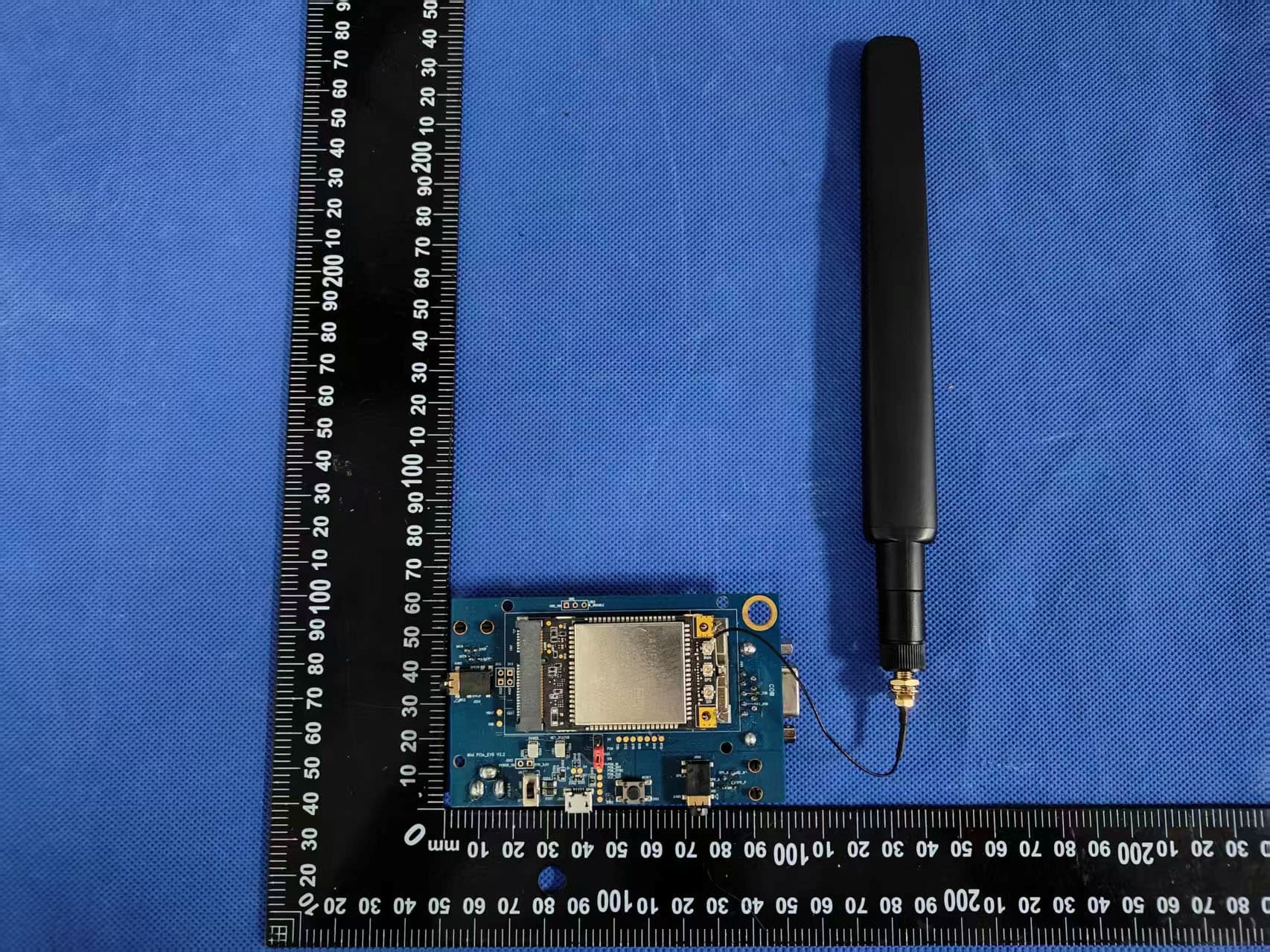
ZQ6-AC4207-NA
May 12, 2026AC4207_NA
Equipment Class
PCB - PCS Licensed TransmitterZQ6-AP6684PL
May 08, 2026AP6684PL
Equipment Class
6XD - 15E 6 GHz Low Power Indoor Client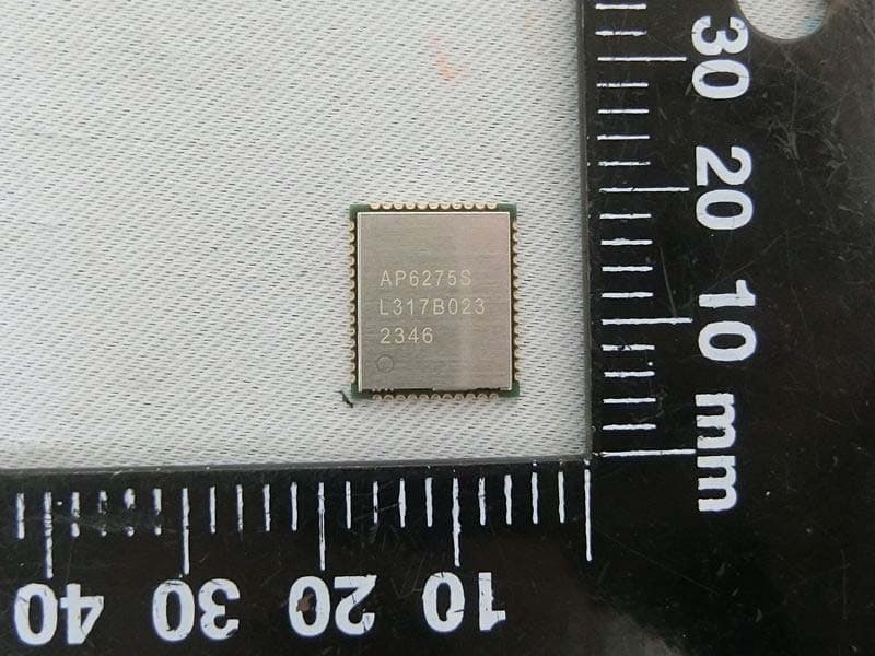
ZQ6-AP6275S
Oct 03, 2024Wi-Fi/Bluetooth Module
Equipment Class
DTS - Digital Transmission System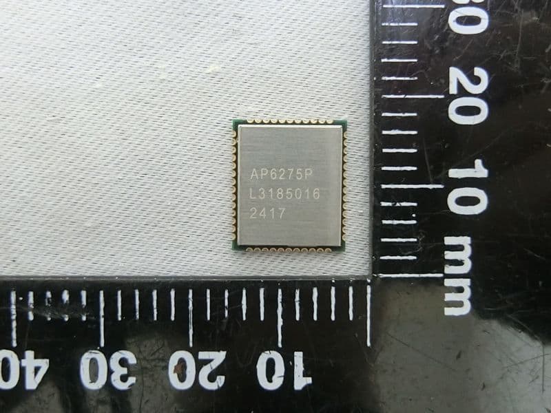
ZQ6-AP6275P
Sep 08, 2024Wi-Fi/Bluetooth Module
Equipment Class
DSS - Part 15 Spread Spectrum Transmitter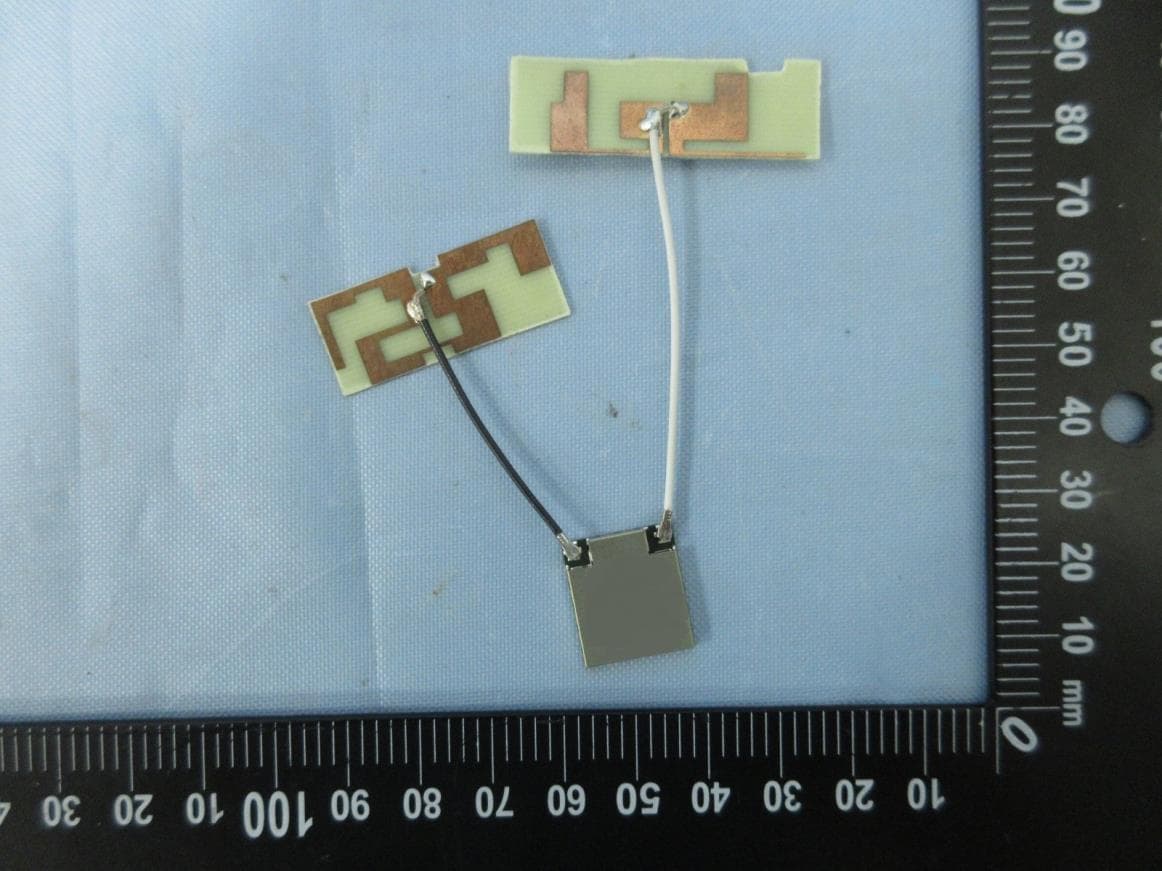
ZQ6-AP6398XU
Aug 16, 2020Wi-Fi and Bluetooth module
Equipment Class
DSS - Part 15 Spread Spectrum Transmitter