2ACEVS84.5 INCH SMARTPHONE
IED CONEXION VIRTUAL S.A. DE C.V.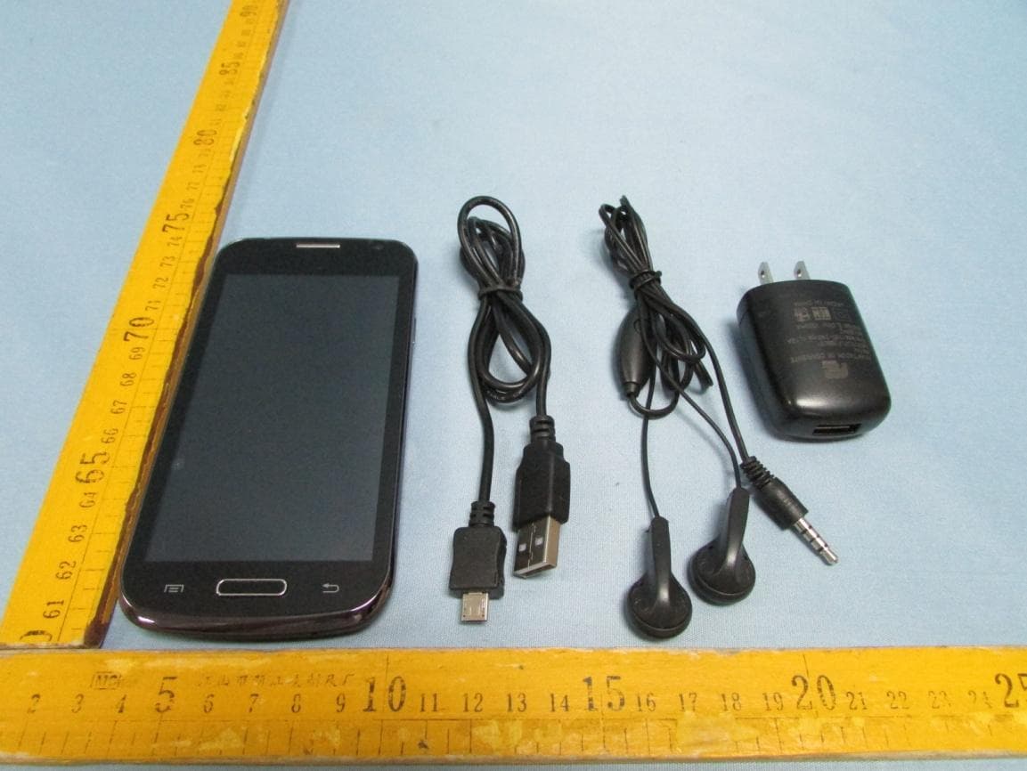
Click to zoom
Application Details
- Equipment Class
- PCE - PCS Licensed Transmitter held to ear
- Date of Grant
- Jul 06, 2014
- Application Purpose
- Original Equipment
- Date of Application
- Jul 02, 2014
- Equipment Note
- 4.5 INCH SMARTPHONE
- Frequency Range
- 1852.40000000 - 1907.40000000
- Country
- Mexico
Documents & Files
Document Text
Text extracted from the exhibit documents filed with the FCC. Open a document above to read the original.
Users Manual
QUANTUM S8 user manual Content 1 General Information.................................................................................................................................................4 1.1 Profile.............................................................................................................................................................. 4 1.2 Safety warning and Attentions ........................................................................................................................ 4 2 Your phone.................................................................................................................................................................7 2.1 Phone overview............................................................................................................................................... 7 2.2 Functions of Keys ........................................................................................................................................... 7 2.3 Functions of icons........................................................................................................................................... 8 3 Getting started...........................................................................................................................................................8 3.1 Installing the SIM Card and the Battery ......................................................................................................... 8 3.2 Charging the Battery ....................................................................................................................................... 9 3.3 Linking to the Networks and devices.............................................................................................................11 3.4 Using the touch screen .................................................................................................................................. 12 3.5 Using the onscreen keypad ........................................................................................................................... 13 3.6 Dialing Calls ................................................................................................................................................. 14 4 Using the Menus......................................................................................................................................................15 4.1 Browser......................................................................................................................................................... 15 4.2 Calculator...................................................................................................................................................... 17 4.3 Calendar ........................................................................................................................................................ 18 4.4 Camera .......................................................................................................................................................... 19 4.5 Clock............................................................................................................................................................. 19 4.6 Downloads .................................................................................................................................................... 19 4.7 Email............................................................................................................................................................. 20 4.8 File manager.................................................................................................................................................. 21 4.9 Flash player settings...................................................................................................................................... 21 4.10 FM Radio ...................................................................................................................................................... 21 4.11 Gallery .......................................................................................................................................................... 21 4.12 Messaging ..................................................................................................................................................... 21 4.13 Music ............................................................................................................................................................ 22 4.14 People............................................................................................................................................................ 23 4.15 Phone ............................................................................................................................................................ 24 4.16 Play store....................................................................................................................................................... 24 4.17 Search............................................................................................................................................................ 24 4.18 Settings.......................................................................................................................................................... 24 4.19 SIM Toolkit................................................................................................................................................... 28 4.20 Sound Recorder............................................................................................................................................. 28 4.21 To Do ...............................................................................................................................…
Text truncated - open the document above for the full version.
Cover Letter(s)
IED CONEXION VIRTUAL S.A DE C.V Rio Tiber # 103 Int 502 Colonia DF CP: 06500 Cuauhtemoc Mexico Date: July 1, 2014 Statement We, IED CONEXION VIRTUAL S.A DE C.V, states that our device, FCC ID: 2ACEVS8. According to FCC Part 2.925 rule, the label will put under the battery inside the battery compartment since limitation of the size, and it is visible to the users as they purchase the products and install the battery. Sincerely yours,
Cover Letter(s)
IED CONEXION VIRTUAL S.A DE C.V Federal Communications Commission Authorization and Evaluation Division 1435 Oakland Mills Road Columbia, MD 21046 Date: 2014.06.15 SUBJECT: FCC Application for FCC ID: 2ACEVS8 To Whom It May Concern: I, the undersigned, hereby attest to the fact that I will apply the Declaration of Conformity procedure to the class B computer peripheral portion of this composite device. I understand the following FCC requirements: 1. Devices subject to the DoC procedure are required to be tested to show compliance with the FCC technical regulations by a recognized accredited testing laboratory. The testing laboratory must be accredited by a Commission approved accreditation body or designated under the terms of a government-to-government Mutual Recognition Agreement (MRA). A listing of those accredited testing laboratories that have been recognized by the Commission is published on the FCC Webpage: https://apps.fcc.gov/oetcf/eas/reports/TestFirmSearch.cfm (Select the "accredited" option to search for FCC recognized accredited test firms.) 2. Test facilities located in countries, where the U.S. does not have an operational Telcom MRA are not recognized by the FCC to test for the DoC procedure. 3. Pt 2.1077 contains the list of information that must be included in the Declaration of Conformity, which must be supplied with each product sold. The DoC compliance info shall be included in the User’s Manual or as a separate sheet. The info must contain the name, address, and phone number of the responsible party, which must be located within the United States. According to 2.909(c)(2), the responsible party is either the Manufacturer or if the product is imported the Importer. Regards, Signature:(Must be signed by the person that is listed on the FCC Website)
Cover Letter(s)
Page 1 of 1 Test Lab Attestation Letter Date of Test: 2014‐06‐17to 2014‐06‐24 Applicant Name: IED CONEXION VIRTUAL S.A DE C.V FCC Id: 2ACEVS8 Name of Engineer Performing Test: Silin Chen (Full Name, Typed) Statement of Compliance: Shenzhen SEM.Test Technology Co.,Ltd. declares that this Unit has been tested in accordance with the test method identified in this test report and that we observed it being tested. It also declares that the Unit complies with the relevant limits. All instrumentation and accessories used to test this unit for compliance to the indicated test method are calibrated regularly in accordance with ISO 17025:2005 requirements by laboratories accredited by A2LA, NVLAP, or ACLAS for the measurement parameters.
External Photos
Waltek Services (Shenzhen) Co.,Ltd. http://www.waltek.com.cn Photographs - Constructional Details Model QUANTUM S8- External View Waltek Services (Shenzhen) Co.,Ltd. http://www.waltek.com.cn Waltek Services (Shenzhen) Co.,Ltd. http://www.waltek.com.cn Waltek Services (Shenzhen) Co.,Ltd. http://www.waltek.com.cn Waltek Services (Shenzhen) Co.,Ltd. http://www.waltek.com.cn
ID Label/Location Info
FCC and IC Label Sample for model: QUANTUM S8 This device complies with part 15 of the FCC Rules. Operation is subject to the following two conditions: (1) This device may not cause harmful interference, and (2) this device must accept any interference received, including interference that may cause undesired operation. FCC ID: 2ACEVS8 Model: QUANTUM S8 This device complies with part 15 of the FCC Rules. Operation is subject to the following two conditions: (1) This device may not cause harmful interference, and (2) this device must accept any interference received, including interference that may cause undesired operation.
ID Label/Location Info
FCC and IC Label Sample for model: QUANTUM S8 This device complies with part 15 of the FCC Rules. Operation is subject to the following two conditions: (1) This device may not cause harmful interference, and (2) this device must accept any interference received, including interference that may cause undesired operation. FCC ID: 2ACEVS8 Model: QUANTUM S8 This device complies with part 15 of the FCC Rules. Operation is subject to the following two conditions: (1) This device may not cause harmful interference, and (2) this device must accept any interference received, including interference that may cause undesired operation.
Internal Photos
Waltek Services (Shenzhen) Co.,Ltd. http://www.waltek.com.cn Model QUANTUM S8 – Internal Photos Waltek Services (Shenzhen) Co.,Ltd. http://www.waltek.com.cn Waltek Services (Shenzhen) Co.,Ltd. http://www.waltek.com.cn Waltek Services (Shenzhen) Co.,Ltd. http://www.waltek.com.cn
Parts List/Tune Up Info
QUANTUM S8 S/N Sub number SpecificationUnitQuantity Location 001 H-0502-000JB0-B00 resistor,0 ohm,±5%,1/16W,0402 PCS37 R119,R145,R144,R147,R148,R150,R151,R512,R513,R609,R610,R646 , R653,R656,L630,R830,R901,R907,R909,R926,R910,R700,R719,R720 002 H-0502-000JA0-A00 resistor,0 ohm,±5%,1/20W,0201 PCS12 R880,R881,R882,R883,R884,R885,R886,R887,R888,R889,R890,R891 003 H-0502-02FFC0-D00 resistor,0.2 ohm,±1%,1/8W,0805 PCS1 R312 004 H-0502-82FJB0-B00 resistor,8.2 ohm,±5%,1/16W,0402 PCS1 R802 005 H-0502-270JB0-B00 resistor,27 ohm,±5%,1/16W,0402 PCS2 R737,R733 006 H-0502-330JB0-B00 resistor,33 ohm,±5%,1/16W,0402 PCS1 R810 007 H-0502-360JB0-B00 resistor,36 ohm,±5%,1/16W,0402 PCS1 R746 008 H-0502-510JB0-B00 resistor,51 ohm,±5%,1/16W,0402 PCS1 R723 009 H-0502-101JB0-B00 resistor,100 ohm,±5%,1/16W,0402 PCS2 R432,R435 010 H-0502-241FB0-B00 resistor,240 ohm,±1%,1/16W,0402 PCS2 R501,R502 011 H-0502-471JB0-B00 resistor,470 ohm,±5%,1/16W,0402 PCS2 R422,R423 012 H-0502-102JB0-B00 resistor,1K ohm,±5%,1/16W,0402 PCS15 R351,R316,R310,R317,R409,R412,R419,R420,R181,R182,R713,R714 , R715,R701,R739 013 H-0502-152JB0-B00 resistor,1.5K ohm,±5%,1/16W,0402 PCS3 R405,R406,R421 014 H-0502-152FB0-B00 resistor,1.5K ohm,±1%,1/16W,0402 PCS1 R202 015 H-0502-202FB0-B00 resistor,2K ohm,±1%,1/16W,0402 PCS1 R600 016 H-0502-222JB0-B00 resistor,2.2K ohm,±5%,1/16W,0402 PCS5 R204,R205,R206,R207,R811 017 H-0502-332FB0-B00 resistor,3.3K ohm,±1%,1/16W,0402 PCS1 R319 018 H-0502-512FB0-B00 resistor,5.1K ohm,±1%,1/16W,0402 PCS1 R203 019 H-0502-802FB6-B00 resistor,8.06K ohm,±1%,1/16W,0402 PCS2 R452,R453 020 H-0502-103JB0-B00 resistor,10K ohm,±5%,1/16W,0402 PCS3 R825,R703,R142 5 pages in total 021 H-0502-1693FB-B00 resistor,16.9K ohm,±1%,1/16W,0402 PCS1 R327 022 H-0502-243FB0-B00 resistor,24K ohm,±1%,1/16W,0402 PCS1 R717 023 H-0502-273JB0-B00 resistor,27K ohm,±5%,1/16W,0402 PCS1 R323 024 H-0502-393FB0-B00 resistor,39K ohm,±1%,1/16W,0402 PCS1 R311 025 H-0502-473JB0-B00 resistor,47K ohm,±5%,1/16W,0402 PCS3 R428,R449,R803 026 H-0502-334FB0-B00 resistor,330K ohm,±1%,1/16W,0402 PCS1 R320 027 H-0502-474FB0-B00 resistor,470K ohm,±1%,1/16W,0402 PCS1 R429 028 H-0602-05FB8A-B00 capacitor,0.5pF,±0.1pF,50V,COG,0402 PCS1 C750 029 H-0602-27FJ8A-B00 capacitor,2.7pF,±0.25pF,50V,COG,0402 PCS1 C749 030 H-0602-39FC8A-B00 capacitor,3.9pF,±0.25pF,50V,COG,0402 PCS2 C634,C635 031 H-0602-56FC8A-B00 capacitor,5.6pF,±0.25pF,50V,COG,0402 PCS1 C638 033 H-0602-220J8A-B00 capacitor,22pF,±5%,50V,COG,0402 PCS2 C600,C667 034 H-0602-330K8A-B00 capacitor,33pF,±10%,50V,COG,0402 PCS11 C25,C26,C414,C415,C416,C417,C418,C916,C918,C317,C318 036 H-0602-101J8A-B00 capacitor,100pF,±5%,50V,COG,0402 PCS8 C23,C421,C423,C426,C450,C505,C509,C805 038 H-0602-104M3C-B00 capacitor,100nF,±20%,10V,X5R,0402 PCS51 C31,C34,C37,C36,C79,C50,C101,C104,C107,C108,C112,C121,C125, C 128,C129,C160,C161,C170,C354,C114,C115,C116,C118,C405,C406, C 039 H-0602-474K3C-B00 capacitor,470nF,±10%,10V,X5R,0402 PCS6 C675,C677,C684,C674,C676,C669 040 H-0602-105K2C-B00 capacitor,1uF,±10%,6.3V,X5R,0402 PCS33 C12,C19,C20,C21,C22,C24,C38,C60,C109,C113,C117,C122,C123,C1 2 6,C135,C120,C134,C119,C304,C307,C308,C311,C314,C316,C355,C5 041 H-0602-105K8D-C00 capacitor,1uF,±10%,50V,X5R,0603 PCS2 C329,C803 042 H-0602-225K2C-C00 capacitor,2.2uF,±10%,6.3V,X5R,0603 PCS7 C13,C30,C136,C137,C313,C168,C506 043 H-0602-475K2C-C00 capacitor,4.7uF,±10%,6.3V,X5R,0603 PCS8 C111,C401,C404,C110,C411,C735,C830,C33 044 H-0602-226M2C-C00 capacitor,22uF,±20%,6.3V,X5R,0603 PCS15 C28,C29,C102,C103,C106,C153,C301,C303,C306,C309,C27,C431,C7 0 4,C802,C831 045 H-0701-10FBB1-001 (S) inductor,1.0nH,± PCS1 L608 047 H-0701-15FSB1-001 (S)0 3 inductorH 0402,1.5nH,±SDCL100 C1N0STDF S l d PCS2 L623,L626 049 H-0701-18FSB1-001 (S)0 3H0402,1.8nH,±SDCL100 C1N STDF S l d 0.3nH,0402,SDCL1005C1N8STDF,SUNLORD PCS2 L660,L661 051 H-0701-20FSB1-001 (S) inductor,2.0nH,± 0.3nH,0402,SDCL1005C2N0STDF,SUNLORD PCS2 L622,L627 053 H-0701-22FSB1-001 (S) inductor,2.2nH,± PCS1 L618 055 H-0701-27FSB1-001 (S)0 3 inductorH 0402,2.7nH,±SDCL100 C2N2STDF S l d PCS1 C660 062 H-0701-91FSB1-001 (S) inductor,9.1nH,± PCS2 C659,L906 064 H-0701-120JB1-001 (S)% inductor 0402,12nH,±SDCL100 C9N1JTF SUNLORD PCS2 L600,L619 066 H-0701-330JB0-000 (S)% inductor 0402,33nH,±SDCL100 C12NJTDF S l d PCS1 L612 067 H-0701-390JB1-001 (S)% inductor 0402,39nH,±SDCL100 C33NJTDF S l d PCS1 L616 069 H-0701-820JB1-001 (S)% inductor 0402,82nH,±SDCL100 C39NJTDF SUNLORD PCS1 L912 071 H-0701-681MR1-009 (T)% inductor 0402 SDCL100,0.68uH±20%,DCRC82NJTDF≤0.054SUNLORD ohm,Is=4A,Ir=2.0A,2.5×2.0× PCS2 L301,L303 072 H-0801-15750S-000 (S)bead,75 ohm,100MHz,300mA,0402,BLM15BB750SN1D PCS5 L401,L402,L405,L406,L900 076 H-0801-15102S-000 (N) bead,1000 ohm,1GHz,250mA,0402,BLM15HD102SN1,MU PCS6 L403,L404,L409,L410,L411,L412 082 H-0504-518150-500 (F) varister element PCS10 T401,T402,T403,T410,T411,T806,T811,T812,C409,C410 084 H-1100-001511-000 (S) 18VDC diode 0402 ICVS0 181 0Y 00FR ICT PCS1 D304 085 H-1100-SIG355-000 (T)diode1V SOD123,SOD- SIG1Z V1T1G SIG 323,IF=250mA,VR=80V,SIG355T1G,SIG PCS1 D801 086 H-1200-005853-000 (S)triode,PNP,TSOP-6,SBT5853PT1G,SIG PCS1 U303 087 H-1200-005833-000 (F) triode,NPN,SC-75,SBT5833T1G,SIG PCS2 Q801,U302 091 H-1401-6572AW-000 (T)IC,MTK baseband IC (WCDMA),TFBGA10.6X10.6X1.1mm,428ball,0. PCS1 U101 092 H-1401-6323GA-000 (T)IC,MTK power manage IC,VFBGA- 145L,5.8X5.8X1.0mm,0.4PITCH,MT6323GA,M PCS1 U301 093 H-1401-04G04G-003 (F)IC,EMMCP(eNAND 4GB+LPDDR2 800MHZ 4Gb),162- PCS1 U402 099 H-1401-06166V-000 (T)IC,RF transmitter(2G/3G-FDD/TDD),TFBGA- 104,4.6X4.6mm,0.4PITCH,MT6166V,MTK PCS1 U600 100 H-1800-001G88-000 (N) duplexer (UMTS BAND2),2.0x1.6x0.6mm,SAYRF1G88CA0B0A PCS1 Z704 101 H-1801-836102-000 (N) duplexer (WCDMABAND5),836.50/881.50MHz,SFX836 PCS1 Z703 102 H-1401-CV7584-000 (T)IC,RF AMP module(QUAD BAND GPRS with four Linear TRx Switch ),6mmx6mmx0.95mm,VC7584, PCS1 U702 103 H-1401-VC5318-000 (F)IC,UMTS power module(Broadband 1,2,5,8),3x4.2x1.0 mm,VC5318, PCS1 U701 104 H-1401-2124ST-0A2 (F)IC, LEDdriver,SOT23-6L…
Text truncated - open the document above for the full version.
Parts List/Tune Up Info
Tune‐Up Procedure Tune‐Up Procedure ............................................................................................................................ 1 1 Purpose ...................................................................................................................................... 2 2 General descriptions ............................................................................................................ 2 2.1 Characteristics of the transmit burst ............................................................... 2 2.2 GPRS/EDGE Data Transfer ................................................................................... 3 3 Parameters ............................................................................................................................... 3 3.1 Parameters used to shape the burst ................................................................ 3 3.2 Parameters used to define the temporal position of the burst ............ 4 4 Operating mode ...................................................................................................................... 4 4.1 How to transmit a Tch burst (Random data), in PCS1900 mode, at power control level max: .............................................................................................. 4 4.2 How to stop Tx measurements: ......................................................................... 5 4.3 How to transmit a burst after modifying parameters .............................. 5 5 Purposes .................................................................................................................................... 5 6 Automatic frequency controls .......................................................................................... 5 7 Static frequency error and range .................................................................................... 6 8 Output Power .......................................................................................................................... 6 8.1 BAND GSM850&GSM900 ...................................................................................... 6 8.2 BAND PCS1900&DCS1800 ................................................................................... 7 8.3 GPRS Output Power ................................................................................................ 7 9 Tune‐Up WCDMA ................................................................................................................... 8 9.1 UMTS band 2100 Tx ............................................................................................ 8 9.2 WCDMA OUTPOWER .............................................................................................. 8 1 Purpose This panel gives the possibility to manage the mobile in the transmit mode. This window includes both: ‐ All the parameters (frequency band, RF channel, RF level to get the desire antenna output power The user needs to make the mobile transmitting, ‐ All the parameters needed to define a transmit burst, ‐ All the compensation table to be able to align the mobile in production. This Tx_commands user guide is describing: ‐ The characteristics of the transmit burst, ‐ All the parameters used in the transmit mode, ‐ The operating mode to make the mobile transmitting 2 General descriptions 2.1 Characteristics of the transmit burst The power levels and the shape of a transmit burst are controlled by the power amplifier controller integrated in the ACPW. The burst is generated by a 10‐bit DAC from the ACPW as shown below: The ramping shape is referenced with the rising edge of Tx‐ON (from the Baseband). There are two types of parameters define the transmit burst: the first one define the shapes of the burst, and the second one define the temporal position of the burst. The rising and the falling edge of the transmit burst are determined by a set of 32 DAC code values n = 0 ... 31. Tru = TxTRUDefault + TRU_P + TRU_T Trd = TxTRD_NBDefault + TRD_P (for a normal burst). Trd = TxTRD_ABDefault + TRD_P (for an access burst). 2.2 GPRS/EDGE Data Transfer GSM mobile phones use a Time Division Multiple Access (TDMA) scheme to transmit Data. The TDMA format contains eight time slots. The handset power amplifier typically transmits in up to four uplink slot. To prevent interference between cell phones, the time mask profile as specified is very restricted. To meet the GSM time mask, the output power of the PA needs to ramp up and down very quickly while staying within the time mask and not generating extraneous frequency bursts due to too abrupt ramp profiles. As described before, the Vramp input value sets the RF output power. By applying a certain ramp profile to the Vramp pin, the power level (Pout) of the PA is set to obtain the required time mask. A time mask of the PA’s output power is displayed. The time mask meets the limits (displayed by green lines) over a wide range of temperature, voltage and load variations. 3 Parameters F (n) are values coming from the DAC to shape the transmit burst. Some F(n) values have a corresponding Parameter used in the TAT to align the mobiles. Parameter used in TAT = [F (n)]. 3.1 Parameters used to shape the burst ‐ H0 = [F (1)] controls the rate at which energy is given to the control loop at the beginning of the ramp. This energy is needed to bring the PA system control in a closed loop. This is the second code coming from the APCW. ‐ PeakPow = [F (15)] corresponds to the peak power of the transmit burst. ‐ H30 = [F (30)] corresponds to the last ramping coefficients used to shape the ramp. ‐ MinPow = [F (31)] is a fixed parameter and corresponds to the Code Start of the AP6684 specification. It ensures a fast discharge of accumulated energy during the open loop mode in the summing node. 3.2 Parameters used to define the temporal position of the burst 3.2.1 Optimum position of the burst This parameter is TRU (or TRU_P) on the panel, in the Optimal B…
Text truncated - open the document above for the full version.
RF Exposure Info
Ref : ACR.88.1.13.SATU.A SEM TEST COMPLIANCE SERVICE CO., LTD. 3/F, JINGBAO COMMERCE BUILDING, XIN'AN FANSHEN ROAD, BAO'AN DISTRICT SHENZHEN (518101), CHINA SATIMO COMOSAR DOSIMETRIC E-FIELD PROBE SERIAL NO.: SN 09/13 EP168 Calibrated at SATIMO US 2105 Barrett Park Dr. - Kennesaw, GA 30144 03/21/2014 Summary: This document presents the method and results from an accredited COMOSAR Dosimetric E-Field Probe calibration performed in SATIMO USA using the CALISAR / CALIBAIR test bench, for use with a SATIMO COMOSAR system only. All calibration results are traceable to national metrology institutions. COMOSAR E-Field Probe Calibration Report COMOSAR E-FIELD PROBE CALIBRATION REPORT Ref: ACR.88.1.13.SATU.A Page: 2/10 This document shall not be reproduced, except in full or in part, without the written approval of SATIMO. The information contained herein is to be used only for the purpose for which it is submitted and is not to be released in whole or part without written approval of SATIMO. Name Function Date Signature Prepared by : Jérôme LUC Product Manager 3/28/2014 Checked by : Jérôme LUC Product Manager 3/28/2014 Approved by : Kim RUTKOWSKI Quality Manager 3/28/2014 Customer Name Distribution : SEM Test Compliance Service Co., Ltd. Issue Date Modifications A 3/28/2014 Initial release COMOSAR E-FIELD PROBE CALIBRATION REPORT Ref: ACR.88.1.13.SATU.A Page: 3/10 This document shall not be reproduced, except in full or in part, without the written approval of SATIMO. The information contained herein is to be used only for the purpose for which it is submitted and is not to be released in whole or part without written approval of SATIMO. TABLE OF CONTENTS 1 Device Under Test ................................................................................................. 4 2 Product Description ................................................................................................ 4 2.1 General Information _______________________________________________________ 4 3 Measurement Method ............................................................................................. 4 3.1 Linearity ________________________________________________________________ 4 3.2 Sensitivity _______________________________________________________________ 5 3.3 Lower Detection Limit _____________________________________________________ 5 3.4 Isotropy _________________________________________________________________ 5 3.5 Boundary Effect __________________________________________________________ 5 4 Measurement Uncertainty ...................................................................................... 5 5 Calibration Measurement Results ........................................................................... 6 5.1 Sensitivity in air __________________________________________________________ 6 5.2 Linearity ________________________________________________________________ 7 5.3 Sensitivity in liquid ________________________________________________________ 7 5.4 Isotropy _________________________________________________________________ 8 6 List of Equipment ................................................................................................ 10 COMOSAR E-FIELD PROBE CALIBRATION REPORT Ref: ACR.88.1.13.SATU.A Page: 4/10 This document shall not be reproduced, except in full or in part, without the written approval of SATIMO. The information contained herein is to be used only for the purpose for which it is submitted and is not to be released in whole or part without written approval of SATIMO. 1 DEVICE UNDER TEST Device Under Test Device Type COMOSAR DOSIMETRIC E FIELD PROBE Manufacturer Satimo Model SSE5 Serial Number SN 09/13 EP168 Product Condition (new / used) new Frequency Range of Probe 0.7 GHz-3GHz Resistance of Three Dipoles at Connector Dipole 1: R1=0.225 M Dipole 2: R2=0.235 M Dipole 3: R3=0.229 M A yearly calibration interval is recommended. 2 PRODUCT DESCRIPTION 2.1 GENERAL INFORMATION Satimo’s COMOSAR E field Probes are built in accordance to the IEEE 1528, OET 65 Bulletin C and CEI/IEC 62209 standards. Figure 1 – Satimo COMOSAR Dosimetric E field Dipole Probe Length 330 mm Length of Individual Dipoles 4.5 mm Maximum external diameter 8 mm Probe Tip External Diameter 5 mm Distance between dipoles / probe extremity 2.7 mm 3 MEASUREMENT METHOD The IEEE 1528, OET 65 Bulletin C, CENELEC EN50361 and CEI/IEC 62209 standards provide recommended practices for the probe calibrations, including the performance characteristics of interest and methods by which to assess their affect. All calibrations / measurements performed meet the fore mentioned standards. 3.1 LINEARITY The evaluation of the linearity was done in free space using the waveguide, performing a power sweep to cover the SAR range 0.01W/kg to 100W/kg. COMOSAR E-FIELD PROBE CALIBRATION REPORT Ref: ACR.88.1.13.SATU.A Page: 5/10 This document shall not be reproduced, except in full or in part, without the written approval of SATIMO. The information contained herein is to be used only for the purpose for which it is submitted and is not to be released in whole or part without written approval of SATIMO. 3.2 SENSITIVITY The sensitivity factors of the three dipoles were determined using a two step calibration method (air and tissue simulating liquid) using waveguides as outlined in the standards. 3.3 LOWER DETECTION LIMIT The lower detection limit was assessed using the same measurement set up as used for the linearity measurement. The required lower detection limit is 10 mW/kg. 3.4 ISOTROPY The axial isotropy was evaluated by exposing the probe to a reference wave from a standard dipole with the dipole mounted under the flat phantom in the test configuration suggested for system validations and checks. The probe was rotated along its main axis from 0 - 360 degrees in 15 degree steps. The hemispherical isotropy is determined by inserting the probe in a thin plastic box filled with tissue-equivalent liquid, with the plastic box i…
Text truncated - open the document above for the full version.
RF Exposure Info
IED CONEXION VIRTUAL S.A DE C.V Model: QUANTUM S8 Report No.: STR14068125H Page 1 of 144 SAR Report SAR Measurement and Test Report For IED CONEXION VIRTUAL S.A DE C.V Rio Tiber # 103 Int 502 Colonia DF CP: 06500 Cuauhtemoc Mexico FCC Rules: FCC 47 CFR Part 2 (2.1093) ANSI/IEEE C95.1-1992 IEEE 1528-2003 KDB 865664 D01 v01r03 KDB 865664 D02 v01r01 Product Description: 4.5 inch smartphone Tested Model: QUANTUM S8 Report No.: STR14068125H Max. SAR Values: Head: 0.1005 W/kg(1g) Body: 0.6835 W/kg(1g) Tested Date: 2014-06-17 to 2014-06-24 Issued Date: 2014-06-28 Tested By: Silin Chen / Engineer Reviewed By: Lahm Peng / EMC Manager Approved & Authorized By: Jandy so / PSQ Manager Prepared By: Shenzhen SEM.Test Technology Co., Ltd. 1/F, Building A, Hongwei Industrial Park, Liuxian 2nd Road, Bao'an District, Shenzhen, P.R.C.(518101) Tel.: +86-755-33663308 Fax.: +86-755-33663309 Website: www.semtest.com.cn Note: This test report is limited to the above client company and the product model only. It may not be duplicated without prior permitted by Shenzhen SEM. Test Technology Co., Ltd. IED CONEXION VIRTUAL S.A…
Text truncated - open the document above for the full version.
Contact Information
Applicant
ISAIAS MATRINEZ GONZALEZ(CEO)
Test Firm
Waltek Services(Shenzhen) Co., Ltd.Philo zhong
Technical Specifications
| # | Rule Parts | Frequency Range | Power Output | Emission | Tolerance |
|---|---|---|---|---|---|
| 4 | 24E | 1.85 GHz - 1.91 GHz | 206.00 mW | 4M17F9W | 0.003 ppm |
Other Applications from IED CONEXION VIRTUAL S.A. DE C.V.
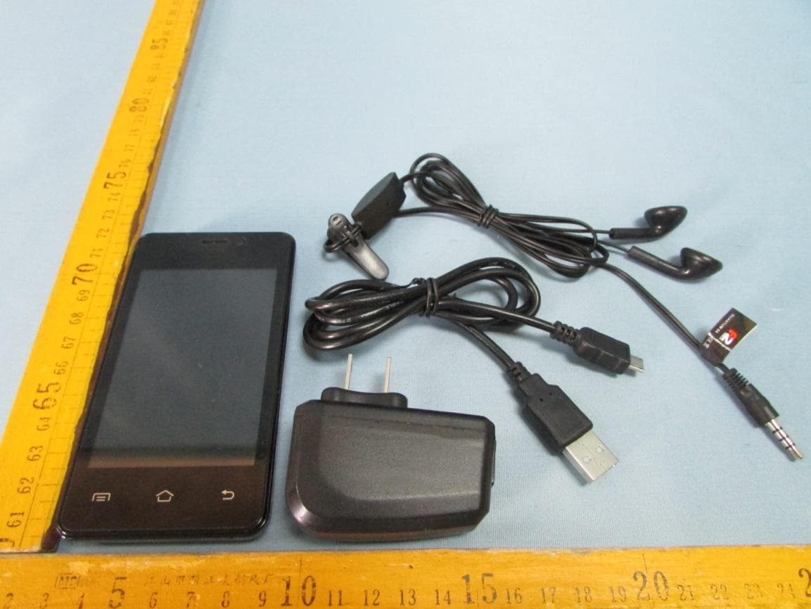
2ACEVAXF35
Aug 06, 20143.5 inch smartphone
Equipment Class
PCE - PCS Licensed Transmitter held to ear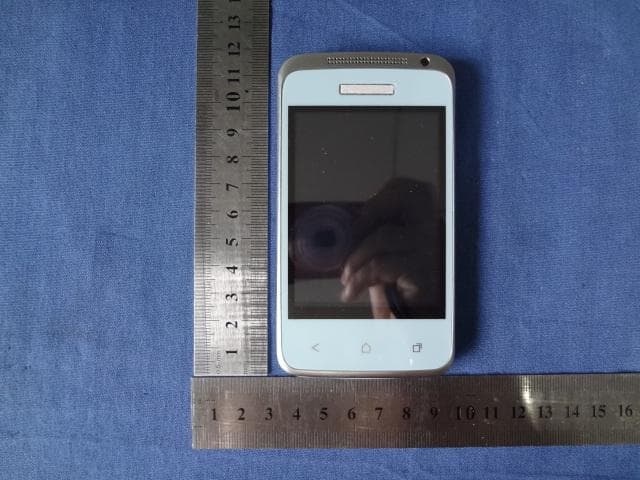
2ACEVF2BRIOF25
May 22, 2014Mobile phone
Equipment Class
DTS - Digital Transmission System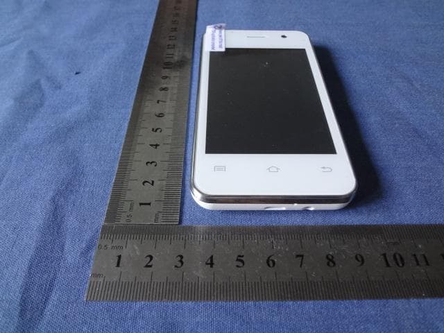
2ACEVF2NEOF30
May 19, 2014Mobile phone
Equipment Class
PCE - PCS Licensed Transmitter held to ear