2AFGR-APS2652DZigbee module
Altenergy Power System Inc.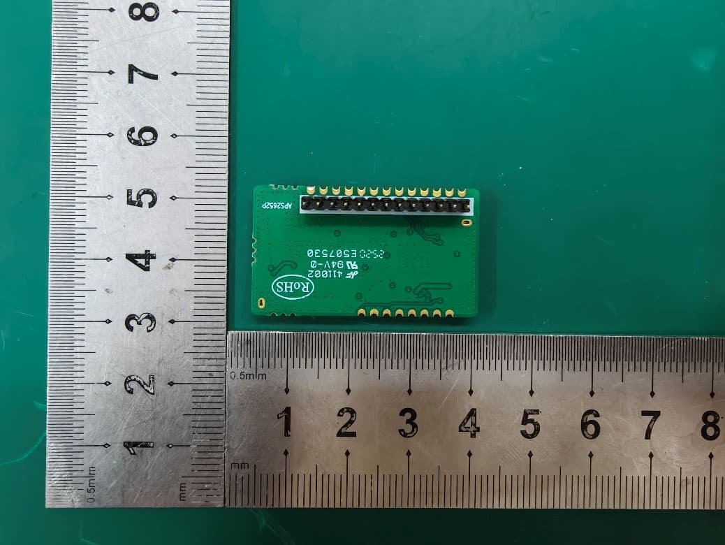
Click to zoom
Application Details
- Equipment Class
- DTS - Digital Transmission System
- Date of Grant
- Sep 30, 2025
- Application Purpose
- Original Equipment
- Equipment Note
- Zigbee module
- Frequency Range
- 2405.00000000 - 2480.00000000
- Company
- Altenergy Power System Inc.
- Country
- China
Documents & Files
Document Text
Text extracted from the exhibit documents filed with the FCC. Open a document above to read the original.
Users Manual
Company Name:Altenergy Power System Inc. Address:Building 2, No. 522, Yatai Road, Jiaxing, China 314050 User Manual for APS2652D User Manual for APS2652D The model used ZigBee PRO protocol to send RF signals for device communication. The model can be used after pairing with a dedicated device which was installed with a receiver dongle. APS2652D was used as a dongle which need to be installed in customer’s device. It offers UART to communicate with customer’s device according predefined protocol. 1:product figure 2:Technical specifications RF operating frequency: 2405MHz ~ 2480MHz Channel spacing: 5MHz Channel wide:2MHz Modulation method: OQPSK Communication rate: 250Kbps Average operating current: <20mA Operating voltage:2V-3.6V Max receiving distance:>100M Normal operating receiving distance: 100M 3. Pin Descriptions Pin name Pin type Description DIO12 Digital I/O GPIO DIO13 Digital I/O GPIO DIO23 Digital or Analog I/O GPIO analog capability DIO24 Digital or Analog I/O GPIO analog capability DIO25 Digital or Analog I/O GPIO analog capability DIO26 Digital or Analog I/O GPIO analog capability DIO27 Digital or Analog I/O GPIO analog capability JTAG_TMS Digital I/O JTAG TMS, high-drive capability JTAG_TCK Digital JTAG TCK VDD Power 2V–3.6-V digital power-supply connection GND Ground Connect to GND RESET_N Digital input Reset, active-low 4. Package Size 5.Caution FCC: Any Changes or modifications not ex press ly approved by the party responsible for compliance could void the user’s authority to operate the equipment. This device co mplies with part 15 of the FCC Rules. Operation is subject to the following two conditions: (1)This device may not cause harmful interference, and (2)This device must accept any interference received, including interference that may cause undesired operation. Note: This equipment has been tested and found to comply with the limits for a Class B digital device, pursuant to part 15 of the FCC Rules. T hese limits are designed to provide reasonable protection against harmful interference in a residential installation. This equipment generates, uses and can radiate radio frequency energy and, if not installed and used in accordance with the instructions, may cause harmful interference to radio communications. However, there is no guarantee that int erference will not occur in a particular installation. If this equipment does cause harmful interference to radio or television reception, which can be determined by turning the equipment off and on, the user is encouraged to try to correct the interference by one or more of the following measures: —Reori ent or relocate the receiving antenna. —Increase the separation between the equipment and receiver. —Connect the equ ipment into an outlet on a circuit different from that to which the receiver is connected. —Consult the dealer or an experienced radio/TV technician for help. RF Exposure Statement This equipment com plies with FCC radiation exposure limits set forth for an uncontrolled environment. This equipment should be installed and operated with minimum distance 20cm between the radiator and your body. FCC Label Instructions If using a permanently affixed label, the modular transmitter must be labeled with its own FCC identification number, and, if the FCC identification number is not visible when the module is installed inside another device, then the outside of the device into which the module is installed must also display a label referring to the enclosed module. This exterior label can use wording such as the following: “Contains FCC ID:2AFGR-APS2652D”. Any similar wording that expresses the same meaning may be used. The Grantee may either provide such a label, an example of which must be included in the application for equipment authorization, or, must provide adequate instructions along with the module which explain this requirement. OEM Guidance •Applicable FCC rules This device complies with part 15.247 of the FCC Rules. •The specific operational use conditions This module can be used in IoT devices. The input voltage to the module is nominally 3.3 V DC. The operational ambient temperature of the module is -40 °C ~ 105 °C. the external antenna is allowed, s uch as Monopole antenna. •Limited module procedures N/A •Trace antenna designs N/A •RF exposure considerations The equipment complies with FCC radiation exposure limits set forth for an uncontrolled environment. This equipment should be installed and operated with minimum distance 20cm between the radiator and your body. If the equipment built into a host as a portable usage, the additional RF exposure evaluation may be required as specified by 2.1093. •Antennas Antenna type: Monopole Antenna; Peak antenna gain : 3.26 dBi •Label and compliance information An exterior label on OEM’s end product can use wording such as the following: “Contains Transmitter Module FCC ID: 2AFGR-APS2652D” or “Contains FCC ID: 2AFGR-APS2652D” •Information on test modes and additional testing requirements The modular transmitter has been fully tested by the module grantee on the required number of channels,modulation types, and modes, it should not be necessary for the host installer to re-test all the available transmitter modes or settings. It is recommended that the host product manufacturer, installing the modular transmitter,perform some investigative measurements to confirm that the resulting composite system does not exceed the spurious emissions limits or band edge limits (e.g., where a different antenna may be causing additional emissions). The testing should check for emissions that may occur due to the intermixing of emissions with the other transmitters, digital c ircuitry, or due to physical properties of the host product (enclosure). This investigation is especially important when integrating multiple modular transmitters where the certification is based on testing each of them in a stand-alone configuration. It is important to note that host product manufacturers s…
Text truncated - open the document above for the full version.
Attestation Statements
Company: Altenergy Power System Inc. Add: Building 2, No.522, Yatai Road,Jiaxing 314050 China Tel: +86-573-83986966 Fax: +86-573-83986966 E-mail: [email protected] Attestation Letter Date: 05/30/2025 FEDERAL COMMUNICATIONS COMMISSIONS Authorization and Evaluation Division 7435 Oakland Mills Road Columbia, MD 21046 Ref: Attestation Statements CFR 47 §2.911 (d) (5) (i) (ii) Filing FCC ID: 2AFGR-APS2652D Altenergy Power System Inc.(“the applicant”) certifies that the equipment for which authorization is sought is not “covered” equipment prohibited from receiving an equipment authorization pursuant to section 2.903 of the FCC rules. Altenergy Power System Inc.(“the applicant”) certifies that as of the date of the filing of the application, the applicant is not identified on the Covered List as an entity producing “covered” equipment. Altenergy Power System Inc.(“the applicant”) certifies that the equipment does not use Kaspersky's software information. Sincerely, Signature: Contact Person: Guofeng Jiang Title: Director
Attestation Statements
U.S. AGENT LETTER OF ATTESTATION Date: 2025-05-30 FEDERAL COMMUNICATIONS COMMISSION Authorization and Evaluation Division 7435 Oakland Mills Road Columbia, MD 21046 Ref: Attestation Statements CFR 47 §2.911(d)(7) Filing FCC ID: 2AFGR-APS2652D Altenergy Power System Inc.(“the Applicant”) certifies that, as of the date of the filing of the application, ALTENERGY POWER SYSTEMS USA INC. (U.S. agent). is our designated U.S. agent for service of process for the above referenced FCC ID. Altenergy Power System Inc. (“the Applicant”) accepts to maintain an agent for no less than one year after the grantee has terminated all marketing and importation or the conclusion of any Commission-related proceeding involving the equipment. ALTENERGY POWER SYSTEMS USA INC. (U.S. agent). accepts, as of the date of the filing of the application, the obligation of the designated U.S. agent for service of process for the above referenced FCC ID. Designated U.S. Agent Information: Company Name: ALTENERGY POWER SYSTEMS USA INC. Address: 600 Ericksen Ave NE, STE 200,Bainbridge IS, WA 98110-2875 United States FRN: 0034051862 Tel.: (57) 383-98818 Email: [email protected] Signed by (printed name): Guofeng Jiang Signature: Applicant: Altenergy Power System Inc. Add:Building 2, No.522, Yatai Road,Jiaxing 314050 China FRN: 0024770307 Tel: +86-573-83986966 Email: [email protected] Signed by (printed name): Guofen Jiang Signature:
Cover Letter(s)
Company name: Altenergy Power System Inc. Address: Building 2, No.522, Yatai Road,Jiaxing 314050 China Tel: +86-573-83986966 Fax: +86-573-83986966 Email: [email protected] FCC Authorization Date:2025-05-30 FEDERAL COMMUNICATIONS COMMISSION Authorization and Evaluation Division 7435 Oakland Mills Road Columbia, MD 21046 Subject: Agent Authorization To whom it may concern: We, Altenergy Power System Inc., hereby authorizes Bay Area Compliance Laboratories Corp. (Kunshan) to act on its behalf in all matters relating to application for Equipment authorization, including the signing of all documents relating to these matters. All acts carried out by Bay Area Compliance Laboratories Corp. (Kunshan) on our behalf shall have the same effect as our own action. We, the undersigned, hereby certify that we are not subject to a denial of federal benefits, that includes FCC benefits, pursuant to Section 5301 of the Anti-Drug Abuse Act of 1988, 21 U.S.C. 862. This authorization is valid until further written notice from the applicant. Sincerely Yours, Signature: Printed Name: Guofeng Jiang Title: Director QA-FR-170-B
Cover Letter(s)
QA-FR-171-A Company name: Altenergy Power System Inc. Address: Building 2, No.522, Yatai Road,Jiaxing 314050 China Tel: +86-573-83986966 Fax: +86-573-83986966 Email: [email protected] FCC Confidential Authorization Date:2025-05-30 FEDERAL COMMUNICATIONS COMMISSIONS Authorization and Evaluation Division 7435 Oakland Mills Road Columbia, MD 21046 Subject: Confidentiality Request regarding application for certification of FCC ID: 2AFGR-APS2652D In accordance with Sections 0.457 and 0.459 of the Commission’s Rules, Altenergy Power System Inc. hereby requests long-term confidential treatment of information accompanying this application as outlined below: Block Diagram Schematics Operation Description The above materials contain proprietary and confidential information not customarily released to the public. The public disclosure of these materials provides unjustified benefits to its competitors in the market. Sincerely, Signature: Printed Name: Guofeng Jiang Title: Director
Cover Letter(s)
Company: Altenergy Power System Inc. Add: Building 2, No.522, Yatai Road,Jiaxing 314050 China Tel: +86-573-83986966 Fax: +86-573-83986966 E-mail: [email protected] Applicant Altenergy Power System Inc. FCC ID: 2AFGR‐APS2652D Section 15.212 Modular Transmitters Request for Modular Approval Request for Limited Modular Approval Requirements EUT Conditions Comply(Y/N) Single Modular Approval Requirements 1 The radio elements of the modular transmitter must have their own shielding. The physical crystal and tuning capacitors may be located external to the shielded radio elements. Refer to external photos. This module does have shield cover. Y 2 The modular transmitter must have buffered modulation/data inputs (if such inputs are provided) to ensure that the module will comply with part 15 requirements under conditions of excessive data rates or over‐modulation. All inputs to the modules are buffered through logic or microprocessor inputs. Refer to Schematics. Y 3 The modular transmitter must have its own power supply regulation. The Module uses the chip CC2652P7 with built‐in power management components, the module rated power is 3.3V power, Refer to schematics. Y 4 The modular transmitter must comply with the antenna and transmission system requirements of §§15.203, 15.204(b) and 15.204(c). The antenna must either be permanently attached or employ a “unique” antenna coupler (at all connections between the module and the antenna, including the cable). The “professional installation” provision of §15.203 is not applicable to modules but can apply to limited modular approvals under paragraph (b) of this section. The modular transmitter has a monopole antenna arrangement for 2.4G Zigbee, Refer to EUT photo. Y 5 The modular transmitter must be tested in a stand‐alone configuration, i.e., the module must not be inside another device during testing for compliance with part 15 requirements. Unless the transmitter module will be battery powered, it must comply with the AC line conducted requirements found in §15.207. AC or DC power lines and data input/output lines connected to the module must not contain ferrites, unless they will be marketed with the module (see §15.27(a)). The length of these lines shall be the length typical of actual use or, if that length is unknown, at least 10 centimeters to insure that there is no coupling between the case of the module and supporting equipment. Any accessories, peripherals, or support equipment connected to the module during testing shall be unmodified and commercially available (see §15.31(i)). The modular transmitter is connected to the controlled board when testing. Please refer to setup photo. Y 6 If using a permanently affixed label, the modular transmitter must be labeled with its own FCC identification number, and, if the FCC identification number is not visible when the module is installed inside another device, then the outside of the device into which the module is installed must also display a label referring to the enclosed module. This exterior label can use wording such as the following:“ContainsTransmitter Module FCC ID: 2AFGR‐APS2652D” Any similar wording that expresses the same meaning may be used. The Grantee may either provide such a label, an example of which must be included Refer to the label.Y in the application for equipment authorization, or, must provide adequate instructions along with the module which explain this requirement. In the latter case, a copy of these instructions must be included in the application for equipment authorization. 7 The modular transmitter must comply with any specific rules or operating requirements that ordinarily apply to a complete transmitter and the manufacturer must provide adequate instructions along with the module to explain any such requirements. A copy of these instructions must be included in the application for equipment authorization. Refer to manual Y 8 The modular transmitter must comply with any applicable RF exposure requirements in its final configuration. The EUT comply with RF exposure requirements § 2.1091.If the device built into a host as a portable usage, the RF exposure evaluation may be required as specified by § 2.1093. Y Sincerely Yours, Signature: Printed Name: Guofeng Jiang Title: Director
External Photos
Bay Area Compliance Laboratories Corp. (Kunshan) Project No.: RSHA250530004 1 / 2 EXHIBIT A - EUT EXTERNAL PHOTOGRAPHS Bay Area Compliance Laboratories Corp. (Kunshan) Project No.: RSHA250530004 2 / 2 Antenna
ID Label/Location Info
』 36 Mode: APS2652D FCC ID: 2AFGR-APS2652D IC: 20481-APS2652D 勹 20.5 NOTES 1) SHIELDING COVER SURFACE SMOOTH , NO SCRATCH , DEFORMATION , DISTORTION AND OTHER ILLS 2) WHITE BACKGROUND LABEL SHOULD WITH CLEARLY BLACK FONTS
Internal Photos
Bay Area Compliance Laboratories Corp. (Kunshan) Project No.: RSHA250530004 1 / 1 EXHIBIT B - EUT INTERNAL PHOTOGRAPHS
RF Exposure Info
Bay Area Compliance Laboratories Corp. (Kunshan) Report No.: RSHA250530004-00A Page 14 of 45 FCC §1.1310 & §2.1091 –MAXIMUM PERMISSIBLE EXPOSURE (MPE) Applicable Standard According to subpart §2.1091 and subpart §1.1310, systems operating under the provisions of this section shall be operated in a manner that ensures that the public is not exposed to radio frequency energy level in excess of the Commission’s guidelines. Limits for Maximum Permissible Exposure (MPE) (§1.1310, §2.1091) (B) Limits for General Population/Uncontrolled Exposure Frequency Range (MHz) Electric Field Strength (V/m) Magnetic Field Strength (A/m) Power Density (mW/cm 2 ) Averaging Time (minutes) 0.3-1.34 614 1.63 *(100) 30 1.34-30 824/f 2.19/f *(180/f²) 30 30-300 27.5 0.073 0.2 30 300-1500 / / f/1500 30 1500-100,000 / / 1.0 30 f = frequency in MHz; * = Plane-wave equivalent power density; According to §1.1310 and §2.1091 RF exposure is calculated. Calculated Formulary Predication of MPE limit at a given distance S = PG/4πR² = power density (in appropriate units, e.g. mW/cm 2 ); P = power input to the antenna (in appropriate units, e.g., mW); G = power gain of the antenna in the direction of interest relative to an isotropic radiator, the power gain factor, is normally numeric gain; R = distance to the center of radiation of the antenna (appropriate units, e.g., cm); Calculated Data: Mode Frequency Range (MHz) Antenna Gain ★Tune-up Conducted Output Power Evaluation Distance (cm) Power Density (mW/cm 2 ) MPE Limit (mW/cm 2 ) (dBi) (numeric) (dBm) (mW) Zigbee 2405~2480 3.26 2.12 4.0 2.51 20 0.0011 1.0 Note: 1. For the above tune up power were declared by the manufacturer. Result: The device meet FCC MPE at 20 cm distance.
Test Report
Antenna name:3010-0221 Manufacturer:SHENZHEN KYD ELECTRONIC CO.,LTD 3rd Floor, Building 77, Xinsha Industrial City, Pinghu Street, Longgang District, Shenzhen, Guangdong Province Frequency ID123456789101112131415161718192021 Frequency (MHz) 2400 .0 2405 .0 2410 .0 2415 .0 2420 .0 2425 .0 2430 .0 2435 .0 2440 .0 2445 .0 2450 .0 2455 .0 2460 .0 2465 .0 2470 .0 2475 .0 2480 .0 2485 .0 2490 .0 2495 .0 2500 .0 Efficiency (d Bi) -3.10-3.16-3.03-2.98-2.94-2.78-2.87-2.81-2.82-1.93-1.92-1.91-1.97-1.92-1.88-1.83-1.72-1.61-1.59-1.52-1.55 Gain (dBi ) 2.652.502.582.582.582.662.472.442.403.263.183.042.822.772.842.963.083.153.133.213.16 Efficiency (% ) 48.9348.3549.8350.4050.8152.7451.5852.3352.2364.1264.2864.3763.4764.2064.8665.5667.2468.9669.2970.5370.00 Directivity (dB)5.765.665.605.565.525.445.355.255.225.195.094.964.804.694.724.794.804.764.724.734.71 Peak Gain P osition (Theta) 135.00135.00135.00135.00135.00135.00135.00135.00135.00135.00135.00135.00135.00135.00150.00150.00150.00150.00150.00150.00150.00 Peak Gain P osition (Phi) 225.00225.00225.00225.00225.00225.00225.00225.00225.00225.00225.00240.00240.00240.00225.00225.00225.00225.00225.00225.00225.00 Efficiency ThetaPol (%)31.8132.2033.5634.0234.1135.8135.6136.6636.3544.3444.7845.6645.9546.7847.0447.3649.2351.4252.2052.9352.38 Efficiency Phi Pol (%) 17.1216.1616.2616.3816.7016.9315.9715.6715.8819.7819.4918.7117.5217.4217.8318.2018.0017.5417.0917.6017.62 Upper Hem. Efficiency (%) 19.9019.7820.5220.9621.2922.2922.0822.6222.6627.8828.0028.0727.7228.0828.4228.7529.6230.6731.0831.7931.76 Lower Hem. Efficiency (%)29.0328.5829.3029.4329.5230.4529.5129.7129.5736.2436.2736.3035.7536.1336.4436.8137.6138.2938.2138.7438.25 VER7 T90(H)圆度6.176.126.056.005.975.955.945.945.925.965.975.975.995.985.815.695.595.505.465.385.33 Gain 15deg (dBi) E1(XZ)波瓣宽度18.0019.0020.0020.0019.0020.0020.0020.0020.0020.0020.0020.0035.0036.0037.0037.0038.0039.0039.0041.0041.00 E1(XZ)前后 比 0.000.000.000.000.000.000.000.000.000.000.000.000.040.230.240.260.450.690.810.690.61 E2(YZ)波瓣宽度30.0030.0032.0032.0033.0033.0034.0034.0035.0035.0035.0035.0035.0034.0035.0035.0035.0036.0036.0036.0037.00 E2(YZ)前后比4.935.045.015.045.095.145.215.245.185.095.135.255.335.395.445.555.635.675.735.785.77 最大 增益 处轴比(P)0.670.610.780.820.850.710.610.520.670.850.940.680.880.874.924.754.494.434.584.754.67 顶点(Theta=0)处轴比(P)11.5311.3710.9410.6510.7610.9010.7510.329.859.669.779.969.919.749.9910.7612.1313.6414.7215.9117.37 仰角10度最 差 (大)轴比(P)85.8363.6270.1360.5358.3284.5864.3755.4465.9152.4652.2252.2745.0452.0656.2756.2750.4450.7354.5356.1055.81 Hc(XY)波瓣宽度101.00100.00100.0099.0099.0099.0099.00100.00100.00101.00102.00101.00102.00102.00103.00104.00104.00104.00104.00105.00105.00 Hc(XY)前后 比 0.710.941.131.171.141.201.251.261.171.061.061.101.251.301.231.191.301.461.521.451.41 左旋圆极化效率(%)24.8924.6725.4725.8026.0527.0626.5127.0026.9133.0833.0332.8332.1832.6233.0433.4034.1934.9935.1035.6335.44 右旋圆极化效率(%)24.0423.6924.3624.5924.7525.6825.0825.3325.3131.0431.2431.5431.2931.5831.8232.1633.0433.9634.1934.9034.56 Empty max70.53 min48.35 48.35 70 .53 0.00 10.00 20.00 30.00 40.00 50.00 60.00 70.00 80.00 90.00 100.00 2400.02405.02410.02415.02420.02425.02430.02435.02440.02445.02450.02455.02460.02465.02470.02475.02480.02485.02490.02495.02500.0 Efficiency (%) Max-Mi n 3.26 2.40 -4.00 -3 .00 -2.00 -1.00 0.00 1.00 2.00 3.00 4.00 2400.02405.02410.02415.02420.02425.02430.02435.02440.02445.02450.02455.02460.02465.02470.02475.02480.02485.02490.02495.02500.0 0.00 1 0.00 20.00 30.00 40.00 50.00 60.00 70.00 80.00 90.00 100.00 2400.02405.02410.02415.02420.02425.02430.02435.02440.02445.02450.02455.02460.02465.02470.02475.02480.02485.02490.02495.02500.0 Efficie ncy ThetaPol (%) Efficie ncy PhiPol (%) ANTENN A TECHNOLOGY 2400.0MHz H+V, Eff: 48.9%Back View2400.0MHz Total(E1-XZ), Max= 0.65dBi2400.0MHz Total(E2-YZ), Max= 1.79dBiTotal(H-XY), Max= -0.38dBi, CirD=6.172400.0MHz Hpol, Eff: 31.8%2400.0MHz Hpol(E1-XZ), Max= -0.84dBi2400.0MHz Hpol(E2-YZ), Max= 0.89dBiHpol(H-XY), Max= -0.52dBi, CirD=6.482400.0MHz Vpol, Eff: 17.1%2400.0MHz Vpol(E1-XZ), Max= 0.58dBi2400.0MHz Vpol(E2-YZ), Max= -3.82dBiVpol(H-XY), Max= -3.79dBi, CirD=26.22 2.65 0.81 -1.03 -2.87 -4.71 -6.56 -8.4 -10.24 -12.08 -13.92 -15.77 -17.61 -19.45 -21.29 -23.14 -24.98 -26.82 -28.66 2405.0MHz H+V, Eff: 48.4%Back View2405.0MHz Total(E1-XZ), Max= 0.36dBi2405.0MHz Total(E2-YZ), Max= 1.70dBiTotal(H-XY), Max= -0.34dBi, CirD=6.122405.0MHz Hpol, Eff: 32.2%2405.0MHz Hpol(E1-XZ), Max= -0.78dBi2405.0MHz Hpol(E2-YZ), Max= 0.85dBiHpol(H-XY), Max= -0.48dBi, CirD=6.362405.0MHz Vpol, Eff: 16.2%2405.0MHz Vpol(E1-XZ), Max= 0.29dBi2405.0MHz Vpol(E2-YZ), Max= -3.95dBiVpol(H-XY), Max= -4.11dBi, CirD=24.12 2.5 0.66 -1.18 -3.03 -4.87 -6.71 -8.55 -10.39 -12.24 -14.08 -15.92 -17.76 -19.6 -21.45 -23.29 -25.13 -26.97 -28.82 2410.0MHz H+V, Eff: 49.8%Back View2410.0MHz Total(E1-XZ), Max= 0.35dBi2410.0MHz Total(E2-YZ), Max= 1.75dBiTotal(H-XY), Max= -0.17dBi, CirD=6.052410.0MHz Hpol, Eff: 33.6%2410.0MHz Hpol(E1-XZ), Max= -0.59dBi2410.0MHz Hpol(E2-YZ), Max= 0.91dBiHpol(H-XY), Max= -0.31dBi, CirD=6.242410.0MHz Vpol, Eff: 16.3%2410.0MHz Vpol(E1-XZ), Max= 0.29dBi2410.0MHz Vpol(E2-YZ), Max= -3.78dBiVpol(H-XY), Max= -4.23dBi, CirD=23.79 2.58 0.73 -1.11 -2.95 -4.79 -6.63 -8.48 -10.32 -12.16 -14 -15.84 -17.69 -19.53 -21.37 -23.21 -25.05 -26.9 -28.74 2415.0MHz H+V, Eff: 50.4%Back View2415.0MHz Total(E1-XZ), Max= 0.39dBi2415.0MHz Total(E2-YZ), Max= 1.68dBiTotal(H-XY), Max= -0.16dBi, CirD=6.002415.0MHz Hpol, Eff: 34.0%2415.0MHz Hpol(E1-XZ), Max= -0.55dBi2415.0MHz Hpol(E2-YZ), Max= 0.84dBiHpol(H-XY), Max= -0.31dBi, CirD=6.162415.0MHz Vpol, Eff: 16.4%2415.0MHz Vpol(E1-XZ), Max= 0.34dBi2415.0MHz Vpol(E2-YZ), Max= -3.64dBiVpol(H-XY), Max= -4.28dBi, CirD=23.61 2.58 0.74 -1.1 -2.94 -4.79 -6.63 -8.47 -10.31 -12.15 -14 -15.84 -17.68 -19.52 -21.36 -23.21 -25.05 -26.89 -28.73 2420.0MHz H+V, Eff: 50.8%Back View2420.0MHz Total(E1-XZ), Max= 0.48dBi2420.0MHz Total(E2-YZ), Max= 1.59dBiTotal(H-XY), Max= -0.20dBi, CirD=5.972420.0MHz Hpol, Eff: 34.1%2420.0MHz H…
Text truncated - open the document above for the full version.
Test Report
Note: This test report is prepared for the customer shown above and for the device described herein. It may not be duplicated or used in part without prior written consent from Bay Area Compliance Laboratories Corp. (Kunshan). This report must not be used by the customer to claim product certification, approval, or endorsement by NVLAP, or any agency of the U.S. Government. FCC PART 15.247 TEST REPORT For Altenergy Power System Inc. Building 2, No. 522, Yatai Road, Jiaxing 314050 China FCC ID: 2AFGR-APS2652D R e p o r t T y p e : O r i gi n a l R e p o r t P r o d u c t N a m e: Zigbee module Report Number: RSHA250530004-00A Report Date: 2025-09-12 Reviewed By: Bard Liu Approved By: Kyle Xu Prepared By: Bay Area Compliance Laboratories Corp. (Kunshan) No.248 Chenghu Road, Kunshan, Jiangsu Province, China Tel: +86-512-86175000 Fax: +86-512-88934268 www.baclcorp.com.cn Bay Area Compliance Laboratories Corp. (Kunshan) Report No.: RSHA250530004-00A Page 2 of 45 TABLE OF CONTENTS REPORT REVISION HISTORY................................................................................................................................. 4 GENERAL INFORMATION ....................................................................................................................................... 5 PRODUCT DESCRIPTION FOR EQUIPMENT UNDER TEST (EUT) ..................................................................................... 5 OBJECTIVE ................................................................................................................................................................... 5 TEST METHODOLOGY .................................................................................................................................................. 5 MEASUREMENT UNCERTAINTY .................................................................................................................................... 6 TEST FACILITY ............................................................................................................................................................. 6 SYSTEM TEST CONFIGURATION .......................................................................................................................... 7 DESCRIPTION OF TEST CONFIGURATION ...................................................................................................................... 7 EUT EXERCISE SOFTWARE .......................................................................................................................................... 7 SPECIAL ACCESSORIES ................................................................................................................................................. 9 EQUIPMENT MODIFICATIONS ....................................................................................................................................... 9 SUPPORT EQUIPMENT LIST AND DETAILS .................................................................................................................... 9 EXTERNAL I/O CABLE.................................................................................................................................................. 9 BLOCK DIAGRAM OF TEST SETUP .............................................................................................................................. 10 TEST EQUIPMENT LIST ......................................................................................................................................... 12 SUMMARY OF TEST RESULTS ............................................................................................................................. 13 FCC §1.1310 & §2.1091 –MAXIMUM PERMISSIBLE EXPOSURE (MPE) ....................................................... 14 FCC §15.203 – ANTENNA REQUIREMENT .......................................................................................................... 15 APPLICABLE STANDARD ............................................................................................................................................ 15 ANTENNA CONNECTOR CONSTRUCTION .................................................................................................................... 15 FCC §15.207 (a) – AC LINE CONDUCTED EMISSIONS ..................................................................................... 16 APPLICABLE STANDARD ............................................................................................................................................ 16 TEST SYSTEM SETUP .................................................................................................................................................. 16 EMI TEST RECEIVER SETUP ....................................................................................................................................... 16 TEST PROCEDURE ...................................................................................................................................................... 17 TEST RESULTS SUMMARY .......................................................................................................................................... 17 TEST DATA: SEE APPENDIX ....................................................................................................................................... 17 FCC §15.209, §15.205 & §15.247(d) - SPURIOUS EMISSIONS............................................................................. 18 APPLICABLE STANDARD ............................................................................................................................................ 18 TEST SYSTEM SETUP .................................................................................................................................................. 18 EMI TEST RECEIVER SETUP ...................................................................................................…
Text truncated - open the document above for the full version.
Test Setup Photos
Bay Area Compliance Laboratories Corp. (Kunshan) Project No.: RSHA250530004 1 / 4 EXHIBIT C - TEST SETUP PHOTOGRAPHS Conducted Emissions - Front View Conducted Emissions - Left View Bay Area Compliance Laboratories Corp. (Kunshan) Project No.: RSHA250530004 2 / 4 Radiated Emissions-Ground-parallel View (Below 30 MHz) Radiated Emissions-Perpendicular View (Below 30 MHz) Bay Area Compliance Laboratories Corp. (Kunshan) Project No.: RSHA250530004 3 / 4 Radiated Emissions-Parallel View (Below 30 MHz) Radiated Spurious Emissions Test View (Below 1 GHz) Bay Area Compliance Laboratories Corp. (Kunshan) Project No.: RSHA250530004 4 / 4 Radiated Spurious Emissions Test View (1 GHz - 18 GHz ) Radiated Spurious Emissions Test View (18 GHz - 25 GHz)
Contact Information
Applicant
Guofeng Jiang(Director)
[email protected]Fax: 0573-83986966
Test Firm
Bay Area Compliance Laboratories Corp. (Kunshan)John Chan
Technical Specifications
| # | Rule Parts | Frequency Range | Power Output |
|---|---|---|---|
| 1 | 15C | 2.40 GHz - 2.48 GHz | 2.40 mW |
Other Applications from Altenergy Power System Inc.
2AFGR-APSC3
Apr 11, 2024Aps-c3
Equipment Class
DTS - Digital Transmission System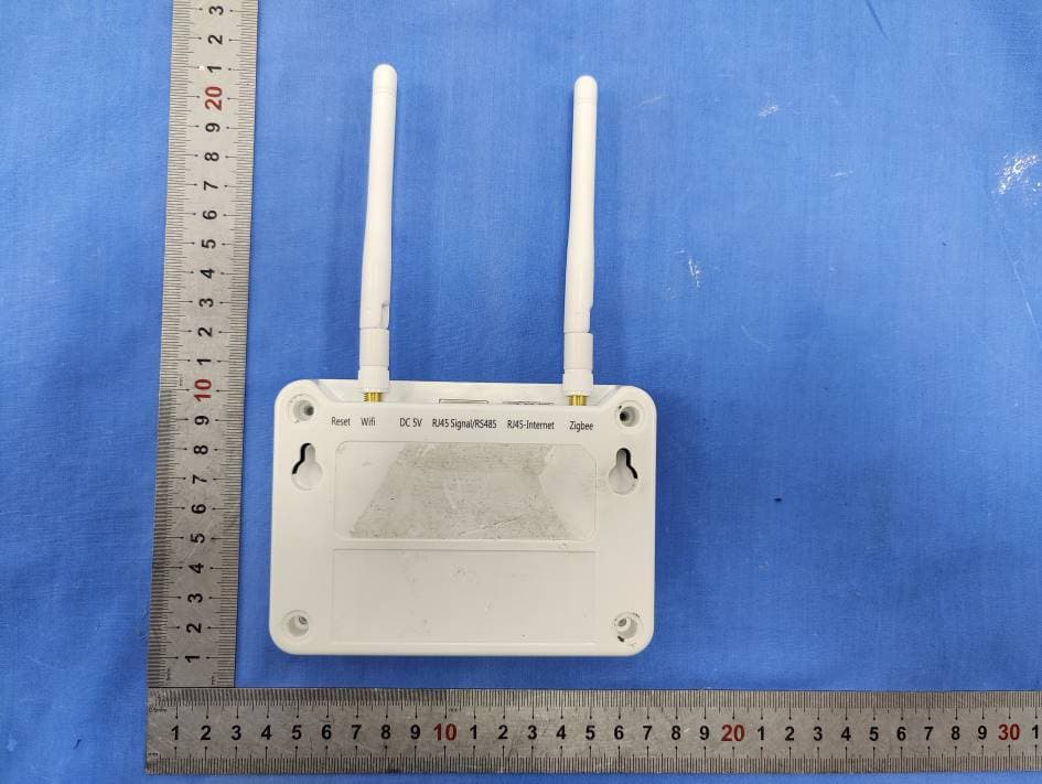
2AFGRECUR
Jan 25, 2021Energy Communication Unit
Equipment Class
DTS - Digital Transmission System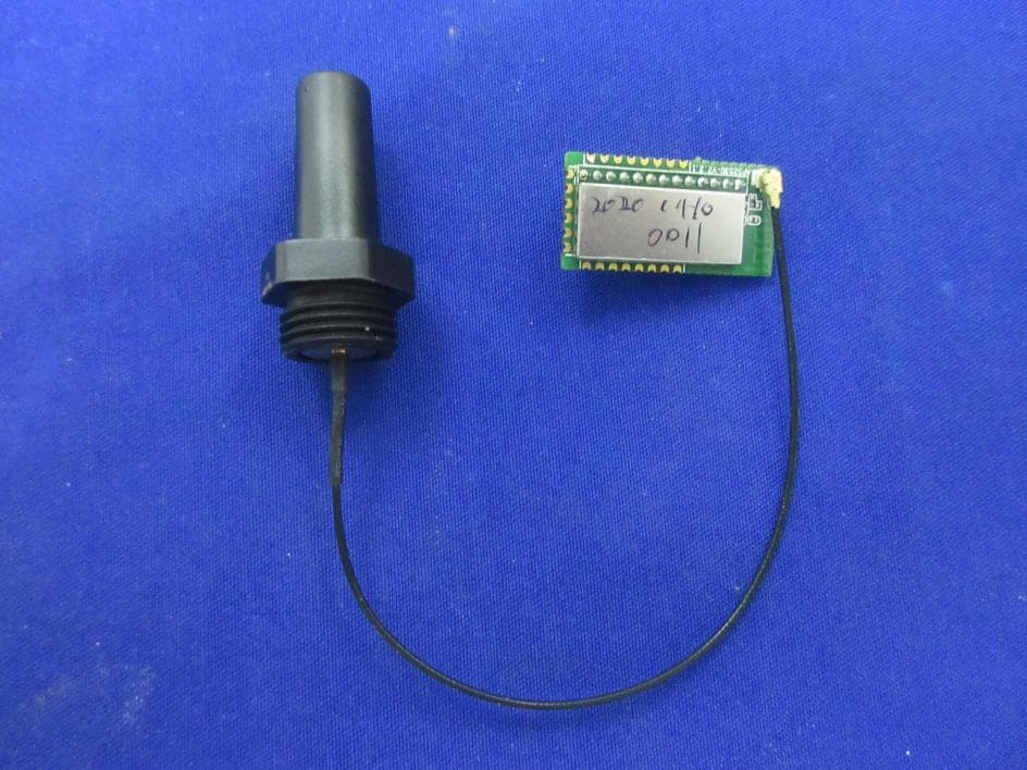
2AFGR-APS2530H
Jun 22, 2020Zigbee module
Equipment Class
DTS - Digital Transmission System
2AFGR-APS2530P
Sep 01, 2015ZigBee Module
Equipment Class
DTS - Digital Transmission System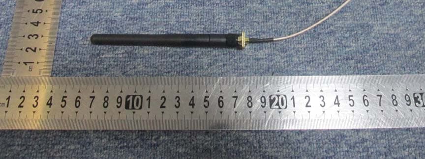
2AFGR-APS2530S
Sep 01, 2015ZigBee Module
Equipment Class
DTS - Digital Transmission System