2APA9-CMSXJ21EIMILAB C30
Shanghai Imilab Technology Co.,Ltd.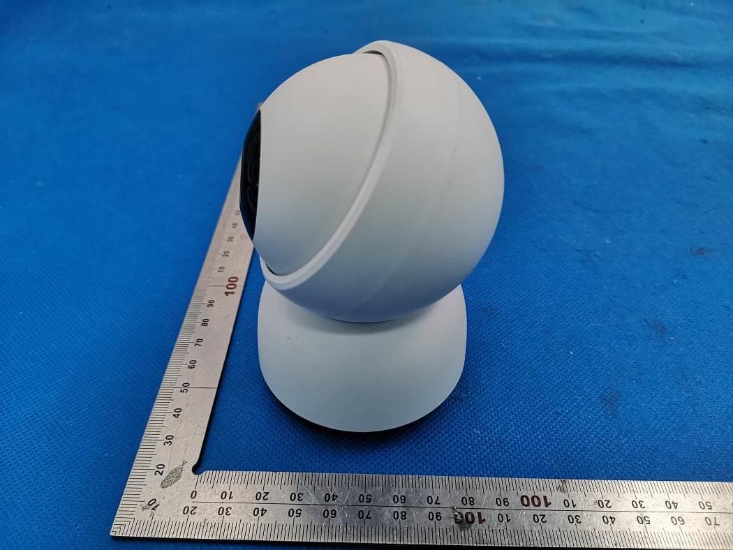
Click to zoom
Application Details
- Equipment Class
- NII - Unlicensed National Information Infrastructure TX
- Date of Grant
- Jan 21, 2021
- Application Purpose
- Original Equipment
- Date of Application
- Jan 21, 2021
- Equipment Note
- IMILAB C30
- Frequency Range
- 5745.00000000 - 5825.00000000
- Country
- China
Documents & Files
Document Text
Text extracted from the exhibit documents filed with the FCC. Open a document above to read the original.
Users Manual
V1.1 20201210 周晓玲 材质:太空梭105g无光铜亚粉 尺寸:80 75mm IPC021_E01 IMILAB C30CMSXJ21E 阿里巴巴普惠体 pantone cool Gray 11C Read this manual carefully before use, and retain it for future reference. IMILAB C30 Home Security Camera User Manual CONTENTS English01-09 10-18Deutsche 19-27Français 28-36Italiano 37-45Español 55-63Pусский 64-70Chinese 46-54Português Manufacturer: Shanghai Imilab Technology Co., Ltd. Address: Room 001A, Floor 11, Block 1, No. 588 Zixing Road, Minhang District, Shanghai, China For further information, please go to www.imilab.com. Support: [email protected] 英 修改内容版本 新建文档V1.0 修 改 记 录 Product Overview Package Contents: IMILAB C30 x 1, power cable x 1, wall mounting accessories pack x 1, user manual x 1 MicroSD Slot (Can be revealed by pushing the lens upward) Lens Status indicator Loudspeaker Micro-USB Charging port MIC Front View Rear View EN-01 Reset button IMILAB C30 can be placed on a number of horizontal surfaces, such as a writing desk, dining table, and coffee table. It can also be mounted on the wall. Mounted IMILAB C30 on a Wall: 1. Drill two holes on the wall by using the base of the IMILAB C30 as a template. It is recommended that you mark the locations of the hole with a pencil before drilling. The diameter of each hole is approximately 6 mm, and the depth is approximately 30 mm. 2. Insert the two plastic anchors into the holes on the wall. Installation EN-02 3. Make sure to position the base unit so that the arrow is pointing up. Secure the base unit in place by tightening the screws into the plastic anchors. 4. Matching the grooves on the bottom of the camera unit with the raised area on the base unit. Press down until the two surfaces are flush, then turn the camera unit in either direction to lock it in position. Warning: To avoid any damages or injuries, the device must be securely fastened to the floor/wall as specified in the installation instructions. When mounting the security camera on a wall: Please note that the wall must be able to support at least triple the product's total weight. EN-03 1. If the indicator light is flashing orange, that means the device is activated successfully. Else, please reset the device. 2. Once the IMILAB C30 is turned on, please do not attempt to rotate its head by force. If the camera position is incorrect, adjustments can be made through the app. Product Instructions Turning the Device On IMILAB C30 will automatically activate once the power cable is inserted into the Micro-USB charging port. EN-04 MicroSD Indicator Light Steady blue on: connected/device status is normal Flashing blue: network error Flashing orange rapidly: waiting for connection Flashing orange slowly: system upgrade in progress Installing a MicroSD Card Make sure that the power to IMILAB C30 is already disconnected. Adjust the camera lens upward until the MicroSD slot is revealed, then insert the MicroSD card into the slot (the side with contact points must be facing down). Note: Please turn off the IMILAB C30‘s power supply before inserting or removing the MicroSD card. Please use a genuine Micro SD card manufactured by a qualified supplier, with a reading/writing speed of no less than U1/Class 10. (Maximum support capacity is 64 GB) Restore Factory Settings Press and hold the Reset button more than 5s, then you can hear the “reset succeed” voice. Data stored on the MicroSD card is not deleted. EN-05 Specifications Name: IMILAB C30 Model: CMSXJ21E Net Weight: 289 g Lens Angle: 100° Power input: 5 V 2 A Wireless Connectivity: Wi-Fi IEEE 802.11a/b/g/n/ac2.4GHz/5GHz FCC ID: xxxxx-IMILAB-C30 Expandable Memory: MicroSD card (up to 64 GB) Dimensions: 112 mm x 76 mm x 76 mm Operating Temperature: -10 °C to 40 °C Compatible With: Android 5.0 or iOS 9.0 or above Resolution: 2560 x 1440 Precautions The operating temperature range for this camera is between -10°C and 40°C. Do not use the camera in environments with temperatures above or below the specified range. The camera is a precision electronic product. In order to ensure its normal operation, do not install the camera in environments with high humidity levels nor allow water to get into it. To improve the camera's performance, do not place its lens facing or next to a reflective surface, such as glass windows or white walls, as this will cause the image to appear overly bright in areas close to the camera and darker in areas further away, or cause the camera to produce white images. Make sure the camera is installed in an area with a strong Wi-Fi signal. Do not place the camera near the objects that may affect its Wi-Fi signal, such as metal objects, microwave ovens. Under normal use of condition, this equipment should be kept a separation distance of at least 20 cm between the antenna and the body of the user. EN-07 Changes or modifications not expressly approved by the party responsible for compliance could void the user's authority to operate the equipment. This device complies with Part 15 of the FCC Rules. Operation is subject to the following two conditions: (1) This device may not cause harmful interference, and (2) This device must accept any interference received, including interference that may cause undesired operation. Note: This equipment has been tested and found to comply with the limits for a Class B digital device, pursuant to Part 15 of the FCC Rules. These limits are designed to provide reasonable protection against harmful interference in a residential installation. This equipment generates, uses, and can radiate radio frequency energy, and if not installed and used in accordance with the instructions, may cause harmful interference to radio communications. However, there is no guarantee that interference will not occur in a particular installation. If this equipment does cause harmful interference to radio or television reception, which can be determined by turning the equipment off and on, the user is encouraged to try to correct the interference by one or more of the following measures: -Reorient …
Text truncated - open the document above for the full version.
Cover Letter(s)
FCC Software Configuration Control Declaration Rev1.1.docx Shanghai Imilab Technology Co., Ltd. FCC Software Configuration Control Declaration Date: January 14, 2021 Federal Communications Commission 7435 Oakland Mills Road Columbia, MD 21046 USA Attn: OET Dept. Product/ Model Number: IMILAB C30 / CMSXJ21E Regarding FCC Country Code Selection guidelines identified in KDB 594280 v02r01. “All applications for equipment authorization for transmitters that can have radio parameters, or other technical parameters, reported to the Commission set by software must have an attestation indicating that no third party will have software, or configuration control, to program the device out of compliance of the technical rules under which it has been certified.” We declare that no third party will have software, or configuration control, to program the device out of compliance of the technical rules under which it has been certified. Name: wang hesong Date: 2021-01-14 Signature of applicant
Cover Letter(s)
Shanghai Imilab Technology Co., Ltd. Agent Authorization Company: Shanghai Imilab Technology Co., Ltd. Address: Room 001A, Floor 11, Block 1, No. 588 Zixing Road, Minhang District, Shanghai, China Product Name: IMILAB C30 Model Number(s): CMSXJ21E Product Description: IMILAB C30 We authorize MiCOM Labs Inc., 575 Boulder Court, Pleasanton, California 94566, USA, to act on our behalf on all matters concerning the certification of above named equipment. We declare that MiCOM Labs Inc. is allowed to forward all information related to the approval and certification of equipment to the regulatory agencies as required and to discuss any issues concerning the approval application. Any and all acts carried out by MiCOM Labs on our behalf shall have the same effect as acts of our own. Signature: Date: 2021-01-14 Name: wang hesong Company: Shanghai Imilab Technology Co., Ltd.
Cover Letter(s)
Shanghai Imilab Technology Co., Ltd. Office of Engineering Technology Federal Communications Commission 7435 Oakland Mills Road Columbia, MD 21046 USA Date: 2021-01-06 Subject; Request for Confidentiality FCC ID: 2APA9-CMSXJ21E To Whom It May Concern, Pursuant to the provisions of the Commission’s rules Title 47 Sections §0.457 and §0.459, we are requesting the Commission to withhold the following attachment(s) as confidential documents from public disclosure indefinitely. These documents contain detailed system and equipment descriptions and are considered as proprietary information in operation of the equipment. The public disclosure of these documents might be harmful to our company and would give competitors an unfair advantage in the market. Schematic Diagram Block Diagram Parts List Operational Description Software Security Description In additional to above mentioned documents, in order to comply with the marketing regulations in Title 47 CFR §2.803 and the importation rules in Title 47 CFR §2.1204, while ensuring that business sensitive information remains confidential until the actual marketing of newly authorized devices, we request Short Term Confidentiality of the following attachment(s); External Photos Test Setup Photos Internal Photos User Manual For 45 days, pursuant to Public Notice DA 04-1705. OR For 180 days pursuant to KDB 726920 D01. It is our understanding that all measurement test reports, FCC ID label format and correspondence during the certification review process cannot be granted as confidential documents and this information will be available for public review once the grant of equipment authorization is issued. Sincerely Shanghai Imilab Technology Co., Ltd. Contact person: wang hesong
External Photos
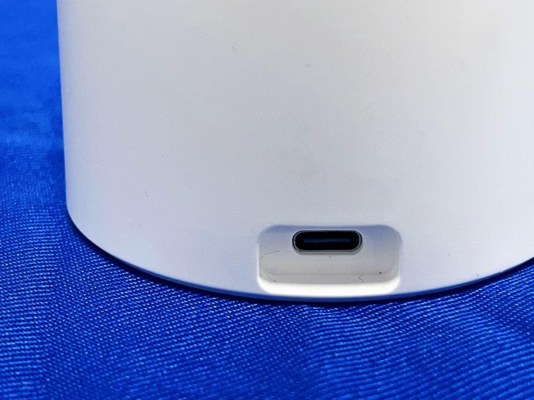
External Photos ALL VIEW OF EUT TOP VIEW OF EUT BOTTOM VIEW OF EUT FRONT VIEW OF EUT BACK VIEW OF EUT LEFT VIEW OF EUT RIGHT VIEW OF EUT VIEW OF EUT (PORT)-1 VIEW OF EUT (PORT)-2
External Photos
Page 1 of 14 EUT PHOTOS Report No.: AGC05877201202AP02 PRODUCT DESIGNATION : IMILAB C30 BRAND NAME : N/A MODEL NAME : CMSXJ21E APPLICANT : Shanghai Imilab Technology Co., Ltd. DATE OF ISSUE : Jan. 05, 2021 REPORT VERSION V1.0 Attestation of Global Compliance (Shenzhen) Co., Ltd Report No.: AGC05877201202AP02 Page 2 of 14 PHOTOGRAPHS OF EUT ALL VIEW OF EUT TOP VIEW OF EUT Report No.: AGC05877201202AP02 Page 3 of 14 BOTTOM VIEW OF EUT FRONT VIEW OF EUT Report No.: AGC05877201202AP02 Page 4 of 14 BACK VIEW OF EUT LEFT VIEW OF EUT Report No.: AGC05877201202AP02 Page 5 of 14 RIGHT VIEW OF EUT VIEW OF EUT (PORT)-1 Report No.: AGC05877201202AP02 Page 6 of 14 VIEW OF EUT (PORT)-2 OPEN VIEW OF EUT Report No.: AGC05877201202AP02 Page 7 of 14 INTERNAL VIEW-1 OF EUT INTERNAL VIEW-2 OF EUT Report No.: AGC05877201202AP02 Page 8 of 14 INTERNAL VIEW-3 OF EUT INTERNAL VIEW-4 OF EUT Report No.: AGC05877201202AP02 Page 9 of 14 INTERNAL VIEW-5 OF EUT INTERNAL VIEW-6 OF EUT Report No.: AGC05877201202AP02 Page 10 of 14 INTERNAL VIEW-7 OF EUT INTERNAL VIEW-8 OF EUT Report No.: AGC05877201202AP02 Page 11 of 14 INTERNAL VIEW-9 OF EUT INTERNAL VIEW-10 OF EUT Report No.: AGC05877201202AP02 Page 12 of 14 INTERNAL VIEW-11 OF EUT INTERNAL VIEW-12 OF EUT Report No.: AGC05877201202AP02 Page 13 of 14 INTERNAL VIEW-13 OF EUT INTERNAL VIEW-14 OF EUT Antenna Report No.: AGC05877201202AP02 Page 14 of 14 INTERNAL VIEW-15 OF EUT VIEW OF ADAPTER ----END OF REPORT---- Conditions of Issuance of Test Reports 1. All samples and goods are accepted by the Attestation of Global Compliance (Shenzhen) Co., Ltd (the “Company”) solely for testing and reporting in accordance with the following terms and conditions. The company provides its services on the basis that such terms and conditions constitute express agreement between the company and any person, firm or company requesting its services (the “Clients”). 2. Any report issued by Company as a result of this application for testing services (the “Report”) shall be issued in confidence to the Clients and the Report will be strictly treated as such by the Company. It may not be reproduced either in its entirety or in part and it may not be used for advertising or other unauthorized purposes without the written consent of the Company. The Clients to whom the Report is issued may, however, show or send it, or a certified copy thereof prepared by the Company to its customer, supplier or other persons directly concerned. The Company will not, without the consent of the Clients, enter into any discussion or correspondence with any third party concerning the contents of the Report, unless required by the relevant governmental authorities, laws or court orders. 3.The Company shall not be called or be liable to be called to give evidence or testimony on the Report in a court of law without its prior written consent, unless required by the relevant governmental authorities, laws or court orders. 4. The non-CMA report issued by AGC is only permitted to be used by the client as internal reference use and shall not be used for public demonstration purpose. 5. In the event of the improper use of the report as determined by the Company, the Company reserves the right to withdraw it, and to adopt any other additional remedies which may be appropriate. 6. Samples submitted for testing are accepted on the understanding that the Report issued cannot form the basis of, or be the instrument for, any legal action against the Company. 7. The Company will not be liable for or accept responsibility for any loss or damage however arising from the use of information contained in any of its Reports or in any communication whatsoever about its said tests or investigations. 8.Clients wishing to use the Report in court proceedings or arbitration shall inform the Company to that effect prior to submitting the sample for testing. 9. The Company is not responsible for recalling the electronic version of the original report when any revision is made to them. The Client assumes the responsibility to providing the revised version to any interested party who uses them. 10. Subject to the variable length of retention time for test data and report stored hereinto as otherwise specifically required by individual accreditation authorities, the Company will only keep the supporting test data and information of the test report for a period of six years. The data and information will be disposed of after the aforementioned retention period has elapsed. Under no circumstances shall we provide any data and information which has been disposed of after retention period. Under no circumstances shall we be liable for damage of any kind, including (but not limited to) compensatory damages, lost profits, lost data, or any form of special, incidental, indirect, consequential or punitive damages of any kind, whether based on breach of contract of warranty, tort (including negligence), product liability or otherwise, even if we are informed in advance of the possibility of such damages.
ID Label/Location Info
FCC ID Label Location FCC ID: 2APA9-CMSXJ21E
Internal Photos
Internal Photos OPEN VIEW OF EUT INTERNAL VIEW-1 OF EUT INTERNAL VIEW-2 OF EUT INTERNAL VIEW-3 OF EUT INTERNAL VIEW-4 OF EUT INTERNAL VIEW-5 OF EUT INTERNAL VIEW-6 OF EUT INTERNAL VIEW-7 OF EUT INTERNAL VIEW-8 OF EUT INTERNAL VIEW-9 OF EUT INTERNAL VIEW-10 OF EUT INTERNAL VIEW-11 OF EUT INTERNAL VIEW-12 OF EUT INTERNAL VIEW-13 OF EUT INTERNAL VIEW-14 OF EUT INTERNAL VIEW-15 OF EUT Antenna
RF Exposure Info
RF EXPOSURE EVALUATION 1. PRODUCT INFORMATION Product Description IMILAB C30 Model Name CMSXJ21E FCC ID 2APA9-CMSXJ21E 2. EVALUATION METHOD AND LIMIT Human exposure to RF emissions from mobile devices (47 CFR §2.1091) may be evaluated based on the MPE limits adopted by the FCC for electric and magnetic field strength and/or power density, as appropriate, since exposures are assumed to occur at distances of 20 cm or more from persons. LIMITS FOR GENERAL POPULATION / UNCONTROLLED EXPOSURE Frequency Range (MHz) E-field Strength (E) (V/m) Magnetic Field Strength (H) (A/m) Power Density (S) (mW/cm 2 ) Averaging Time |E| 2 , |H| 2 or S (Minutes) 0.3 -- 1.34 614 1.63 (100)* 30 1.34 -- 30 824/f 2.19/f (180/f 2 )* 30 30 -- 300 27.5 0.073 0.2 30 300 -- 1500 -- -- f/1500 30 1500 -- 100,000 -- -- 1.0 30 *Note: 1. f= Frequency in MHz * Plane-wave Equivalent Power Density 2. The averaging time for General Population/Uncontrolled exposure to fixed transmitters is not applicable for mobile and portable transmitters. See 47 CFR §§2.1091 and 2.1093 on source-based time-averaging requirement for mobile and portable transmitters. S=PG/4πR² Where: S=power density P=power input to antenna G=power gain of the antenna in the direction of interest relative to an isotropic radiator R=distance to the center of radiation of the antenna CALCULATION A minimum test separation distance ≥ 20 cm is required between the antenna and radiating structures of the device and nearby persons to apply mobile device exposure limits. The distance must be at least 20 cm and fully supported by the operating and installation configurations of the transmitter and its antenna(s), according to the source-based time-averaged maximum power requirements of § 2.1091(d)(2). In cases where cable losses or other attenuations are applied to determine compliance, the most conservative operating configurations and exposure conditions must be evaluated. 2.4G WIFI Antenna Gain=1.54dBi (Numeric 1.43), π=3.14 5G WIFI Antenna Gain=1.41dBi (Numeric 1.38), π=3.14 Note: 1. Only the worst case recorded. 2. The 2.4GHz WIFI band and 5GHz band can transmit simultaneously: 0.0085/1+0.0081/1=0.0166<1 3. conclusion Compliance the RF exposure requirement Frequency Output Power Output Power Power Density Power Density Limit MHz dBm mW mW/cm 2 mW/cm 2 2437 14.73 29.72 0.0085 1 Frequency Output Power Output Power Power Density Power Density Limit MHz dBm mW mW/cm 2 mW/cm 2 5310 14.84 29.79 0.0081 1
Test Report
Page 1 of 172 Report No.: AGC05877201202FE06 FCC ID : 2APA9-CMSXJ21E APPLICATION PURPOSE : Original Equipment PRODUCT DESIGNATION : IMILAB C30 BRAND NAME : N/A MODEL NAME : CMSXJ21E APPLICANT : Shanghai Imilab Technology Co., Ltd. DATE OF ISSUE : Jan. 05, 2021 STANDARD(S) TEST PROCEDURE(S) : FCC Part 15.407 KDB 789033 D02 v02r01 REPORT VERSION : V1.0 Attestation of Global Compliance (Shenzhen) Co., Ltd FCC Test Report Report No.: AGC05877201202FE06 Page 2 of 172 REPORT REVISE RECORD Report Version Revise Time Issued Date Valid Version Notes V1.0 / Jan. 05, 2021 Valid Initial Release Report No.: AGC05877201202FE06 Page 3 of 172 TABLE OF CONTENTS 1. VERIFICATION OF CONFORMITY ............................................................................................................... 5 2. GENERAL INFORMATION ............................................................................................................................ 6 2.1. PRODUCT DESCRIPTION ..................................................................................................................... 6 2.2. TABLE OF CARRIER FREQUENCYS ..................................................................................................... 7 2.3. RELATED SUBMITTAL(S) / GRANT (S) .................................................................................................. 8 2.4. TEST METHODOLOGY .......................................................................................................................... 8 2.5. SPECIAL ACCESSORIES ....................................................................................................................... 8 2.6. EQUIPMENT MODIFICATIONS .............................................................................................................. 8 2.7. ANTENNA REQUIREMENT .................................................................................................................... 8 3. MEASUREMENT UNCERTAINTY ................................................................................................................. 9 4. DESCRIPTION OF TEST MODES ............................................................................................................... 10 5. SYSTEM TEST CONFIGURATION ............................................................................................................. 11 5.1. CONFIGURATION OF EUT SYSTEM .................................................................................................... 11 5.2. EQUIPMENT USED IN EUT SYSTEM .................................................................................................... 11 5.3. SUMMARY OF TEST RESULTS ............................................................................................................. 11 6. TEST FACILITY ........................................................................................................................................... 12 7. MAXIMUM CONDUCTED OUTPUT POWER .............................................................................................. 13 7.1. MEASUREMENT PROCEDURE ........................................................................................................... 13 7.2. TEST SET-UP ........................................................................................................................................ 13 7.3. LIMITS AND MEASUREMENT RESULT ............................................................................................... 14 8. 6DB BANDWIDTH ....................................................................................................................................... 17 8.1.1 -6DB BANDWIDTH MEASUREMENT PROCEDURE .......................................................................... 17 8.1.2 99% OCCUPIED BANDWIDTH ........................................................................................................... 17 8.2. TEST SET-UP (BLOCK DIAGRAM OF CONFIGURATION) ................................................................... 17 8.3. LIMITS AND MEASUREMENT RESULTS ............................................................................................. 18 9. EMISSION BANDWIDTH ............................................................................................................................. 32 9.1. MEASUREMENT PROCEDURE ........................................................................................................... 32 9.1.1. -26dB Bandwidth MEASUREMENT PROCEDURE ....................................................................... 32 9.1.2. 99.00% Occupied Bandwidth MEASUREMENT PROCEDURE ..................................................... 32 9.2. TEST SET-UP (BLOCK DIAGRAM OF CONFIGURATION) ................................................................... 32 Report No.: AGC05877201202FE06 Page 4 of 172 9.3. LIMITS AND MEASUREMENT RESULTS ............................................................................................. 33 10. MAXIMUM CONDUCTED OUTPUT AVERAGE POWER SPECTRAL DENSITY ..................................... 57 10.1 MEASUREMENT PROCEDURE .......................................................................................................... 57 10.2 TEST SET-UP (BLOCK DIAGRAM OF CONFIGURATION) .................................................................. 57 10.3 MEASUREMENT EQUIPMENT USED ................................................................................................. 57 10.4 LIMITS AND MEASUREMENT RESULT .............................................................................................. 57 11. CONDUCTED SPURIOUS EMISSION ...................................................................................................... 89 11.1. MEASUREMENT PROCEDURE ......................................................................................................... 89 11.2. TEST SET-UP (BLOCK DIAGRAM OF CONFIGURATION) ............................................…
Text truncated - open the document above for the full version.
Test Report
Report No.: AGC05877201202FE06 Page 47 of 172 TEST PLOT OF BANDWIDTH FOR 5510MHz TEST PLOT OF BANDWIDTH FOR 5590MHz Report No.: AGC05877201202FE06 Page 48 of 172 TEST PLOT OF BANDWIDTH FOR 5670MHz 802.11ac20 TEST RESULT TEST PLOT OF BANDWIDTH FOR 5180MHz Report No.: AGC05877201202FE06 Page 49 of 172 TEST PLOT OF BANDWIDTH FOR 5200MHz TEST PLOT OF BANDWIDTH FOR 5240MHz Report No.: AGC05877201202FE06 Page 50 of 172 TEST PLOT OF BANDWIDTH FOR 5260MHz TEST PLOT OF BANDWIDTH FOR 5300MHz Report No.: AGC05877201202FE06 Page 51 of 172 TEST PLOT OF BANDWIDTH FOR 5320MHz TEST PLOT OF BANDWIDTH FOR 5500MHz Report No.: AGC05877201202FE06 Page 52 of 172 TEST PLOT OF BANDWIDTH FOR 5600MHz TEST PLOT OF BANDWIDTH FOR 5700MHz Report No.: AGC05877201202FE06 Page 53 of 172 802.11ac40 TEST RESULT TEST PLOT OF BANDWIDTH FOR 5190MHz TEST PLOT OF BANDWIDTH FOR 5230MHz Report No.: AGC05877201202FE06 Page 54 of 172 TEST PLOT OF BANDWIDTH FOR 5270MHz TEST PLOT OF BANDWIDTH FOR 5310MHz Report No.: AGC05877201202FE06 Page 55 of 172 TEST PLOT OF BANDWIDTH FOR 5510MHz TEST PLOT OF BANDWIDTH FOR 5590MHz Report No.: AGC05877201202FE06 Page 56 of 172 TEST PLOT OF BANDWIDTH FOR 5670MHz Report No.: AGC05877201202FE06 Page 57 of 172 10. MAXIMUM CONDUCTED OUTPUT AVERAGE POWER SPECTRAL DENSITY 10.1 MEASUREMENT PROCEDURE Refer to KDB 789033 section F 10.2 TEST SET-UP (BLOCK DIAGRAM OF CONFIGURATION) Refer To Section 8.2. 10.3 MEASUREMENT EQUIPMENT USED Refer To Section 6. 10.4 LIMITS AND MEASUREMENT RESULT LIMITS AND MEASUREMENT RESULT FOR 802.11A20 MODULATION Frequency (MHz) Power density (dBm/MHz) Applicable Limits (dBm/MHz) Pass or Fail 5180 1.419 11 Pass 5200 1.161 11 Pass 5240 0.711 11 Pass 5260 2.610 11 Pass 5300 2.805 11 Pass 5320 2.365 11 Pass 5500 3.071 11 Pass 5600 3.397 11 Pass 5700 3.491 11 Pass Frequency (MHz) Power density (30dBm/500kHz) Applicable Limits (30dBm/500kHz) Pass or Fail 5745 -0.788 30 Pass 5785 -1.267 30 Pass 5825 -2.627 30 Pass Report No.: AGC05877201202FE06 Page 58 of 172 LIMITS AND MEASUREMENT RESULT FOR 802.11N20 MODULATION Frequency (MHz) Power density (dBm/MHz) Applicable Limits (dBm/MHz) Pass or Fail 5180 1.164 11 Pass 5200 1.123 11 Pass 5240 0.778 11 Pass 5260 2.251 11 Pass 5300 2.037 11 Pass 5320 2.233 11 Pass 5500 2.168 11 Pass 5600 2.368 11 Pass 5700 2.603 11 Pass Frequency (MHz) Power density (30dBm/500kHz) Applicable Limits (30dBm/500kHz) Pass or Fail 5745 -1.271 30 Pass 5785 -1.812 30 Pass 5825 -2.527 30 Pass Report No.: AGC05877201202FE06 Page 59 of 172 LIMITS AND MEASUREMENT RESULT FOR 802.1N40 MODULATION Frequency (MHz) Power density (dBm/MHz) Applicable Limits (dBm/MHz) Pass or Fail 5190 -0.955 11 Pass 5230 -0.669 11 Pass 5270 0.553 11 Pass 5310 0.575 11 Pass 5510 0.381 11 Pass 5590 -0.735 11 Pass 5670 -0.459 11 Pass Frequency (MHz) Power density (30dBm/500kHz) Applicable Limits (30dBm/500kHz) Pass or Fail 5755 -3.492 30 Pass 5795 -4.019 30 Pass Report No.: AGC05877201202FE06 Page 60 of 172 LIMITS AND MEASUREMENT RESULT FOR 802.11AC20 MODULATION Frequency (MHz) Power density (dBm/MHz) Applicable Limits (dBm/MHz) Pass or Fail 5180 1.621 11 Pass 5200 1.354 11 Pass 5240 1.171 11 Pass 5260 0.793 11 Pass 5300 0.679 11 Pass 5320 1.110 11 Pass 5500 1.642 11 Pass 5600 1.760 11 Pass 5700 1.724 11 Pass Frequency (MHz) Power density (30dBm/500kHz) Applicable Limits (30dBm/500kHz) Pass or Fail 5745 -1.006 30 Pass 5785 -1.987 30 Pass 5825 -2.738 30 Pass Report No.: AGC05877201202FE06 Page 61 of 172 LIMITS AND MEASUREMENT RESULT FOR 802.1AC40 MODULATION Frequency (MHz) Power density (dBm/MHz) Applicable Limits (dBm/MHz) Pass or Fail 5190 -0.275 11 Pass 5230 -0.761 11 Pass 5270 -1.310 11 Pass 5310 -0.835 11 Pass 5510 -0.398 11 Pass 5590 0.191 11 Pass 5670 -0.033 11 Pass Frequency (MHz) Power density (30dBm/500kHz) Applicable Limits (30dBm/500kHz) Pass or Fail 5755 -3.055 30 Pass 5795 -4.568 30 Pass Report No.: AGC05877201202FE06 Page 62 of 172 802.11a20 TEST RESULT TEST PLOT OF SPECTRAL DENSITY FOR 5180MHz TEST PLOT OF SPECTRAL DENSITY FOR 5200MHz Report No.: AGC05877201202FE06 Page 63 of 172 TEST PLOT OF SPECTRAL DENSITY FOR 5240MHz TEST PLOT OF SPECTRAL DENSITY FOR 5260MHz Report No.: AGC05877201202FE06 Page 64 of 172 TEST PLOT OF SPECTRAL DENSITY FOR 5300MHz TEST PLOT OF SPECTRAL DENSITY FOR 5320MHz Report No.: AGC05877201202FE06 Page 65 of 172 TEST PLOT OF SPECTRAL DENSITY FOR 5500MHz TEST PLOT OF SPECTRAL DENSITY FOR 5600MHz Report No.: AGC05877201202FE06 Page 66 of 172 TEST PLOT OF SPECTRAL DENSITY FOR 5700MH TEST PLOT OF SPECTRAL DENSITY FOR 5745MHz Report No.: AGC05877201202FE06 Page 67 of 172 TEST PLOT OF SPECTRAL DENSITY FOR 5785MHz TEST PLOT OF SPECTRAL DENSITY FOR 5825MHz Report No.: AGC05877201202FE06 Page 68 of 172 802.11n20 TEST RESULT TEST PLOT OF SPECTRAL DENSITY FOR 5180MHz TEST PLOT OF SPECTRAL DENSITY FOR 5200MHz Report No.: AGC05877201202FE06 Page 69 of 172 TEST PLOT OF SPECTRAL DENSITY FOR 5240MHz TEST PLOT OF SPECTRAL DENSITY FOR 5260MHz Report No.: AGC05877201202FE06 Page 70 of 172 TEST PLOT OF SPECTRAL DENSITY FOR 5300MHz TEST PLOT OF SPECTRAL DENSITY FOR 5320MHz Report No.: AGC05877201202FE06 Page 71 of 172 TEST PLOT OF SPECTRAL DENSITY FOR 5500MHz TEST PLOT OF SPECTRAL DENSITY FOR 5600MHz Report No.: AGC05877201202FE06 Page 72 of 172 TEST PLOT OF SPECTRAL DENSITY FOR 5700MH TEST PLOT OF SPECTRAL DENSITY FOR 5745MHz Report No.: AGC05877201202FE06 Page 73 of 172 TEST PLOT OF SPECTRAL DENSITY FOR 5785MHz TEST PLOT OF SPECTRAL DENSITY FOR 5825MHz Report No.: AGC05877201202FE06 Page 74 of 172 802.11n40 TEST RESULT TEST PLOT OF SPECTRAL DENSITY FOR 5190MHz TEST PLOT OF SPECTRAL DENSITY FOR 5230MHz Report No.: AGC05877201202FE06 Page 75 of 172 TEST PLOT OF SPECTRAL DENSITY FOR 5270MHz TEST PLOT OF SPECTRAL DENSITY FOR 5310MHz Report No.: AGC05877201202FE06 Page 76 of 172 TEST PLOT OF SPECTRAL DENSITY FOR 5510MHz TEST PLOT OF SPECTRAL DENSITY FOR 5590MHz Report No.: AGC05877201202FE06 Page 77 of 172 TEST PLOT OF SPECTRAL DENSITY FOR 5670MHz TEST PLOT OF SPECTRAL DENSITY FOR 575…
Text truncated - open the document above for the full version.
Test Report
Report No.: AGC05877201202FE06 Page 87 of 172 TEST PLOT OF SPECTRAL DENSITY FOR 5590MHz TEST PLOT OF SPECTRAL DENSITY FOR 5670MHz Report No.: AGC05877201202FE06 Page 88 of 172 TEST PLOT OF SPECTRAL DENSITY FOR 5755MHz TEST PLOT OF SPECTRAL DENSITY FOR 5795MHz Report No.: AGC05877201202…
Text truncated - open the document above for the full version.
Contact Information
Applicant
yan siyang
Technical Contact
Test Firm
Attestation of Global Compliance (Shenzhen) Co., LDoris Li
[email protected]+86-755-25234088
Technical Specifications
| # | Rule Parts | Frequency Range | Power Output |
|---|---|---|---|
| 4 | 15E | 5.75 GHz - 5.83 GHz | 23.60 mW |
Other Applications from Shanghai Imilab Technology Co.,Ltd.
2APA9-A331D
Aug 12, 2026WiFi Smart Camera
Equipment Class
DTS - Digital Transmission System2APA9-CMSXJ115A
Sep 03, 2024IMILAB EC6 Panorama
Equipment Class
DTS - Digital Transmission System
2APA9-CMSXJ56F
Nov 19, 2023IMILAB C21
Equipment Class
DTS - Digital Transmission System
2APA9-CMSXJ33B
Apr 28, 2022IMILAB Doorbell Hub
Equipment Class
DTS - Digital Transmission System
2APA9-CMSXJ33A
Apr 24, 2022IMILAB Video Doorbell
Equipment Class
DTS - Digital Transmission System