2BEBP-TW04GTW04G Wireless Earbuds
Beijing Netac Innovation Technology Development Co.Ltd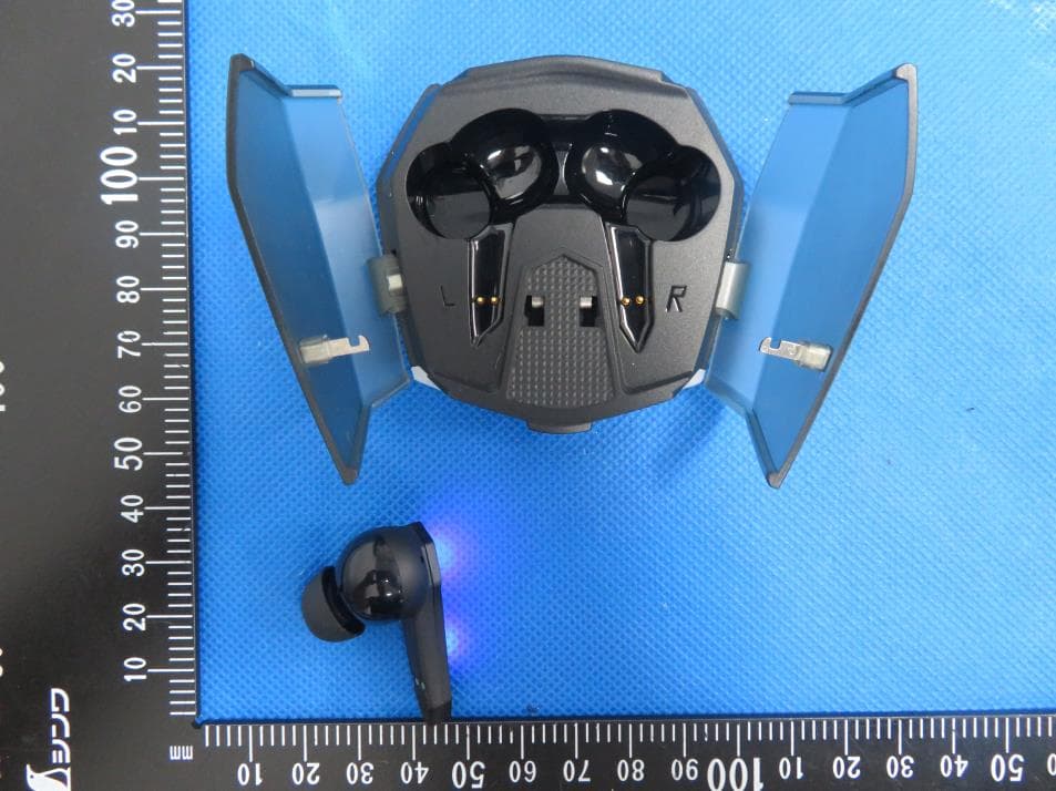
Click to zoom
Application Details
- Equipment Class
- DSS - Part 15 Spread Spectrum Transmitter
- Date of Grant
- Jul 17, 2024
- Application Purpose
- Original Equipment
- Date of Application
- Jul 16, 2024
- Equipment Note
- TW04G Wireless Earbuds
- Frequency Range
- 2402.00000000 - 2480.00000000
- Country
- China
Documents & Files
Document Text
Text extracted from the exhibit documents filed with the FCC. Open a document above to read the original.
Users Manual
开关 手动开机 长按左右耳机MFB键3秒 耳机开机并伴有提示音 打开充电盒耳机自动开机 自动开机 长按左右耳机MFB键5秒耳机关机 并伴有提示音.(左右耳机TWS组队状态, 长按任意一边仅单耳关机,另一边耳机仍正常工作) 放入充电盒中关闭充电盒上盖, 耳机自动关机并开始充电 手动关机 自动关机 按键区域 蓝牙连接 从充电盒中拿起两个耳机 TW04G 无线耳机说明书 Wir eless Earbuds Instructions Netac TW04G Netac TW04G 型号:TW04G 耳机电池:40mAh 充电仓电池:400mAh 播放时间:5.5H(耳机) +22H(充电仓) 充电时长:1.5H 产品重量:49±5g 扬声器单元:φ13mm 输入:DC5V 450mA 注意事项 请在常温环境中存放以及使用本产品; 请勿将本产品长期暴露在雨中或潮湿的环境中; 请勿丢掷,避免因跌落造成产品破坏; 请勿自行拆解、修理和改造本产品; 请使用额定电压的电源充电器充电; 擅自拆解将使保修失效。 充电盒及耳机内的电池为不可更换电池 不得暴露在诸如日照、火烤或类似过热的环境中 matt er s needing attention Please stor e and use this product in normal t emperature environment; Do not expose this product to rain or humid environment for a long time; Do not throw it to av oid product damage caused by falling; Do not disassemble, rep air or transform this product by your self ; Please use the power charger with rated v oltage to charge; Unauthorized disassembly will invalidate the warranty. The batt eries in the charging stand and earphone are non replaceable batt eries Do not expose to such conditions as sunlight, fire or similar overheating Model:TW04G Earbud Battery:40mAh Charging Case:400mAh Play Time:5.5H(Earbuds) +22H(Charging Case) Charging Time:1.5H Product Weight:49±5g Speaker Unit:φ13mm Input:DC5V 450mA 延期服务及更多礼遇 敬请关注朗科官方订阅号 北京朗科创新技术发展有限公司 地址:北京市门头沟区石龙经济开发区永安路20号3号楼一层138室 深圳市朗科科技股份有限公司 地址:深圳市南山区高新区南区高新南六道10号朗科大厦 服务电话:400-105-5505 官方网址:www.netac.com.cn Beijing Netac Innovation Technology Development Co.,Ltd. Location:138-1-3 No.20,Yongan Road,Mentougou District,Beijing,China Netac Technology Co.,Ltd. Location:Netac Building,Number 6 High-tech South St,Nanshan District, Shenzhen,P.R.China 518057 Web:www.netac.com FCC Compliance S tatement Thi s d evice c omplies with part 15 of the FCC Rul es. Oper ation is subject to the follo wing two c onditions: (1) This devic e may not c ause harmful interf er enc e. (2) Thi s device m ust acce pt any interf erenc e received, inclu ding int erf er enc e tha t may cause undesired operation. This equipment has been test ed and found to comply with the limits for a Class B digital de vice, pu rsua nt to part 15 o f the FCC Rules. These limit s ar e designed to pr ovide reasonable prot ection against harmful int erference in a residen tial i nstalla tion. Th is e quipment g ener ates uses and can radiate r adio frequency ene rgy and, if not inst alled and used in acco rdance w ith the instru ctions, may cause harmful interfer- ence to r adio communications. However, the re is no guarant ee tha t interf erenc e wi ll not oc cur i n a particular installa tion. If t his equ ipm ent does cause harmfu l int erf erenc e t o radi o or t ele vision reception, which can be determined b y turning the equipment off and on, the user is enc our aged to try to c orr ect the interf erenc e by one or more of the follo wing measur es: -R eorient or reloc ate the rec eiving antenna. -Incr ease the separ ation betw een the equipment and rec eiv er . -Connect the equi pment into an outlet on a cir cuit different from that to which the rec eiv er is connected. -Consult the dealer or an experienced r adio/TV technician for help. 保修卡 感谢您选择朗科产品。通过正规渠道购买的朗科产品依法享有国家规定的三 包服务。查询具体细则请登录朗科中文网站:http://www.netac.com.cn 自签收之日起,朗科无线蓝牙/有线耳机配件齐全且无人为损坏,享有七天无 理由退货,十五天换货,一年非人为有性能故障保修服务(有线耳机一年半)。 产品名称 产品SN码 顾客姓名 联系电话 联系地址 购买日期 保修日期故障及处理方法 用户资料 保修记录 完成日期顾客签名 128g铜版纸 正面第一页 背面第一页 TW04G尺寸77mm x 585mm EARBUDS earbuds earbuds earbuds Auto startup Auto shutdown Press and hold the MFB button on the left and right headphones for about 5 seconds to turn off the device, accompanied by a beep. (When Left and right earbuds are connect, Long press L/R earbud to turn off the related earbud, the another earbud still works normally) Manual shutdown Manual startup 耳机在未连接状态下,同时长按左右耳机5秒MFB键, 耳机清除TWS组队和设备配对记录成功。 耳机电量低时伴有提示音,请及时放入仓内充电。 When the earbud batter y is low with warning tone. Ple ase put it into the charge c ase t o charge it in time. When the earbuds are not connected, hold left and right earbuds MFB button 5 seconds to clear the TWS pairing and device pairing records. 同时长按左右耳5秒 Hold on left and right ear buds 5s FCC Caution: This device complies with part 15 of the FCC Rules. Operation is subject to the following two conditions: (1) This device may not cause harmful interference, and (2) this device must accept any interference received, including interference that may cause undesired operation. Any Changes or modifications not expressly approved by the party responsible for compliance could void the user's authority to operate the equipment. Note: This equipment has been tested and found to comply with the limits for a Class B digital device, pursuant to part 15 of the FCC Rules. These limits are designed to provide reasonable protection against harmful interference in a residential installation. This equipment generates uses and can radiate radio frequency energy and, if not installed and used in accordance with the instructions, may cause harmful interference to radio communications. However, there is no guarantee that interference will not occur in a particular installation. If this equipment does cause harmful interference to radio or television reception, which can be determined by turning the equipment off and on, the user is encouraged to try to correct the interference by one or more of the following measures: -Reorient or relocate the receiving antenna. -Increase the separation between the equipment and receiver. -Connect the equipment into an outlet on a circuit different from that to which the receiver is connected. -Consult the dealer or an experienced radio/TV technician for help. The device has been evaluated to meet general RF exposure requirement. The device can be used in portable exposure condition without restriction.
Attestation Statements
U.S.AgentDesignationforServiceofProcess (ApplicantandU.S.AgentareSeparateParties) TO:FederalCommunicationsCommission 7435OaklandMillsRoad Columbia,MD21046 ATTENTION:FCCCertification–Section2.911(d)(7)Information DesignatedU.S.Agent CompanyName:HOPEKCORPORATIONINC Address:4358SBANNOCKSTENGLEWOOD,CO80110UnitedStates FRN:0034562900 ContactName:PeterDavis Tel.:561-235-6113 Email:[email protected] Thisletteristoconfirmthatwe(“theDesignatedU.S.Agent)haveacceptedtheresponsibilitytoactasthe DesignatedU.S.AgentforServiceofProcessasrequiredbysection47CFR2.911(d)(7)onbehalfofthe Applicantnotedbelow. U.S.AgentSignature: Date: Signedby(PrintedName/Title): TheApplicantacknowledgesthattheymustmaintainanagentfornolessthanoneyearafterterminatingall marketingandimportationORtheconclusionofanyCommission-relatedproceedinginvolvingthe equipment.TheapplicantfurtheracknowledgestheirresponsibilitytoinformtheFCCwheneverthe DesignatedU.S.Agentinformationabovechanges. Applicant Companyname:BeijingNetacInnovationTechnologyDevelopmentCo.,Ltd. FRN:0034670349 GranteeCode:2BEBP FCCID:2BEBP-TW04G ContactName:dongdongxie StreetAddress:138-1-3NO.20YONGANROADMENTOUGOUDISTRICTBEIJINGCHINA TelephoneNo:13612842510 Email:[email protected] ApplicantSignature: Date:July11,2024 Signedby(PrintedName/Title):dongdongxie/Manager
Attestation Statements
Beijing Netac Innovation Technology Development Co.,Ltd. 2024.06.11 Eurofins Electrical and Electronic Testing NA, Inc. 914 West Patapsco Avenue Baltimore, MD 21230 RE: Attestation Statements Part 2.911(d)(5)(i) request for FCC ID: 2BEBP-TW04G [Beijing Netac Innovation Technology Development Co.,Ltd.] (“the applicant”) certifies that the equipment for which authorization is sought is not “covered” equipment prohibited from receiving an equipment authorization pursuant to section 2.903 of the FCC rules. Sincerely, (Applicant signature) (Applicant printed name) Dongdong xie Beijing Netac Innovation Technology Development Co.,Ltd. 2024.06.11 Eurofins Electrical and Electronic Testing NA, Inc. 914 West Patapsco Avenue Baltimore, MD 21230 RE: Attestation Statements Part 2.911(d)(5)(ii) request for FCC ID: 2BEBP-TW04G [Beijing Netac Innovation Technology Development Co.,Ltd.] (“the applicant”) certifies that, as of the date of the filing of the application, the applicant is not identified on the Covered List as an entity producing “covered” equipment. Sincerely, (Applicant signature) (Applicant printed name) Dongdong xie
Cover Letter(s)
Beijing Netac Innovation Technology Development Co.,Ltd. 2024.06.11 Eurofins Electrical and Electronic Testing NA, Inc. 914 W. Patapsco Avenue Baltimore, MD 21230 USA RE: CONFIDENTIALITY REQUEST FOR EUT NAME: TW04G Wireless Earbuds Trademark: Netac MODEL : TW04G FCC ID : 2BEBP-TW04G To Whom It May Concern: This letter serves as an official request for confidentiality under sections 0.457 and 0.459 of CFR 47. We have requested that the - Block Diagram - Schematics - Operational Description required to be submitted with this application be permanently withheld from public review. The above materials contain trade secrets and proprietary information not customarily released to the public. The public disclosure of these materials may be harmful to the applicant and provide unjustified benefits to its competitors. Please contact me if there is any information you may need. Sincerely, Client’s signature: Client’s name / title : Dongdong xie /Manager Contact information / address: 138-1-3 NO.20 YONG AN ROAD MEN TOU GOU DISTRICT BEIJING CHINA
Cover Letter(s)
Beijing Netac Innovation Technology Development Co.,Ltd. 2024.06.11 Eurofins Electrical and Electronic Testing NA, Inc. 914 W. Patapsco Avenue Baltimore, MD 21230 USA RE: LETTER OF AGENT AUTHORIZATION To Whom It May Concern: We, the undersigned, hereby authorize Shenzhen BCTC Testing Co., Ltd to act on our behalf in all matters relating to application for equipment authorization, including the signing of all documents relating to these matters. We also hereby certify that no party to the application authorized hereunder is subject to the denial of benefits, including FCC benefits, pursuant to Section 5301 of the Anti-Drug Abuse Act of 1988, 21 U.S.C.853(a). This agreement expires one year from the current date. Sincerely, Client’s signature: Client’s name / title : dongdong xie /Manager Contact information / address: 138-1-3 NO.20 YONG AN ROAD MEN TOU GOU DISTRICT BEIJING CHINA
External Photos
External Photos
ID Label/Location Info
Size:10*5mm FCC ID: 2BEBP-TW04G Label location
Internal Photos
Internal Photos Antenna
RF Exposure Info
RF EXPOSURE EVALUATION METHOD FCC ID:2BEBP-TW04G Applicable standard: In accordance with FCC 47 CFR part 2 (2.1093) this device has been defined as a portable device which is defined as a transmitting device designed to be used so that the radiating structure(s) of the device is/are within 20 centimeters of the body of the user. Portable devices must be evaluated using the specified in FCC 47 CFR part 2 (2.1093) and ANSI/IEEEC95.1-1992. and had been tested in accordance with the measurement methods and procedures specified in IEEE 1528-2003. Per FCC KDB 447498 D01 v06, the 1-g and 10-g SAR test exclusion thresholds for 100 MHz to 6 GHz at test separation distances s 50 mm are determined by: SAR Test Exclusion Thresholds for 100 MHz – 6 GHz and ≤ 50 mm Approximate SAR Test Exclusion Power Thresholds at Selected Frequencies and Test Separation Distances are illustrated in the following Table. The 1-g and 10-g SAR test exclusion thresholds for 100 MHz to 6 GHz at test separation distances ≤ 50 mm are determined by: [(max. power of channel, including tune-up tolerance, mW)/(min. test separation distance, mm)] · [√f(GHz)] ≤ 3.0 for 1-g SAR and ≤ 7.5 for 10-g extremity SAR,where f(GHz) is the RF channel transmit frequency in GHz Power and distance are rounded to the nearest mW and mm before calculation The result is rounded to one decimal place for comparison The test exclusions are applicable only when the minimum test separation distance is ≤ 50 mm and for transmission frequencies between 100 MHz and 6 GHz. When the minimum test separation distance is < 5 mm, a distance of 5 mm is applied to determine SAR test exclusion. BT GFSK 2402 3.55 21 GFSK 2441 2.63 21 GFSK 2480 1.3 21 π/ 4 DQPSK 2402 4.05 21 π/ 4 DQPSK 2441 3.18 21 π/ 4 DQPSK 2480 1.89 21 8DPSK 2402 4.28 21 8DPSK 2441 3.41 21 8DPSK 2480 2.16 21 max possible output power (PK,conducted):5±1dBm 2.11dBi logarithmic terms convert to numeric result is nearly 1.63 6dBm=3.98mW 2402MHz [(max. power of channel, including tune-up tolerance, mW)/(min. test separation distance,mm)] · [√f(GHz)]= 3.98/5*√2.402=1.23≤3.0 2441MHz [(max. power of channel, including tune-up tolerance, mW)/(min. test separation distance,mm)] · [√f(GHz)]= 3.98/5*√2.441=1.24≤3.0 2480MHz [(max. power of channel, including tune-up tolerance, mW)/(min. test separation distance,mm)] · [√f(GHz)]= 3.98/5*√2.48=1.25≤3.0 Conclusion: 1. [(max. power of channel, including tune-up tolerance, mW)/(min. test separation distance, mm)] * [√f(GHz)] < 3.0. 2. SAR Test Exclusion Thresholds is 3.0 for separation distance 5mm. Therefore, SAR test is not required.
Test Report
Features 1.Surface Mounted Devices with a small dimension of 2.0 x 1.25 x 0.25 mm 3 meet future miniaturization trend. 2.Embedded and (Low Temperature Co-fired Ceramic) technology is able to future integrate with system design as well as beautifying the housing of final product. 3.High Stability in Temperature / Humidity Change Applications 1. Bluetooth 2. Wireless LAN 3. HormRF 4. ISM band 2.4GHz wireless applications Dimensions(Unit:mm) H L X 20125025 A03 Dimension (mm) L 2.0 ± 0.20 W 1.2 ± 0.20 T 0.25 ± 0.05 Manufacturer:Beijing Netac Innovation Tec hnology Development Co.,Ltd. Type2 : Type3 : PCB Bottom View : H L X 20125025 A03 Evaluation Board and Matching Circuits Electrical Characteristics H L X 20125025 A03 Specification Part NumberANTD21W02-X1 Central Frequency2450MHz Bandwidth90 (Min.)MHz Return Loss-10 (Max)dB Peak Gain2.11dBi Impedance50 Ω Operating Temperature -40~+85 °C Maximum Power1W Resistance to Soldering Heats 10 ( @ 260°C) sec. PolarizationLinear Azimuth BeamwidthOmni-directional TerminationCu / Sn (Leadless) Characteristic curve Radiation Pattern H L X 20125025 A03 Frequency (MHz)240024502500 Efficiency (dB)-1.42-1.24-1.47 Efficiency (%)717571 Peak Gain (dBi)2.112.061.94 Reliability and Test Condictions Phase Temperature(°C) Time(min) 1 +85±5°C 30±3 2 Room Temperature Within 3sec 3 -40±2°C 30±3 4 Room Temperature Within 3sec ITEMREQUIREMENTSTEST CONDITION Solderability 1.Wetting shall exceed 90% coverage 2.No visible mechanical damage TEMP (°C) 230°C 4±1 sec. 150°C 60sec Pre-heating temperature:150°C/60sec. Solder temperature:230±5°C Duration:4±1sec. Solder:Sn-Ag3.0-Cu0.5 Flux for lead free: rosin Solder heat Resistance 1.No visible mechanical damage 2.Central Freq. change :within ± 6% TEMP (°C) 260°C 10±0.5 sec. 150°C 60sec Pre-heating temperature:150°C/60sec. Solder temperature:260±5°C Duration:10±0.5sec. Solder:Sn-Ag3.0-Cu0.5 Flux for lead free: rosin Component Adhesion (Push test) 1. No visible mechanical damageThe device should be reflow soldered(230±5°C for 10sec.) to a tinned copper substrate A dynometer force gauge should be applied the side of the component. The device must with-ST-F 0.5 Kg without failure of the termination attached to component. Component Adhesion (Pull test) 1. No visible mechanical damage Insert 10cm wire into the remaining open eye bend ,the ends of even wire lengths upward and wind together. Terminal shall not be remarkably damaged. Thermal shock 1.No visible mechanical damage 2.Central Freq. change :within ±6% +85°C=>30±3min -40°C=>30±3min Test cycle:10 cycles The chip shall be stabilized at normal condition for 2~3 hours before measuring. Resistance to High Temperature 1.No visible mechanical damage 2.Central Freq. change :within ±6% 3.No disconnection or short circuit. Temperature: 85±5°C Duration: 1000±12hrs The chip shall be stabilized at normal condition for 2~3 hours before measuring. Resistance to Low Temperature 1.No visible mechanical damage 2.Central Freq. change :within ±6% 3.No disconnection or short circuit. Temperature:-40±5°C Duration: 1000±12hrs The chip shall be stabilized at normal condition for 2~3 hours before measuring. Humidity 1.No visible mechanical damage 2.Central Freq. change :within ±6% 3.No disconnection or short circuit. Temperature: 40±2°C Humidity: 90% to 95% RH Duration: 1000±12hrs The chip shall be stabilized at normal condition for 2~3 hours before measuring. H L X 20125025 A03 Soldering and Mounting Mildly activated rosin fluxes are preferred. The minimum amount of solder can lead to damage from the stresses caused by the difference in coefficients of expansion between solder, chip and substrate. The terminations are suitable for all wave and re-flow soldering systems. If hand soldering cannot be avoided, the preferred technique is the utilization of hot air soldering tools. Recommended temperature profiles for re-flow soldering in Figure 1. Products attachment with a soldering iron is discouraged due to the inherent process control limitations. In the event that a soldering iron must be employed the following precautions are recommended. ‧Preheat circuit and products to 150°C ‧Never contact the ceramic with the iron tip ‧Use a 20 watt soldering iron with tip diameter of 1.0mm ‧280°C tip temperature (max) ‧1.0mm tip diameter (max) ‧Limit soldering time to 3 sec. NATURAL COOLING PRE-HEATING 60~120 s SOLDERING 10s max. 30~60s 250~260 230 180 150 TIME(sec.) Reflow Soldering NATURAL COOLING PRE-HEATINGSOLDERING within 3s Gradual cooling 150 TIME(sec.) Iron Soldering Over 60s 350 300 H L X 20125025 A03 Packaging Information ◆Tape Specification: ◆Reel Specification: (7’’, Φ180 mm) Tape Width(mm)A(mm)B(mm)C(mm)D(mm)Chip/Reel(pcs) 8 9.0±0.560±213.5±0.5178±2 6000 H L X 20125025 A03 Storage and Transportation Information Storage Conditions To maintain the solderability of terminal electrodes: 1.Temperature and humidity conditions: -10~ 40°C and 30~70% RH. 2.Recommended products should be used within 6 months from the time of delivery. 3.The packaging material should be kept where no chlorine or sulfur exists in the air. Transportation Conditions 1.Products should be handled with care to avoid damage or contamination from perspiration and skin oils. 2.The use of tweezers or vacuum pick up is strongly recommended for individual components. 3.Bulk handling should ensure that abrasion and mechanical shock are minimized. H L X 20125025 A03
Test Report
No.:BCTC/RF-EMC-005 Page: 1 of 79 Edition:B.2 TEST REPORT Shenzhen BCTC Testing Co., Ltd. Report No.: BCTC2405862595E Applicant: Beijing Netac Innovation Technology Development Co.,Ltd. Product Name: TW04G Wireless Earbuds Test Model: TW04G Tested Date: 2024-05-22 to 2024-05-28 Issued Date: 2024-05-29 Report No.:BCTC2405862595E No.:BCTC/RF-EMC-005 Page: 2 of 79 Edition:B.2 FCC ID:2BEBP-TW04G The test report is effective only with both signature and specialized stamp. This result(s) shown in this report refer only to the sample(s) tested. Without written approval of Shenzhen BCTC Testing Co., Ltd, this report can’t be reproduced except in full. The tested sample(s) and the sample information are provided by the client. Product Name: TW04G Wireless Earbuds Trademark: Netac Model/Type Reference: TW04G Prepared For: Beijing Netac Innovation Technology Development Co.,Ltd. Address: 138-1-3 NO.20 YONG AN ROAD MEN TOU GOU DISTRICT BEIJING CHINA Manufacturer: Beijing Netac Innovation Technology Development Co.,Ltd. Address: 138-1-3 NO.20 YONG AN ROAD MEN TOU GOU DISTRICT BEIJING CHINA Prepared By: Shenzhen BCTC Testing Co., Ltd. Address: 1-2/F., Building B, Pengzhou Industrial Park, No.158, Fuyuan 1st Road, Zhancheng, Fuhai Subdistrict, Bao'an District, Shenzhen, Guangdong, China Sample Received Date: 2024-05-22 Sample tested Date: 2024-05-22 to 2024-05-28 Issue Date: 2024-05-29 Report No.: BCTC2405862595E Test Standards FCC Part15.247 ANSI C63.10-2013 Test Results PASS Remark: This is Bluetooth Classic radio test report. Tested by: Approved by: Tang Changyu/ Project Handler Zero Zhou/Reviewer Report No.:BCTC2405862595E No.:BCTC/RF-EMC-005 Page: 3 of 79 Edition:B.2 Table Of Content Test Report Declaration Page 1. Version .................................................................................................................. 5 2. Test Summary ....................................................................................................... 6 3. Measurement Uncertainty ..................................................................................... 7 4. Product Information And Test Setup ..................................................................... 8 4.1 Product Information ............................................................................................... 8 4.2 Test Setup Configuration ...................................................................................... 8 4.3 Support Equipment ............................................................................................... 9 4.4 Channel List .......................................................................................................... 9 4.5 Test Mode ........................................................................................................... 10 4.6 Table Of Parameters Of Text Software Setting ................................................... 10 5. Test Facility And Test Instrument Used ............................................................... 11 5.1 Test Facility ......................................................................................................... 11 5.2 Test Instrument Used .......................................................................................... 11 6. Conducted Emissions .......................................................................................... 13 6.1 Block Diagram Of Test Setup .............................................................................. 13 6.2 Limit .................................................................................................................... 13 6.3 Test procedure .................................................................................................... 13 6.4 EUT operating Conditions ................................................................................... 13 6.5 Test Result .......................................................................................................... 14 7. Radiated emissions ............................................................................................. 16 7.1 Block Diagram Of Test Setup .............................................................................. 16 7.2 Limit .................................................................................................................... 17 7.3 Test procedure .................................................................................................... 18 7.4 EUT operating Conditions ................................................................................... 19 7.5 Test Result .......................................................................................................... 19 8. Radiated Band Emission Measurement And Restricted Bands Of Operation ..... 23 8.1 Block Diagram Of Test Setup .............................................................................. 23 8.2 Limit .................................................................................................................... 23 8.3 Test procedure .................................................................................................... 24 8.4 EUT operating Conditions ................................................................................... 24 8.5 Test Result .......................................................................................................... 25 9. Spurious RF Conducted Emissions ..................................................................... 26 9.1 Block Diagram Of Test Setup .............................................................................. 26 9.2 Limit .................................................................................................................... 26 9.3 Test procedure .................................................................................................... 26 9.4 Test Result ........................................................................................…
Text truncated - open the document above for the full version.
Test Report
Report No.:BCTC2405862595E No.:BCTC/RF-EMC-005 Page: 56 of 79 Edition:B.2 Power NVNT 1-DH1 2480MHz Power NVNT 2-DH1 2402MHz Report No.:BCTC2405862595E No.:BCTC/RF-EMC-005 Page: 57 of 79 Edition:B.2 Power NVNT 2-DH1 2441MHz Power NVNT 2-DH1 2480MHz Report No.:BCTC2405862595E No.:BCTC/RF-EMC-005 Page: 58 of 79 Edition:B.2 Power NVNT 3-DH1 2402MHz Power NVNT 3-DH1 2441MHz Report No.:BCTC2405862595E No.:BCTC/RF-EMC-005 Page: 59 of 79 Edition:B.2 Power NVNT 3-DH1 2480MHz Report No.:BCTC2405862595E No.:BCTC/RF-EMC-005 Page: 60 of 79 Edition:B.2 12. Hopping Channel Separation 12.1 Block Diagram Of Test Setup 12.2 Limit Frequency hopping systems shall have hopping channel carrier frequencies separated by a minimum of 25 kHz or the 20 dB bandwidth of the hopping channel, whichever is greater. Alternatively, frequency hopping systems operating in the 2400-2483.5 MHz band may have hopping channel carrier frequencies that are separated by 25 kHz or two-thirds of the 20 dB bandwidth of the hopping channel, whichever is greater, provided the systems operate with an output power no greater than 0.125W. 12.3 Test procedure 1. Remove the antenna from the EUT and then connect a low RF cable from the antenna port to the spectrum. 2. Set the spectrum analyzer: RBW = 30kHz. VBW = 100kHz , Span = 2.0MHz. Sweep = auto; Detector Function = Peak. Trace = Max hold. 3. Allow the trace to stabilize. Use the marker-delta function to determine the separation between the peaks of the adjacent channels. The limit is specified in one of the subparagraphs of this Section Submit this plot. 12.4 Test Result Temperature: 26°C Relative Humidity: 54% Test Voltage: DC 3.7V Remark: N/A Condition Mode Hopping Freq1 (MHz) Hopping Freq2 (MHz) HFS (MHz) Limit (MHz) Verdict NVNT 1-DH1 2401.872 2402.872 1 0.607 Pass NVNT 1-DH1 2440.872 2441.872 1 0.606 Pass NVNT 1-DH1 2478.868 2479.872 1.004 0.571 Pass NVNT 2-DH1 2401.87 2402.87 1 0.841 Pass NVNT 2-DH1 2440.87 2441.87 1 0.833 Pass NVNT 2-DH1 2478.872 2479.87 0.998 0.839 Pass NVNT 3-DH1 2402.018 2403.02 1.002 0.812 Pass NVNT 3-DH1 2441.022 2442.026 1.004 0.812 Pass NVNT 3-DH1 2479.028 2480.026 0.998 0.806 Pass Report No.:BCTC2405862595E No.:BCTC/RF-EMC-005 Page: 61 of 79 Edition:B.2 Test Graphs CFS NVNT 1-DH1 2402MHz CFS NVNT 1-DH1 2441MHz Report No.:BCTC2405862595E No.:BCTC/RF-EMC-005 Page: 62 of 79 Edition:B.2 CFS NVNT 1-DH1 2480MHz CFS NVNT 2-DH1 2402MHz Report No.:BCTC2405862595E No.:BCTC/RF-EMC-005 Page: 63 of 79 Edition:B.2 CFS NVNT 2-DH1 2441MHz CFS NVNT 2-DH1 2480MHz Report No.:BCTC2405862595E No.:BCTC/RF-EMC-005 Page: 64 of 79 Edition:B.2 CFS NVNT 3-DH1 2402MHz CFS NVNT 3-DH1 2441MHz Report No.:BCTC2405862595E No.:BCTC/RF-EMC-005 Page: 65 of 79 Edition:B.2 CFS NVNT 3-DH1 2480MHz Report No.:BCTC2405862595E No.:BCTC/RF-EMC-005 Page: 66 of 79 Edition:B.2 13. Number Of Hopping Frequency 13.1 Block Diagram Of Test Setup 13.2 Limit Frequency hopping systems in the 2400-2483.5 MHz band shall use at least 15 channels. 13.3 Test procedure 1. Remove the antenna from the EUT and then connect a low RF cable from the antenna port to the spectrum. 2. Set the spectrum analyzer: RBW = 100kHz. VBW = 300kHz. Sweep = auto; Detector Function = Peak. Trace = Max hold. 3. Allow the trace to stabilize. It may prove necessary to break the span up to sections. in order to clearly show all of the hopping frequencies. The limit is specified in one of the subparagraphs of this Section. 4. Set the spectrum analyzer: Start Frequency = 2.4GHz, Stop Frequency = 2.4835GHz. Sweep=auto; 13.4 Test Result Temperature: 26°C Relative Humidity: 54% Test Voltage: DC 3.7V Remark: N/A Condition Mode Hopping Number Limit Verdict NVNT 1-DH1 79 15 Pass NVNT 2-DH1 79 15 Pass NVNT 3-DH1 79 15 Pass Report No.:BCTC2405862595E No.:BCTC/RF-EMC-005 Page: 67 of 79 Edition:B.2 Test Graphs Hopping No. NVNT 1-DH1 2441MHz Hopping No. NVNT 2-DH1 2441MHz Report No.:BCTC2405862595E No.:BCTC/RF-EMC-005 Page: 68 of 79 Edition:B.2 Hopping No. NVNT 3-DH1 2441MHz Report No.:BCTC2405862595E No.:BCTC/RF-EMC-005 Page: 69 of 79 Edition:B.2 14. Dwell Time 14.1 Block Diagram Of Test Setup 14.2 Limit Frequency hopping systems in the 2400-2483.5 MHz band shall use at least 15 channels. The average time of occupancy on any channel shall not be greater than 0.4 seconds within a period of 0.4 seconds multiplied by the number of hopping channels employed. Frequency hopping systems may avoid or suppress transmissions on a particular hopping frequency provided that a minimum of 15 channels are used. 14.3 Test procedure 1. Remove the antenna from the EUT and then connect a low RF cable from the antenna port to the spectrum. 2. Set spectrum analyzer span = 0. Centred on a hopping channel; 3. Set RBW = 1MHz and VBW = 3MHz.Sweep = as necessary to capture the entire dwell time per hopping channel. Set the EUT for DH5, DH3 and DH1 packet transmitting. 4. Use the marker-delta function to determine the dwell time. If this value varies with different modes of operation (e.g.. data rate. modulation format. etc.). repeat this test for each variation. The limit is specified in one of the subparagraphs of this Section. Submit this plot(s). 14.4 Test Result DH5 Packet permit maximum 1600 / 79 / 6 hops per second in each channel (5 time slots RX, 1 time slot TX). DH3 Packet permit maximum 1600 / 79 / 4 hops per second in each channel (3 time slots RX, 1 time slot TX). DH1 Packet permit maximum 1600 / 79 /2 hops per second in each channel (1 time slot RX, 1 time slot TX). So, the Dwell Time can be calculated as follows: DH5:1600/79/6*0.4*79*(MkrDelta)/1000 DH3:1600/79/4*0.4*79*(MkrDelta)/1000 DH1:1600/79/2*0.4*79*(MkrDelta)/1000 Remark: Mkr Delta is once pulse time. Report No.:BCTC2405862595E No.:BCTC/RF-EMC-005 Page: 70 of 79 Edition:B.2 Tempera…
Text truncated - open the document above for the full version.
Contact Information
Applicant
dongdong xie
Test Firm
Shenzhen BCTC Testing Co., Ltd.Sally He
[email protected]15999690624
Technical Specifications
| # | Rule Parts | Frequency Range | Power Output |
|---|---|---|---|
| 1 | 15C | 2.40 GHz - 2.48 GHz | 2.68 mW |
Other Applications from Beijing Netac Innovation Technology Development Co.Ltd
2BEBP-TW06
Jul 15, 2024True wireless earbuds
Equipment Class
DSS - Part 15 Spread Spectrum Transmitter2BEBP-LK56
Jul 11, 2024Wireless Earbuds
Equipment Class
DTS - Digital Transmission System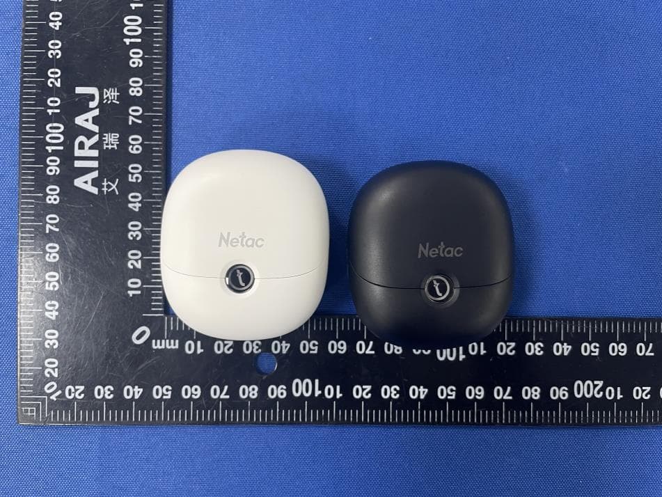
2BEBP-ACE01
Jul 01, 2024Wireless Earbuds
Equipment Class
DSS - Part 15 Spread Spectrum Transmitter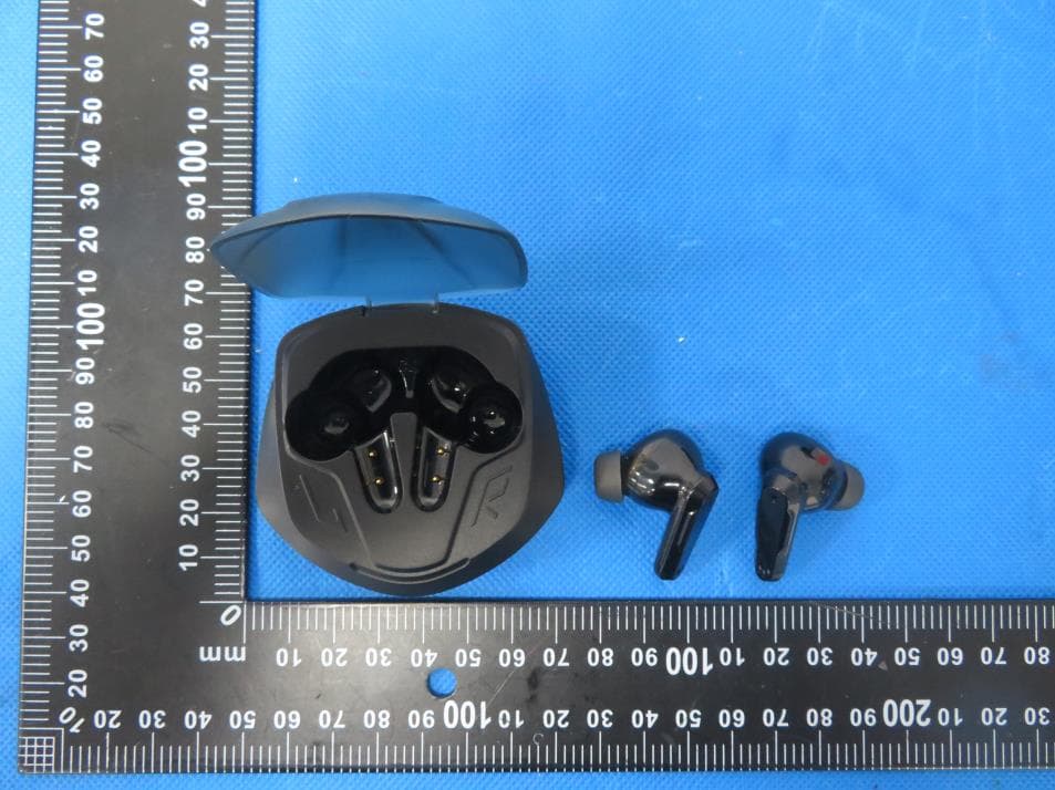
2BEBP-TW03G
Jun 29, 2024TW03G Wireless Earbuds
Equipment Class
DSS - Part 15 Spread Spectrum Transmitter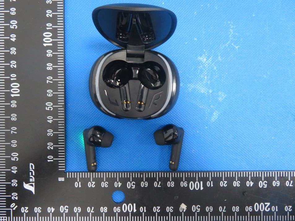
2BEBP-TW02G
Jun 27, 2024Wireless Earbuds
Equipment Class
DSS - Part 15 Spread Spectrum Transmitter