A2HWL0217WiFi Module
Alco Electronics Ltd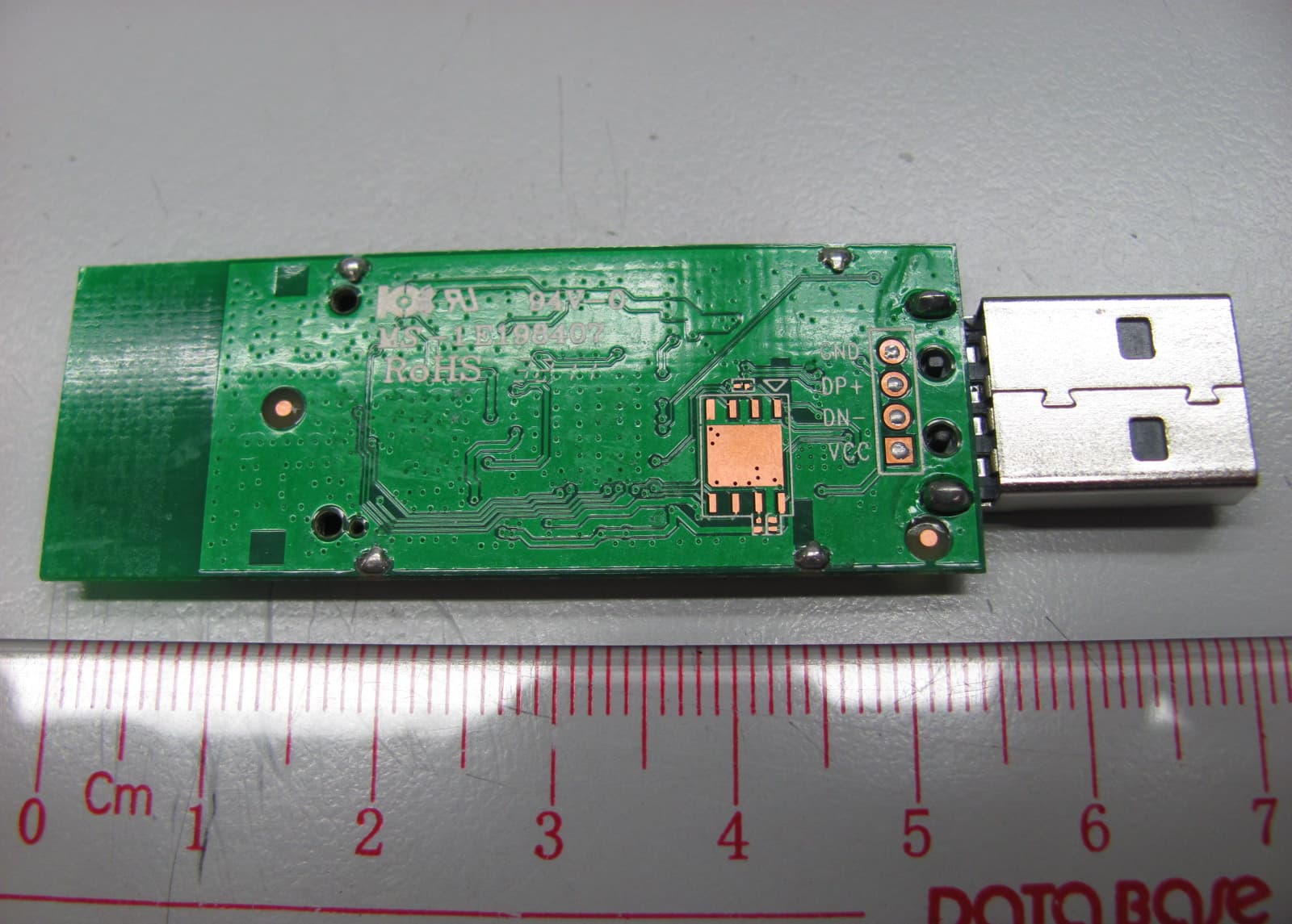
Click to zoom
Application Details
- Equipment Class
- DXX - Part 15 Low Power Communication Device Transmitter
- Date of Grant
- Nov 02, 2011
- Application Purpose
- Original Equipment
- Date of Application
- Nov 02, 2011
- Equipment Note
- WiFi Module
- Frequency Range
- 2412.00000000 - 2462.00000000
- Company
- Alco Electronics Ltd
- Country
- Hong Kong
Documents & Files
Document Text
Text extracted from the exhibit documents filed with the FCC. Open a document above to read the original.
Users Manual
WiFi MODULE WL0217 (IEEE 802.11b/g/n), WL0217 user’s manual 1. Install the driver a. Insert the installation CD into your CD-ROM driver,Double click the icon to start setup. b. c. Choose Broadcom configuration Tool and click next to go on d. Choose optimize for wifi mode and click next to go on e. Choose Click Install to begin the installation and click Install to go on f. Click Finish to end the setup 2. Plug in your usb wireless LAN adapter,it will be recognized and auto installed..Just confirmed it like below: 3. Make infrastructure connection Double click the icon in red circle You will see: You can click the button Rescan to find which AP is in range,the will show on the window,choice one you want to connect,and click the button connect. An infrastructure connection is accomplished. Note,please choose correct channel setting up to your law,for example,ch13 is permitted in your country,and you set your router at ch13,while you choose ch1-ch11(default setting),you will never find the AP,and you will have to choose ch1-ch13 seting in Advanced page as below. 4. Some help information in Broacom Wireless utility ● How to find out your ip address: 5.Mske Ad-hoc mode connection ●Mske an Ad-hoc SSID ● A ● B ● C 5.2 Setup static IP address for the AD-Hoc link ●A At its property page,double click item Internet Protocol(TCP/IP) ● B You will get ● C Fill the IP address blank,example as below: ● D Click ok to finish the setup 5.3 Ad-Hoc setup for one point accomplished 5.4 Setup another Ad-hoc point as step A、B、 C、D. 5.5 Ad-hoc mode link accomplished.And you can visit each other. Note:To make an Ad-Hoc mode link.Do remember to choice the same channel.Its static IP address should be in the same netsub,and the SSID should be the same too. Installation Guide: 1. This RF Module can be mounted to the end product by USB port. 2. Please follow the USB pin assignment and dimension of RF module for the end product design. 3. Thick and short PCB trace for VDD and GND should be made. 4. Decoupling capacitor is recommended to place next to the VDD pin. 5. Make sure there are no metallic objects placed on to or below the RF module after it is installed. 6. Only trace antennas are allowed to be used when the RF module installed. 7. Make sure that the specified supply voltage is not exceeded. 8. Make sure that the power supply is clean (low noise and ripple). 9. Unused connection and test point on the transceiver module should be disconnected. 10. The RF module is self-sufficient to function without the need of external components. Important notes: Please note that the module is only approved for use when installed in devices produced by a specific manufacturer for professional installation. Important notes to third party user for transceiver module: The transceiver Module complies with Part15 of the FCC rules and regulations. Compliance with the labeling requirements, FCC notices and antenna usage guidelines is required. To fulfill FCC Certification, the third party user must comply with the following regulations: 1. The third party user must ensure that the text on the external label provided with this device is placed on the outside of the final product. Contains FCC ID: A2HWL0217. The enclosed device complies with Part 15 of the FCC Rules. Operation is subject to the following two conditions: (1) this device may not cause harmful interference, and (2) this device must accept any interference received, including interference that may cause undesired operation. 2. The transceiver Module may only be used with the onboard PCB trace antenna that have been tested and approved for use with this module. 3. The transceiver Module have been certified by the FCC for use with other products without any further certification. Modifications not approved by ALCO Electronics Ltd. could void the user’s authority to operate the equipment. 4. Third party users must test final product to comply with unintentional radiators before declaring compliance of their final product to Part 15 of the FCC Rules. FCC Statement: This device complies with Part 15 of the FCC Rules. Operation is subject to the following two conditions: (1) this device may not cause harmful interference, and (2) this device must accept any interference received, including interference that may cause undesired operation. Warning: Changes or modifications to this unit not expressly approved by the party responsible for compliance (MLB International Inc., P.O. Box 1535, Buffalo, NY 14226, Tel: 516-236-4556) could void the user's authority to operate the equipment. NOTE: This equipment has been tested and found to comply with the limits for a Class B digital device, pursuant to Part 15 of the FCC Rules. These limits are designed to provide reasonable protection against harmful interference in a residential installation. This equipment generates, uses and can radiate radio frequency energy and, if not installed and used in accordance with the instructions, may cause harmful interference to radio communications. However, there is no guarantee that interference will not occur in a particular installation. If this equipment does cause harmful interference to radio or television reception, which can be determined by turning the equipment off and on, the user is encouraged to try to correct the interference by one or more of the following measures: 1. Reorient or relocate the receiving antenna. 2. Increase the separation between the equipment and receiver. 3. Connect the equipment into an outlet on a circuit different from that to which the receiver is needed. 4. Consult the dealer or an experienced radio/TV technician for help.
Cover Letter(s)
Contains FCC ID: A2HWL0217
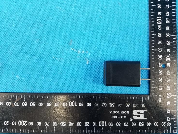
External Photos
INTERTEK TESTING SERVICE Report No.: HK11081162-1 FCC ID: A2HWL0217 Equipment Photographs Model : WL0217 (External)
Internal Photos
INTERTEK TESTING SERVICE Report No.: HK11081162-1 FCC ID: A2HWL0217 Equipment Photographs Model: WL0217 (Internal) INTERTEK TESTING SERVICE Report No.: HK11081162-1 FCC ID: A2HWL0217 Equipment Photographs Model: WL0217 (Internal)
Operational Description
Technical Description of Transceiver Module WL0217 The Equipment Under Test (EUT) is a WiFi transceiver module operating within the frequency band between 2412MHz and 2462MHz. It is intended to be used as short range radio communication for embedded application. The EUT is powered by USB port. The EUT has two identical trace antennas. (Antenna 0 and 1: Trace antenna, Internal, Integral) In 802.11b mode, the EUT employs Direct-Sequence Spread Spectrum (DSSS) modulation with maximum bit rate 11Mbps. Either one antenna is used (antenna 0 by default). In 802.11g mode, the EUT employs Orthogonal Frequency Division Multiplexing (OFDM) modulation with maximum bit rate 54Mbps. Either one antenna is used (antenna 0 by default). In 802.11n mode with 20MHz bandwidth, the EUT employs modulation type according to MCSn (Modulation and Coding Scheme) setting where n is 0 to 15, with maximum bit rate 65Mbps at n=7 and 130Mbps at n=15. Either one antenna is used (antenna 0 by default) when n=0 to 7. Both antennas are used simultaneously when n=8 to15 In 802.11n mode with 40MHz bandwidth, the EUT employs modulation type according to MCSn (Modulation and Coding Scheme) setting where n is 0 to 15, with maximum bit rate 150Mbps at n=7 and 300Mbps at n=15. Either one antenna is used (antenna 0 by default) when n=0 to 7. Both antennas are used simultaneously when n=8 to15 During 802.11b, 802.11g and 802.11n (20MHz bandwidth) mode, the EUT occupies 11 channels (2412MHz to 2462MHz). During 802.11n (40MHz bandwidth) mode, the EUT occupies 7 channels (2422MHz to 2452MHz). The modulation mode (802.11b/g/n20/n40), bit rate, channel selection, antenna selection and transmit power can be controlled by its control software. This module is only approved for use when installed in devices produced by a specific manufacturer for professional installation and within the specified bandwith and transmit power. 1. U1 (BCM43235KMLG) and its associated network acts as the transceiver module and USB host. U2 (MX25L3206EZNI-12G) is 4Mbyte flash memory incorporating with U1. 2. U3, U4, FL1, FL2 and associated network act as the RF front-end. U3, U4 are RF switches (SKY 13343-92LF) for switching between transmit and receive mode of RF front-end. FL1, FL2 are Low-Pass-Filter (DEA162500LT-1217A1) for 2.4GHz band. 3. U5 (PAM2306AYPAA) and its associated network act as the 3.3V DC regulator for the module. 8/23/2010 6LJAD Preliminary Data Sheet BCM43235 43235-DS02-R 5300 California Avenue • Irvine, CA 92617 • Phone: 949-926-5000 • Fax: 949-926-5203August 13, 2010 2.4 GHz 802.11n MAC/PHY/Radio Chip Figure 1: BCM43235 Block Diagram GENERAL DESCRIPTIONFEATURES The BCM43235 is a single-band (2.4 GHz) IEEE 802.11n-compliant MAC/PHY/Radio complete system-on-a-chip with a 2.4 GHz internal PA. The device enables the development of USB 2.0- or HSIC-based 802.11n WLAN client and router subsystem solutions. The BCM43235 is targeted for all WLAN markets that can take advantage of the high throughput and extended range of Broadcom’s second generation MIMO solution. With MIMO, information is sent and received over two or more antennas simultaneously using the same frequency band thus providing greater range and increasing throughput, while maintaining compatibility with legacy IEEE 802.11b/g devices. This is accomplished through a combination of enhanced MAC and PHY implementations including spatial multiplexing modes in the transmitter and receiver and advanced digital signal processing techniques to improve receive sensitivity. The BCM43235 architecture with its fully integrated single-band radio transceiver supports 2 × 2 antennas for Layer 2 throughput of over 200 Mbps. State-of-the-art security is provided by industry standardized system support for WPA™, WPA2™ (802.11i), and hardware accelerated AES encryption/decryption, coupled with TKIP and IEEE 802.1X support. Embedded hardware acceleration enables increased system performance and significant reduction in host-CPU utilization in both client and access point configurations. The BCM43235 also supports Broadcom’s widely accepted and deployed WPS for ease-of-use wireless secured networks. • IEEE 802.11n-compliant • 2.4 GHz internal PA • Two-stream spatial multiplexing up to 300 Mbps • Uses on-chip OTP (One-Time Programmable) memory instead of SROM for substantial RBOM savings. • Supports MCS 0–15 and MCS 32 modulation and coding rates. • Supports 20 MHz and 40 MHz channels with optional SGI. • Support for STBC in both TX and RX • Greenfield, mixed mode, and legacy modes supported • Full IEEE 802.11b/g legacy compatibility with enhanced performance. • Supports one USB 2.0 host port or one 480 MHz HSIC port. • UART and JTAG interface, up to eight GPIOs. • Supports up to 32 MB of serial flash memory. • ARM® Cortex-M3™ CPU core plus 256 KB ROM and 448 KB RAM. • Supports Broadcom’s OneDriver™ software. • Supports WHQL certified drivers for Windows® Vista 32- and 64-bit, Windows XP, and Windows 2000 operating systems for client applications. • Supports Linux® and VxWorks® for access point and router applications. • Comprehensive wireless network security support that includes WPA, WPA2, and AES encryption/decryption coupled with TKIP and IEEE 802.1X support. • BCM43235 package: 10 mm x 10 mm 88-pin QFN APPLICATIONS • USB 2.0 dongles • HSIC media modules 802.11n MAC 802.11n PHY USB 2.0 Device or HSIC OTP (2 Kbits) JTAG GPIO LED Security RF Front End Internal Bus (Switches) 2 × 2 Radio 2.4 GHz PA BCM43235 Serial Flash Interface Flash Memory Channel Occupation of WL0217 frequenc y (MHz) 12412 22417 32422 42427 52432 62437 72442 82447 92452 102457 112462 frequenc y (MHz) 1N/A 2N/A 32422 42427 52432 62437 72442 82447 92452 10N/ A 11N/A channel (b/g/n20) channel (n40)
Operational Description
8/23/2010 6LJAD Preliminary Data Sheet BCM43235 43235-DS02-R 5300 California Avenue • Irvine, CA 92617 • Phone: 949-926-5000 • Fax: 949-926-5203August 13, 2010 2.4 GHz 802.11n MAC/PHY/Radio Chip Figure 1: BCM43235 Block Diagram GENERAL DESCRIPTIONFEATURES The BCM43235 is a single-band (2.4 GHz) IEEE 802.11n-compliant MAC/PHY/Radio complete system-on-a-chip with a 2.4 GHz internal PA. The device enables the development of USB 2.0- or HSIC-based 802.11n WLAN client and router subsystem solutions. The BCM43235 is targeted for all WLAN markets that can take advantage of the high throughput and extended range of Broadcom’s second generation MIMO solution. With MIMO, information is sent and received over two or more antennas simultaneously using the same frequency band thus providing greater range and increasing throughput, while maintaining compatibility with legacy IEEE 802.11b/g devices. This is accomplished through a combination of enhanced MAC and PHY implementations including spatial multiplexing modes in the transmitter and receiver and advanced digital signal processing techniques to improve receive sensitivity. The BCM43235 architecture with its fully integrated single-band radio transceiver supports 2 × 2 antennas for Layer 2 throughput of over 200 Mbps. State-of-the-art security is provided by industry standardized system support for WPA™, WPA2™ (802.11i), and hardware accelerated AES encryption/decryption, coupled with TKIP and IEEE 802.1X support. Embedded hardware acceleration enables increased system performance and significant reduction in host-CPU utilization in both client and access point configurations. The BCM43235 also supports Broadcom’s widely accepted and deployed WPS for ease-of-use wireless secured networks. • IEEE 802.11n-compliant • 2.4 GHz internal PA • Two-stream spatial multiplexing up to 300 Mbps • Uses on-chip OTP (One-Time Programmable) memory instead of SROM for substantial RBOM savings. • Supports MCS 0–15 and MCS 32 modulation and coding rates. • Supports 20 MHz and 40 MHz channels with optional SGI. • Support for STBC in both TX and RX • Greenfield, mixed mode, and legacy modes supported • Full IEEE 802.11b/g legacy compatibility with enhanced performance. • Supports one USB 2.0 host port or one 480 MHz HSIC port. • UART and JTAG interface, up to eight GPIOs. • Supports up to 32 MB of serial flash memory. • ARM® Cortex-M3™ CPU core plus 256 KB ROM and 448 KB RAM. • Supports Broadcom’s OneDriver™ software. • Supports WHQL certified drivers for Windows® Vista 32- and 64-bit, Windows XP, and Windows 2000 operating systems for client applications. • Supports Linux® and VxWorks® for access point and router applications. • Comprehensive wireless network security support that includes WPA, WPA2, and AES encryption/decryption coupled with TKIP and IEEE 802.1X support. • BCM43235 package: 10 mm x 10 mm 88-pin QFN APPLICATIONS • USB 2.0 dongles • HSIC media modules 802.11n MAC 802.11n PHY USB 2.0 Device or HSIC OTP (2 Kbits) JTAG GPIO LED Security RF Front End Internal Bus (Switches) 2 × 2 Radio 2.4 GHz PA BCM43235 Serial Flash Interface Flash Memory 8/23/2010 6LJAD Broadcom®, the pulse logo, Connecting everything®, the Connecting everything logo, and OneDriver™ are among the trademarks of Broadcom Corporation and/or its affiliates in the United States, certain other countries and/or the EU. Bluetooth® is a trademark of the Bluetooth SIG. Any other trademarks or trade names mentioned are the property of their respective owners. This data sheet (including, without limitation, the Broadcom component(s) identified herein) is not designed, intended, or certified for use in any military, nuclear, medical, mass transportation, aviation, navigations, pollution control, hazardous substances management, or other high risk application. BROADCOM PROVIDES THIS DATA SHEET "AS-IS", WITHOUT WARRANTY OF ANY KIND. BROADCOM DISCLAIMS ALL WARRANTIES, EXPRESSED AND IMPLIED, INCLUDING, WITHOUT LIMITATION, THE IMPLIED WARRANTIES OF MERCHANTABILITY, FITNESS FOR A PARTICULAR PURPOSE, AND NON-INFRINGEMENT. Broadcom Corporation 5300 California Avenue Irvine, CA 92617 © 2010 by Broadcom Corporation All rights reserved Printed in the U.S.A. Revision History RevisionDateChange Description 43235-DS02-R8/13/2010Updated: •Section 1: “Introduction,” on page 7 •Figure 7: “BCM43235 88-Pin QFN Package,” on page 17 •Table 2: “Pin Assignments,” on page 18 •Table 3: “Signal Descriptions,” on page 19 •Table 5: “Absolute Maximum Ratings,” on page 24 •Table 9: “HSIC Characteristics,” on page 26 (added) •Table 17: “88-Pin QFN Thermal Characteristics,” on page 33 •“Junction Temperature Estimation and PSIJT Versus ThetaJC” on page 33 •Table 18: “Ordering Information,” on page 35 43235-DS01-R6/14/2010Updated: • “rcal_res_ext_core” signal description on page 19. 43235-DS00-R5/10/2010Initial release 8/23/2010 6LJAD Table of Contents BCM43235 Preliminary Data Sheet BROADCOM August 13, 2010 • 43235-DS02-RPage 3 ® Table of Contents Section 1: Introduction...................................................................................................... 7 Section 2: Functional Description ...................................................................................... 9 Global Functions............................................................................................................................................. 9 Power Management ................................................................................................................................ 9 Voltage Regulators................................................................................................................................... 9 Reset ........................................................................................................................................................ 9 GPIO Interface....................................................................................................................…
Text truncated - open the document above for the full version.
Schematics
BCM943235U 824-119299-0000 John So P204 6-4-201031 Located at TOP-TopTop Block bcm943235u Page 1 of 3SHEET 1 OF 3 OF DateReviewer Date DATE Company Confidential B SIZETITLE Drawing NumberVersion Approvals DateDesigner Reviewer DateReviewer Broadcom SHEET Designer 1 A B C D A B D C 432 4321 BCM43235KMLG U1 61 62 71 70 68 75 5 3 4 2 74 73 HSIC_DATA HSIC_STRB SFLASH_SS_L SFLASH_CLK SFLASH_MOSI SFLASH_MISO USB_RREF USB_MONCDR USB_DPLS USB_DMNS UART_RX UART_TX DEPOP MX25L3206EZNI-12G U2 4 8 21 6 5 7H 3 WP*/ACC HSHOLD* SI/SIO0 SCLK CS*SO/SIO1 VCC GND CRITICAL 30pF C1 BRCMPN=210-119299-0000 NON PCB MOUNT PART 221 R1 GND GND GND 1uF C3 GND GND DEPOP 10K R60 VDD3_3 1K R5 GND HSMQ-C191 D1 1K R7 VDD3_3 10K R61 10K R62 VDD3_3 GND GND 0.1uF C103 UB20103-21-4F J1 MTG1 4 3 2 1 MTG2 DEPOP TCM1210H-900-2P-T000 L2 3 4 2 1 0 R6 0 R2 0 R12 GND 1% 3.83K R50 100pF C19 GND DEPOP J7 12 VDD3_3 100K R59 100K R58 VDD3_3 0.1uF C105 GND CRITICAL 20MEGHz Y1 4 2 31 GND1 GND2 DOC1 BRCMPN=824-119299-0000 DOCUMENT PCB1 BRCMPN=200-119299-0020 PRINTED CIRCUIT BOARD CRITICAL 30pF C2 BCM43235KMLG U1 39 30 37 28 42 33 35 26 14 15 19 18 16 49 48 50 54 53 20 21 23 22 7 6 10 9 65 87 86 64 78 79 80 81 82 84 85 13 51 55 24 43 GPIAO_GPIO_PAD GND_24 PAREF XTAL_BUF_OUT GPIO_7 GPIO_6 GPIO_5 GPIO_4 GPIO_3 GPIO_2 GPIO_1 GPIO_0 MIMOPHY_CORE1_ANT1_TX MIMOPHY_CORE0_ANT1_TX MIMOPHY_CORE0_ANT1_RX MIMOPHY_CORE1_ANT1_RX MIMOPHY_CORE1_ANT0_TX MIMOPHY_CORE1_ANT0_RX MIMOPHY_CORE0_ANT0_TX MIMOPHY_CORE0_ANT0_RX ANALOG_WLAN_IQTEST_IN ANALOG_WLAN_IQTEST_IP ANALOG_WLAN_IQTEST_QN ANALOG_WLAN_IQTEST_QP PAREF_CTRL2 PAREF_CTRL1 I_XTAL_VDD2P5/O_XTAL_VDD2P5 XTAL_OUT XTAL_IN JTAG_TCK JTAG_TMS JTAG_TDO JTAG_TDI JTAG_TRST_L GND_26 GND_35 PA_2G_CORE1 PA_2G_CORE0 GND_28 GND_37 RF_2G_ANTENNA_CORE1 RF_2G_ANTENNA_CORE0 GND JTAG_TRST_L 4-D3 JTAG_TDO 4-D3 C0A1RX LED_WLAN GPIO_6 GPIO_7 VDD5_USB USB_DN USB_DP USB_DMNS USB_DPLS UART_TX UART_RX SFLASH_MISO SFLASH_MISO 1-D2 1-D3 C0A0RX 2-D3 C0A0TX 2-D3 RXG_0 2-D4 C1A0TX 2-C3 C1A0RX 2-B3 VDD5 4-D4 JTAG_TDI 4-D3 JTAG_TMS 4-D3 JTAG_TCK 4-D3 TXG_0 TXG_1 RXG_1 expose traces to cut for debug INTERNAL PD INTERNAL PU NO PU/PD USB and Control Lines INTERNAL PD INTERNAL PU Bead placeholder for BLM18 series0603 0201 0201 0201 4Mbyte for self-install SFLASH optional for self-install feature mimophy_core1_ant0_tx 0 0=NO SFLASH, 1=SFLASH PRESENT mimophy_core0_ant0_rx 0 1=Atmel SFLASH, 0=ST SFLASH mimophy_core0_ant0_tx 1 0=NO OTP, 1=OTP PRESENT mimophy_core0_ant1_tx 1 0=HSIC mode, 1=USB mode mimophy_core0_ant1_rx 1 0=backplane at 96(98.4)MHz, 1=backplane at 120(123)MHz Pin NameDescription Chip Default GPIO[7:6]=01=ARM boots normally GPIO[7:6]=00=ARM held in reset Memory on BCM43235 chip (consult BCM43235 datasheet for details): - OTP used for MAC address, board flags and chipID (2Kbit) - ROM used for ARM bootcode (256kByte). Strap Pin Configurations 0402 02010201 0201 - RAM used for ARM runtime (448kByte). Use 30pF caps to tune XTAL to -6ppm over temp 10ppm XTAL, 2.5x2mm *Place on bottom* Top Shield Agile p/n Schematic Agile p/n PCB Layout Agile p/n 6-4-2010 BCM943235U 23 Located at TOP-TopTop Block bcm943235u Page 2 of 3SHEET 2 OF 3 OFDATE B SIZE Company Confidential Broadcom SHEET TITLE A B C D A B C D 1432 4321 0 R100 CRITICAL DEA162500LT-1217A1 FLT,LP,SMT,2.4GHz,35dB FL2 52 3 1 6 4 GND3 GND4 GND1 GND2 INOUT DEPOP ANTENNA-ETCH-BCM943235UE_MIR ANT0 9pF C6 9pF C102 9pF C8 GND DEPOP CRITICAL 0.5pF C5 GND DEPOP CRITICAL 600pH L10 CRITICAL SKY13343-92LF U3 3 2 4 15 6 V2 J1J3 V1 GND J2 GND DEPOP 9pF C12 DEPOP 9pF C11 GND GND CRITICAL 9pF C16 CRITICAL MM8130-2600 J2 I O G4 G3 G2 G1 OUTIN COAX GND DEPOP CRITICAL 1pF L4 GND DEPOP CRITICAL 1pF L3 GND 0 R26 DEPOP ANT_ETCH_BCM943235UE ANT1 DEPOP CRITICAL 1pF L6 GND DEPOP CRITICAL 600pH L11 GND DEPOP CRITICAL 0.5pF C7 GND CRITICAL 9pF C13 GND GND DEPOP 9pF C9 DEPOP 9pF C10 GND CRITICAL SKY13343-92LF U4 3 2 4 15 6 V2 J1J3 V1 GND J2 0 R25 GND 9pF C4 GND DEPOP 0 R104 CRITICAL DEA162500LT-1217A1 FLT,LP,SMT,2.4GHz,35dB FL1 52 3 1 6 4 GND3 GND4 GND1 GND2 INOUT DEPOP CRITICAL 1pF L5 DEPOP 0 R102 DEPOP 0 R101 DEPOP 0 R105 0 R103 CRITICAL MM8130-2600 J3 I O G4 G3 G2 G1 OUTIN COAX C0A0RX 1-C2 C0A0TX 1-C2 A0_ANT0ANT0_RF_AANT0_RF_BANT0 RXG_0 C1A0TX 1-C2 C1A0RX 1-C2 A0_ANT1ANT1_RF_AANT1_RF_BANT1 TXG_0 TXG_1 RXG_1 0201 Place cap on bottom Place cap on bottom 0201 0201 0402 Switched RF connector 04020402 0402 Antenna A0 Printed Fractal Antenna Printed Fractal Antenna Antenna A1 0402 04020402 Switched RF connector 0402 0201 0201 Place cap on bottom 0201 RF Front End 0201 0201 for Add'l HD3 rejection, replace R w/ 3nH (LQP), install shunt 1pF caps for Add'l HD3 rejection, replace R w/ 3nH (LQP), install shunt 1pF caps LC Tank for HD3 reduction LC Tank for HD3 reduction 0201 0201 0201 0201 For 1dB att, series R should be 5.6 ohm R100, R103 R101, R102 ATTN 1dB5.6 ohm820 ohm 430ohm12 ohm2dB R104, R105 Pi NTWK 33 Located at TOP-TopTop Block bcm943235u Page 3 of 3SHEET 3 OF 3 6-4-2010 BCM943235U OFDATE B SIZE Company Confidential Broadcom SHEET TITLE A B C D A B C D 1432 4321 BCM43235KMLG U1 12 8 88 77 72 66 60 17 59 29 38 46 47 31 27 40 36 1 63 11 76 83 25 34 32 41 45 57 69 44 58 67 52 56 H GND_SLUG VREF EXT_POR_L USBAVDD2P5 USBLDO_2P5_OUT RCAL_RES_EXT_CORE USB_AVDD3P3 LDO_3P3_IN VREG3P3_VDD3P3 PA_2G_CORE0_VDD3P3_2 PA_2G_CORE1_VDD3P3_2 PA_2G_CORE0_VDD3P3_1 PA_2G_CORE1_VDD3P3_1 VDDIO_83 VDDIO/OTP_VDD VDDIO_11 VDDIO_63 VDDIO_1 TX_2G_CORE0_VDD1P2_2 TX_2G_CORE0_VDD1P2_1 TX_2G_CORE1_VDD1P2_2 TX_2G_CORE1_VDD1P2_1 SYNTH_VDD1P2 SYNTH_VCO_VDD1P2 CORE0_VDD1P2 CORE1_VDD1P2 VDDPLL/RF_AVDD_1P2 ANALOG_WLAN_IQTEST_VDD1P2 VDD_60 VDD_66 USB_AVDD_1P2 VDD_77 VDD_88 VDD_8 VDD_12 CRITICAL PAM2306AYPAA SW,1.5MHz,BUCK,UVL,SCP U5 9 7 3 8 12 12 6 11 5 4 10 H HS-GND FB2 FB1 NC1 NC2 EN1 EN2 LX2VIN2 LX1 GND1 VIN1 GND2 VDD1_2A 0.1uF C71 GND 4.7uF C38 GND 0.001uF C53 GND 0.1uF C87 0.1uF C86 GND 0.1uF C51 0.001uF C46 GND 0.1uF C21 0.1uF C22 GND VDD1_2A VDD3_3 0.1uF C34 0.1uF C101 VDD3_3 0.1uF C23 GND 0.1uF C24 GND 1uF C81 GND VDD3_3 1%15K R35 GND …
Text truncated - open the document above for the full version.
Test Report
INTERTEK TESTING SERVICES Report No.: HK11081162-1 FCC ID: A2HWL0217 Bandwidth / Bandedge Plot – Pursuant to FCC Part 15 Section 15. 249 Requirement (Pass/Fail) 802.11b DSSS 11Mbps antenna 1 lower bandedge marker1(peak) = 104.2dBuV/m marker1(peak) - delta1 = 104.4dBuV/m - 41.29dB = 63.11dBuV/m < 74dBuV/m peak limit marker1(average) = 92.4dBuV/m marker1(average) - delta1 = 92.4dBuV/m - 41.29dB = 51.11dBuV/m < 54dBuV/m average limit 802.11b DSSS 11Mbps antenna 0 lower bandedge marker1(peak) = 104.2dBuV/m marker1(peak) - delta1 = 104.2dBuV/m - 41.14dB = 63.06dBuV/m < 74dBuV/m peak limit marker1(average) = 92.2dBuV/m marker1(average) - delta1 = 92.2dBuV/m - 41.14dB = 51.06dBuV/m < 54dBuV/m average limit INTERTEK TESTING SERVICES Report No.: HK11081162-1 FCC ID: A2HWL0217 Bandwidth / Bandedge Plot – Pursuant to FCC Part 15 Section 15. 249 Requirement (Pass/Fail) 802.11b DSSS 11Mbps antenna 1 upper bandedge marker1(peak) = 102.9dBuV/m marker1(peak) - delta1 = 102.9dBuV/m - 49.96dB = 52.94dBuV/m < 74dBuV/m peak limit marker1(average) = 91.1dBuV/m marker1(average) - delta1 = 91.1dBuV/m - 49.64dB = 41.14dBuV/m < 54dBuV/m average limit 802.11b DSSS 11Mbps antenna 0 upper bandedge marker1(peak) = 102.6dBuV/m marker1(peak) - delta1 = 102.6dBuV/m - 49.64dB = 52.96dBuV/m < 74dBuV/m peak limit marker1(average) = 90.8dBuV/m marker1(average) - delta1 = 90.8dBuV/m - 49.64dB = 41.16dBuV/m < 54dBuV/m average limit INTERTEK TESTING SERVICES Report No.: HK11081162-1 FCC ID: A2HWL0217 Bandwidth / Bandedge Plot – Pursuant to FCC Part 15 Section 15. 249 Requirement (Pass/Fail) 802.11g OFDM 54Mbps antenna 1 lower bandedge marker1(peak) = 99.6dBuV/m marker1(peak) - delta1 = 99.6dBuV/m - 37.93dB = 61.67dBuV/m < 74dBuV/m peak limit marker1(average) = 87.6dBuV/m marker1(average) - delta1 = 87.6dBuV/m - 37.93dB = 49.67dBuV/m < 54dBuV/m average limit 802.11g OFDM 54Mbps antenna 0 lower bandedge marker1(peak) = 99.4dBuV/m marker1(peak) - delta1 = 99.4dBuV/m - 37.7dB = 61.7dBuV/m < 74dBuV/m peak limit marker1(average) = 87.4dBuV/m marker1(average) - delta1 = 87.4dBuV/m - 37.7dB = 49.7dBuV/m < 54dBuV/m average limit INTERTEK TESTING SERVICES Report No.: HK11081162-1 FCC ID: A2HWL0217 Bandwidth / Bandedge Plot – Pursuant to FCC Part 15 Section 15. 249 Requirement (Pass/Fail) 802.11g OFDM 54Mbps antenna 1 upper bandedge marker1(peak) = 98.4dBuV/m marker1(peak) - delta1 = 98.4dBuV/m - 44.48dB = 53.92dBuV/m < 74dBuV/m peak limit marker1(average) = 87.1dBuV/m marker1(average) - delta1 = 87.1dBuV/m - 44.48dB = 42.62dBuV/m < 54dBuV/m average limit 802.11g OFDM 54Mbps antenna 0 upper bandedge marker1(peak) = 98.2dBuV/m marker1(peak) - delta1 = 98.2dBuV/m - 43.27dB = 54.93dBuV/m < 74dBuV/m peak limit marker1(average) = 86.9dBuV/m marker1(average) - delta1 = 86.9dBuV/m - 43.27dB = 43.63dBuV/m < 54dBuV/m average limit INTERTEK TESTING SERVICES Report No.: HK11081162-1 FCC ID: A2HWL0217 Bandwidth / Bandedge Plot – Pursuant to FCC Part 15 Section 15. 249 Requirement (Pass/Fail) 802.11n OFDM 65Mbps 20MHz bandwidth antenna 1 lower bandedge marker1(peak) = 96.6dBuV/m marker1(peak) - delta1 = 96.6dBuV/m - 37.83dB = 58.77dBuV/m < 74dBuV/m peak limit marker1(average) = 84.5dBuV/m marker1(average) - delta1 = 84.5dBuV/m - 37.83dB = 46.67dBuV/m < 54dBuV/m average limit 802.11g OFDM 65Mbps 20MHz bandwidth antenna 0 lower bandedge marker1(peak) = 96.4dBuV/m marker1(peak) - delta1 = 96.4dBuV/m - 38.31dB = 58.09dBuV/m < 74dBuV/m peak limit marker1(average) = 84.3dBuV/m marker1(average) - delta1 = 84.3dBuV/m - 38.31dB = 45.99dBuV/m < 54dBuV/m average limit INTERTEK TESTING SERVICES Report No.: HK11081162-1 FCC ID: A2HWL0217 Bandwidth / Bandedge Plot – Pursuant to FCC Part 15 Section 15. 249 Requirement (Pass/Fail) 802.11n OFDM 65Mbps 20MHz bandwidth antenna 1 upper bandedge marker1(peak) = 96.1dBuV/m marker1(peak) - delta1 = 96.1dBuV/m - 42.9dB = 53.2dBuV/m < 74dBuV/m peak limit marker1(average) = 83.6dBuV/m marker1(average) - delta1 = 83.6dBuV/m - 42.9dB = 40.7dBuV/m < 54dBuV/m average limit 802.11n OFDM 65Mbps 20MHz bandwidth antenna 0 upper bandedge marker1(peak) = 95.8dBuV/m marker1(peak) - delta1 = 95.8dBuV/m - 40.7dB = 55.1dBuV/m < 74dBuV/m peak limit marker1(average) = 83.3dBuV/m marker1(average) - delta1 = 83.3dBuV/m - 40.7dB = 42.6dBuV/m < 54dBuV/m average limit INTERTEK TESTING SERVICES Report No.: HK11081162-1 FCC ID: A2HWL0217 Bandwidth / Bandedge Plot – Pursuant to FCC Part 15 Section 15. 249 Requirement (Pass/Fail) 802.11n OFDM 150Mbps 40MHz bandwidth antenna 1 lower bandedge marker1(peak) = 91.4dBuV/m marker1(peak) - delta1 = 91.4dBuV/m - 30.36dB = 61.04dBuV/m < 74dBuV/m peak limit marker1(average) = 65.0dBuV/m marker1(average) - delta1 = 65.0dBuV/m - 30.36dB = 34.64dBuV/m < 54dBuV/m average limit 802.11n OFDM 150Mbps 40MHz bandwidth antenna 0 lower bandedge marker1(peak) = 91.6dBuV/m marker1(peak) - delta1 = 91.6dBuV/m - 31.33dB = 60.27dBuV/m < 74dBuV/m peak limit marker1(average) = 64.8dBuV/m marker1(average) - delta1 = 64.8dBuV/m - 31.33dB = 33.47dBuV/m < 54dBuV/m average limit INTERTEK TESTING SERVICES Report No.: HK11081162-1 FCC ID: A2HWL0217 Bandwidth / Bandedge Plot – Pursuant to FCC Part 15 Section 15. 249 Requirement (Pass/Fail) 802.11n OFDM 150Mbps 40MHz bandwidth antenna 1 upper bandedge marker1(peak) = 94.1dBuV/m marker1(peak) - delta1 = 94.1dBuV/m - 39.35dB = 54.75dBuV/m < 74dBuV/m peak limit marker1(average) = 67.0dBuV/m marker1(average) - delta1 = 67.0dBuV/m - 39.35dB = 27.65dBuV/m < 54dBuV/m average limit 802.11n OFDM 150Mbps 40MHz bandwidth antenna 0 lower bandedge marker1(peak) = 94.8dBuV/m marker1(peak) - delta1 = 94.8dBuV/m - 40.22dB = 54.58dBuV/m < 74dBuV/m peak limit marker1(average) = 66.8dBuV/m marker1(average) - delta1 = 66.8dBuV/m - 40.22dB = 26.58dBuV/m < 54dBuV/m average limit
Test Report
Report no.: HK11081162-1 Ctrl No.: 150 kHz30 MHz 1 PK CLRWR 2 AV CLRWR SGL TDS 6DB dBμV dBμV AC RBW 9 kHz MT 1 s PREAMP OFFAtt 10 dB AUTO 1 MHz10 MHz 0 10 20 30 40 50 60 70 80 90 100 CF15MAV CF15MQP Date: 6.SEP.2011 18:26:19 I1162C1 TX Transmitting Report no.: HK11081162-1 Ctrl No.: EDIT PEAK LIST (Final Measurement Results) Trace1: CF15MQP Trace2: CF15MAV Trace3: --- TRACE FREQUENCY LEVEL dBμV DELTA LIMIT dB 1 Quasi Peak 154.5 kHz 46.59 N gnd -19.15…
Text truncated - open the document above for the full version.
Contact Information
Applicant
Peggy Suen(Secretary, Engineering Dept.)
Technical Contact
Intertek Testing Services Hong Kong Ltd.Terry Chan
[email protected](852) 2173 8503
2/F., Garment Centre, · Kowloon · Hong Kong
Non-Technical Contact
Intertek Testing Services Hong Kong Ltd.Terry Chan
[email protected](852) 2173 8503
Test Firm
Intertek Testing Services Hong Kong Ltd.Billy Chow
Technical Specifications
| # | Rule Parts | Frequency Range | Power Output |
|---|---|---|---|
| 1 | 15C | 2.41 GHz - 2.46 GHz | - |
Other Applications from Alco Electronics Ltd
A2HCT9F8A
Aug 05, 2021Tablet
Equipment Class
DTS - Digital Transmission System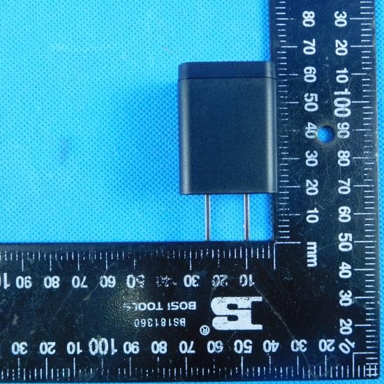
A2HCT9F08
Jun 03, 2021Tablet
Equipment Class
DSS - Part 15 Spread Spectrum Transmitter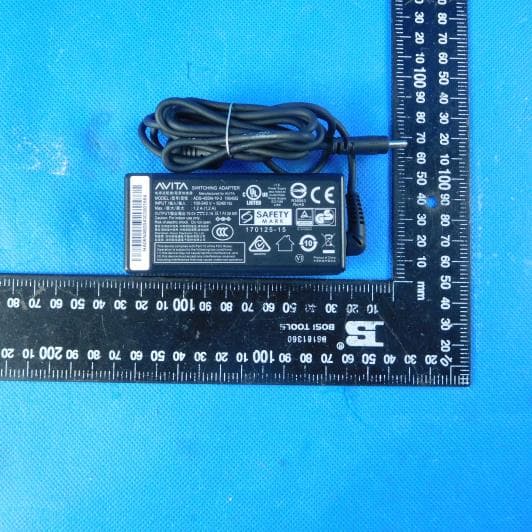
A2HCN6Q15E
Nov 29, 2020Notebook Computer
Equipment Class
DTS - Digital Transmission System
A2HCN6Q15
Oct 27, 2020Notebook Computer
Equipment Class
DTS - Digital Transmission System
A2HRCT6T48
Oct 11, 2020Tablet
Equipment Class
DSS - Part 15 Spread Spectrum Transmitter