A3L5350WLPCI Wireless LAN Card
Samsung Electronics Co Ltd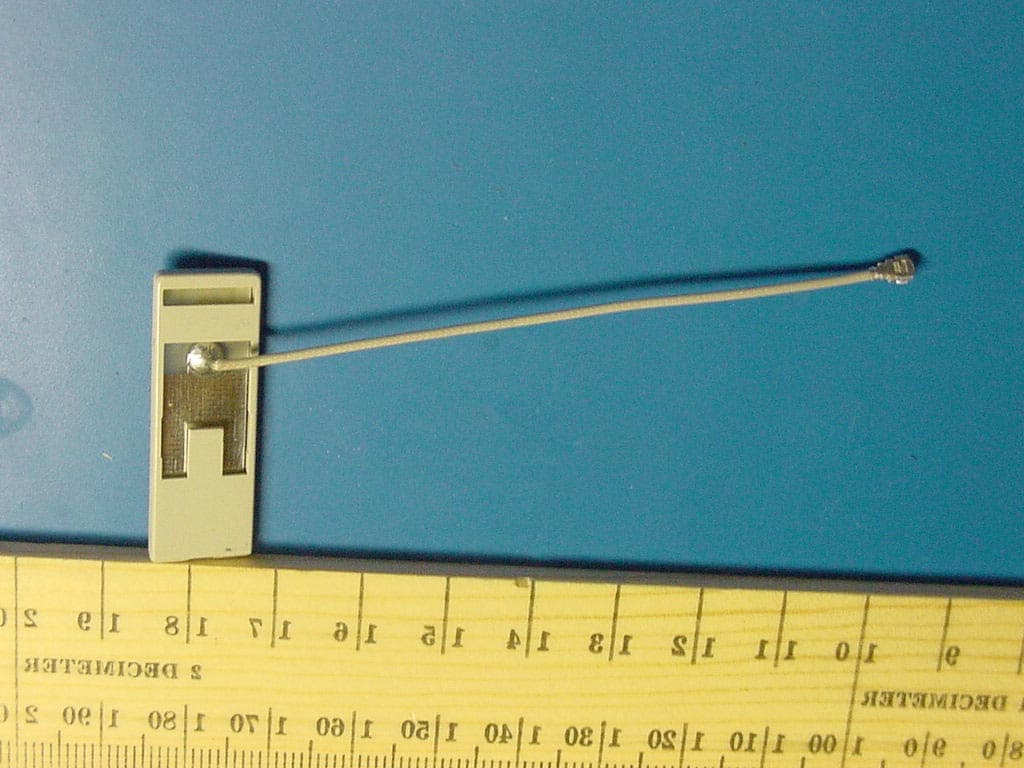
Click to zoom
Application Details
- Equipment Class
- DSS - Part 15 Spread Spectrum Transmitter
- Date of Grant
- Sep 05, 2001
- Application Purpose
- Original Equipment
- Date of Application
- Sep 05, 2001
- Equipment Note
- PCI Wireless LAN Card
- Frequency Range
- 2410.00000000 - 2463.00000000
- Company
- Samsung Electronics Co Ltd
- Country
- United States
Documents & Files
Document Text
Text extracted from the exhibit documents filed with the FCC. Open a document above to read the original.
Users Manual
360 Herndon Parkway Suite 1400 Herndon, VA 20170 http://www.rheintech.com Certification Report Samsung Electronics Page 2 of 67 Document Number: 2001201 FCC ID: A3L535OWL APPENDIX H: MANUAL i Contents 1 Checking Out Your Gateway Solo 5350. . . . . . . . . . . . . . . . . . . . . . . . . . 1 Top . . . . . . . . . . . . . . . . . . . . . . . . . . . . . . . . . . . . . . . . . . . . . . . . . . . . . . . . . . . . . . . 2 Front . . . . . . . . . . . . . . . . . . . . . . . . . . . . . . . . . . . . . . . . . . . . . . . . . . . . . . . . . . . . . 2 Left . . . . . . . . . . . . . . . . . . . . . . . . . . . . . . . . . . . . . . . . . . . . . . . . . . . . . . . . . . . . . . . 3 Right . . . . . . . . . . . . . . . . . . . . . . . . . . . . . . . . . . . . . . . . . . . . . . . . . . . . . . . . . . . . . 3 Back . . . . . . . . . . . . . . . . . . . . . . . . . . . . . . . . . . . . . . . . . . . . . . . . . . . . . . . . . . . . . . 4 Bottom . . . . . . . . . . . . . . . . . . . . . . . . . . . . . . . . . . . . . . . . . . . . . . . . . . . . . . . . . . . . 4 Identifying your model . . . . . . . . . . . . . . . . . . . . . . . . . . . . . . . . . . . . . . . . . . . . . . . . 5 Accessories . . . . . . . . . . . . . . . . . . . . . . . . . . . . . . . . . . . . . . . . . . . . . . . . . . . . . . . . 6 2Getting Started. . . . . . . . . . . . . . . . . . . . . . . . . . . . . . . . . . . . . . . . . . . . . . . . . . . 7 Connecting the AC adapter . . . . . . . . . . . . . . . . . . . . . . . . . . . . . . . . . . . . . . . . . . . . 8 Protecting from power source problems . . . . . . . . . . . . . . . . . . . . . . . . . . . . . . . 9 Starting your notebook . . . . . . . . . . . . . . . . . . . . . . . . . . . . . . . . . . . . . . . . . . . . . . . 9 Waking up your notebook . . . . . . . . . . . . . . . . . . . . . . . . . . . . . . . . . . . . . . . . . . 9 Turning off your notebook . . . . . . . . . . . . . . . . . . . . . . . . . . . . . . . . . . . . . . . . . . . . 10 Using the keyboard . . . . . . . . . . . . . . . . . . . . . . . . . . . . . . . . . . . . . . . . . . . . . . . . . 10 Keys . . . . . . . . . . . . . . . . . . . . . . . . . . . . . . . . . . . . . . . . . . . . . . . . . . . . . . . . . 10 Using the multi-function keys . . . . . . . . . . . . . . . . . . . . . . . . . . . . . . . . . . . . . . . . . 12 Using the EZ Pad touchpad . . . . . . . . . . . . . . . . . . . . . . . . . . . . . . . . . . . . . . . . . . 12 Using the touchpad . . . . . . . . . . . . . . . . . . . . . . . . . . . . . . . . . . . . . . . . . . . . . . 12 Using the rocker switch . . . . . . . . . . . . . . . . . . . . . . . . . . . . . . . . . . . . . . . . . . 13 Connecting the modem . . . . . . . . . . . . . . . . . . . . . . . . . . . . . . . . . . . . . . . . . . . . . . 14 Connecting to an Ethernet network . . . . . . . . . . . . . . . . . . . . . . . . . . . . . . . . . . . . 14 Broadband Internet connections . . . . . . . . . . . . . . . . . . . . . . . . . . . . . . . . . . . . 14 Installing a printer, scanner, or other peripheral device . . . . . . . . . . . . . . . . . . . . . 15 3 Windows Basics . . . . . . . . . . . . . . . . . . . . . . . . . . . . . . . . . . . . . . . . . . . . . . . . 17 About the Windows environment . . . . . . . . . . . . . . . . . . . . . . . . . . . . . . . . . . . . . . 18 Desktop items . . . . . . . . . . . . . . . . . . . . . . . . . . . . . . . . . . . . . . . . . . . . . . . . . . 18 Window items . . . . . . . . . . . . . . . . . . . . . . . . . . . . . . . . . . . . . . . . . . . . . . . . . . 19 Using the Start menu . . . . . . . . . . . . . . . . . . . . . . . . . . . . . . . . . . . . . . . . . . . . . . . 20 Working with files and folders . . . . . . . . . . . . . . . . . . . . . . . . . . . . . . . . . . . . . . . . . 20 About drives . . . . . . . . . . . . . . . . . . . . . . . . . . . . . . . . . . . . . . . . . . . . . . . . . . . 20 About folders and files . . . . . . . . . . . . . . . . . . . . . . . . . . . . . . . . . . . . . . . . . . . 21 Copying and moving files and folders . . . . . . . . . . . . . . . . . . . . . . . . . . . . . . . 21 Deleting files and folders . . . . . . . . . . . . . . . . . . . . . . . . . . . . . . . . . . . . . . . . . 22 Browsing for files and folders . . . . . . . . . . . . . . . . . . . . . . . . . . . . . . . . . . . . . . 23 Searching for files . . . . . . . . . . . . . . . . . . . . . . . . . . . . . . . . . . . . . . . . . . . . . . . . . . 24 ii Using the Windows Me Search utility . . . . . . . . . . . . . . . . . . . . . . . . . . . . . . . .24 Working with documents . . . . . . . . . . . . . . . . . . . . . . . . . . . . . . . . . . . . . . . . . . . . .25 Creating a new document . . . . . . . . . . . . . . . . . . . . . . . . . . . . . . . . . . . . . . . . .25 Saving a document . . . . . . . . . . . . . . . . . . . . . . . . . . . . . . . . . . . . . . . . . . . . . .26 Opening a document . . . . . . . . . . . . . . . . . . . . . . . . . . . . . . . . . . . . . . . . . . . . .26 Printing a document . . . . . . . . . . . . . . . . . . . . . . . . . . . . . . . . . . . . . . . . . . . . . .27 Shortcuts . . . . . . . . . . . . . . . . . . . . . . . . . . . . . . . . . . . . . . . . . . . . . . . . . . . . . .27 Transferring software and hardware from your old computer . . . . . . . . . . . . . . . . .28 Transferring files . . . . . . . . . . . . . . . . . . . . . . . . . . . . . . . . . . . . . . . . . . . . . . . . .28 Transferring Internet settings . . . . . . . . . . . . . . . . . . . . . . . . . . . . . . . . . . . . . . .29 Reinstalling your old printer or scanner . . . . . . . . . . . . . . . . . . . . . . . . . . . . . . .30 Reinstalling your old programs . . . . . . . . . . . . . . . . . . . . . . . . . . . . . . . . . . . . .31 A Safety, Regulatory, and Legal Information. . . . . . . . . . . . . . . . . . . . . . .33 1 1 www.gateway.com Checking Out Yo u r G a t e w ay Solo 5350 Tips & TricksTo ac…
Text truncated - open the document above for the full version.
Cover Letter(s)
Engineering and Testing for EMC and Safety Compliance 360 Herndon Parkway, Suite 1400 Herndon, VA 20170 Phone: 703-689-0368; Fax: 703-689-2056; Metro: 703-471-6441 August 21, 2001 Federal Communications Commission 7435 Oakland Mills Road Columbia, MD 21046 To Whom It May Concern: The following information is to be held confidential pursuant of 47 CFR Part 0 §0.457 and Section 552(b)(4) of the Freedom of Information Act, because the information provided contains trade secrets and proprietary. If made public, the information might be used to the disadvantage of the applicant in the market place. • Schematics • Product Description • Block Diagram • Bill of Materials (Parts List Best Regards, Melissa Carter [email protected] Rhein Tech Laboratories, Inc.
Cover Letter(s)
September 22, 2000 American Telecommunications Certification Body, Inc. 6731 Whittier Avenue Suite C110 McLean, VA 22101 To Whom It May Concern: Please be advised that Samsung authorizes Rhein Tech Laboratories, Inc. to act on our behalf, until otherwise notified, for applications submitted to American Telecommunications Certification Body, Inc. (ATCB). We certify that we are not subject to denial of federal benefits, that includes FCC benefits, pursuant to Section 5301 of the Anti-Drug Abuse ACT of 1988, U.S.C. 862. Further, no party, as defined in 47 CFR 1.2002(b), to the application is subject to denial of federal benefits, that includes FCC benefits. Thank you for your attention to this matter.
Cover Letter(s)
American Telecommunications Certification Body Inc. 6731 Whittier Ave, McLean, VA 22101 August 31, 2001 RE: Samsung Electronics FCC ID: A3L5350WL I have some confusion with regards to this Application which must be resolved. 1. External Photographs show only an antenna; Internal Photographs a PCI card; and Label photograph shows a notebook computer. How are all these items related? If this Application will relate only to this specific setup, then a Grant restriction will indicate this device will be allowed in FCC ID: A3L5350015318 notebook computer only Please place restriction for this notebook only. The manufacturer to sell as a system will place this device inside the notebook. Therefore, the label that is visible to the public must indicate the FCC ID of the WLAN is inside the PC. Please note: that there are 2 antennas inside the notebook. Both antennas are the same. The object of having 2 antennas is that while one is transmitting the other can receive. 2. Are you seeking modular approval on this PCI card? If not, the Grant will allow this device only within this specific notebook computer. If modular approval is indeed requested, retesting will have to be performed on an extender card of some sort to get the transceiver outside of the computer case. Product Description indicates approval is being sought on mini PCI wireless LAN card only, which sounds a lot like a modular approval request. We are not seeking a modular approval on this device. 3. Table 8-1 of the test report indicates a negative gain antenna. RF Exposure uses a +1dBi gain antenna, Antenna spec uses unity gain. Please correct discrepancies. Please see the revised RF exposure information. 4. FYI: In the future I will be requiring a limit line set at 500uV when showing Restricted Band Edge data in addition to the tabular data found in Section 13. Noted. 5. Agent Authorization letter missing. The letter has been uploaded. Please note that the Processing Gain has also been uploaded for your review. William H. Graff Examining Engineer President and Director of Engineering mailto:[email protected] The items indicated above must be submitted before processing can continue on the above referenced application. Failure to provide the requested information may result in application termination. Correspondence should be considered part of the permanent submission and may be viewed from the Internet after a Grant of Equipment Authorization is issued. Please do not respond to this correspondence using the email reply button. In order for your response to be processed expeditiously, you must submit your documents through the AmericanTCB.com website. Also, please note that partial responses increase processing time and should not be submitted. Any questions about the content of this correspondence should be directed to the sender.
Cover Letter(s)
American Telecommunications Certification Body Inc. 6731 Whittier Ave, McLean, VA 22101 August 31, 2001 RE: Samsung Electronics FCC ID: A3L5350WL I have some confusion with regards to this Application which must be resolved. 1.) External Photographs show only an antenna; Internal Photographs a PCI card; and Label photograph shows a notebook computer. How are all these items related? If this Application will relate only to this specific setup, then a Grant restriction will indicate this device will be allowed in FCC ID: A3L5350015318 notebook computer only 2.) Are you seeking modular approval on this PCI card? If not, the Grant will allow this device only within this specific notebook computer. If modular approval is indeed requested, retesting will have to be performed on an extender card of some sort to get the transceiver outside of the computer case. Product Description indicates approval is being sought on mini PCI wireless LAN card only, which sounds a lot like a modular approval request. 3.) Table 8-1 of the test report indicates a negative gain antenna. RF Exposure uses a +1dBi gain antenna, Antenna spec uses unity gain. Please correct discrepancies. 4.) FYI: In the future I will be requiring a limit line set at 500uV when showing Restricted Band Edge data in addition to the tabular data found in Section 13. 5.) Agent Authorization letter missing. William H. Graff Examining Engineer President and Director of Engineering mailto:[email protected] The items indicated above must be submitted before processing can continue on the above referenced application. Failure to provide the requested information may result in application termination. Correspondence should be considered part of the permanent submission and may be viewed from the Internet after a Grant of Equipment Authorization is issued. Please do not respond to this correspondence using the email reply button. In order for your response to be processed expeditiously, you must submit your documents through the AmericanTCB.com website. Also, please note that partial responses increase processing time and should not be submitted. Any questions about the content of this correspondence should be directed to the sender.
External Photos
360 Herndon Parkway Suite 1400 Herndon, VA 20170 http://www.rheintech.com Certification Report Samsung Electronics Page 9 of 67 Document Number: 2001201 FCC ID: A3L535OWL APPENDIX K: ANTENNA PHOTOGRAPHS PHOTOGRAPH 13-9: WLAN ANTENNA TOP 360 Herndon Parkway Suite 1400 Herndon, VA 20170 http://www.rheintech.com Certification Report Samsung Electronics Page 10 of 67 Document Number: 2001201 FCC ID: A3L535OWL PHOTOGRAPH 13-10: WLAN ANTENNA BOTTOM 360 Herndon Parkway Suite 1400 Herndon, VA 20170 http://www.rheintech.com Certification Report Samsung Electronics Page 11 of 67 Document Number: 2001201 FCC ID: A3L535OWL PHOTOGRAPH 13-11: CONNECTOR WLAN ANT
ID Label/Location Info
360 Herndon Parkway Suite 1400 Herndon, VA 20170 http://www.rheintech.com Certification Report Samsung Electronics Page 42 of 67 Document Number: 2001201 FCC ID: A3L535OWL APPENDIX D: LABEL INFORMATION Warning Label FCC ID Label Location This device complies with part 15 of the FCC Rules. Operation is subject to the following two conditions: 1) This device may not cause harmful interference, and 2) this device must accept any interference received, including interference that may cause undesired operation. This device contains inside FCC ID: A3L535OWL CANADA 210: XXXXXXXXX Label Location
Internal Photos
360 Herndon Parkway Suite 1400 Herndon, VA 20170 http://www.rheintech.com Certification Report Samsung Electronics Page 5 of 67 Document Number: 2001201 FCC ID: A3L535OWL APPENDIX J: INTERNAL PHOTOGRAPHS PHOTOGRAPH 13-5: TOP VIEW 360 Herndon Parkway Suite 1400 Herndon, VA 20170 http://www.rheintech.com Certification Report Samsung Electronics Page 6 of 67 Document Number: 2001201 FCC ID: A3L535OWL PHOTOGRAPH 13-6: BOTTOM VIEW 360 Herndon Parkway Suite 1400 Herndon, VA 20170 http://www.rheintech.com Certification Report Samsung Electronics Page 7 of 67 Document Number: 2001201 FCC ID: A3L535OWL PHOTOGRAPH 13-7: TOP VIEW OF THE BOARD WITHOUT CAN 360 Herndon Parkway Suite 1400 Herndon, VA 20170 http://www.rheintech.com Certification Report Samsung Electronics Page 8 of 67 Document Number: 2001201 FCC ID: A3L535OWL PHOTOGRAPH 13-8: BOTTOM VIEW OF THE BOARD WITHOUT CAN
RF Exposure Info
360 Herndon Parkway Suite 1400 Herndon, VA 20170 http://www.rheintech.com Certification Report Samsung Electronics Page 35 of 67 Document Number: 2001201 FCC ID: A3L535OWL APPENDIX C: ANTENNA SPECIFICATIONS 360 Herndon Parkway Suite 1400 Herndon, VA 20170 http://www.rheintech.com Certification Report Samsung Electronics Page 36 of 67 Document Number: 2001201 FCC ID: A3L535OWL 360 Herndon Parkway Suite 1400 Herndon, VA 20170 http://www.rheintech.com Certification Report Samsung Electronics Page 37 of 67 Document Number: 2001201 FCC ID: A3L535OWL 360 Herndon Parkway Suite 1400 Herndon, VA 20170 http://www.rheintech.com Certification Report Samsung Electronics Page 38 of 67 Document Number: 2001201 FCC ID: A3L535OWL 360 Herndon Parkway Suite 1400 Herndon, VA 20170 http://www.rheintech.com Certification Report Samsung Electronics Page 39 of 67 Document Number: 2001201 FCC ID: A3L535OWL 360 Herndon Parkway Suite 1400 Herndon, VA 20170 http://www.rheintech.com Certification Report Samsung Electronics Page 40 of 67 Document Number: 2001201 FCC ID: A3L535OWL 360 Herndon Parkway Suite 1400 Herndon, VA 20170 http://www.rheintech.com Certification Report Samsung Electronics Page 41 of 67 Document Number: 2001201 FCC ID: A3L535OWL
Test Report
Engineering and Testing for EMC and Safety Compliance 360 Herndon Parkway, Suite 1400 Herndon, VA 20170 Phone: 703-689-0368; Fax: 703-689-2056; Metro: 703-471-6441 APPLICATION FOR FCC CERTIFICATION DIRECT SEQUENCE SPREAD SPECTRUM TRANSMITTER Samsung Electronics 416, Maetan-3Dong,Paldal-Gu Suwon City, Kyunggi-Do, Korea, 442-743 +82-31-200-7925 Model: Wireless LAN Card (Solo 5350) FCC ID: A3L5350WL July 30, 2001 S TANDARDS R EFERENCED FOR THIS R EPORT P ART 2: 1999 F REQUENCY A LLOCATIONS AND R ADIO T REATY M ATTERS ; G ENERAL R ULES AND R EGULATIONS P ART 15: 1999 R ADIO F REQUENCY D EVICES FCC 97-114 G UIDANCE ON M EASUREMENTS FOR D IRECT S EQUENCE S PREAD S PECTRUM S YSTEMS ANSI C63.4-1992 S TANDARD F ORMAT M EASUREMENT /T ECHNICAL R EPORT P ERSONAL C OMPUTER AND P ERIPHERALS RSS-210; I SSUE 5 (D RAFT 3) L OW P OWER L ICENCE -E XEMPT R ADIOCOMMUNICATION D EVICES (A LL F REQUENCY B ANDS RSS-102; I SSUE 1 (P ROVISIONAL ) E VALUATION P ROCEDURE FOR M OBILE AND P ORTABLE R ADIO T RANSMITTERS WITH RESPECT TO H EALTH C ANADA ’ S S AFETY C ODE 6 FOR E XPOSURE OF H UMANS TO R ADIO F REQUENCY F IELDS Frequency Range Conducted Output Power (W) Freq. Tolerance Emission Designator 2410 to 2463 MHz 0.031 REPORT PREPARED BY: EMC Engineer: Rachid Sehb Supervising Engineer: Bruno Clavier Document Number: 2001201 / QRTL01-196 No part of this report may be reproduced without the full written approval of Rhein Tech Laboratories, Inc. 360 Herndon Parkway Suite 1400 Herndon, VA 20170 http://www.rheintech.com Certification Report Samsung Electronics Page 2 of 67 Document Number: 2001201 FCC ID: A3L535OWL TABLE OF CONTENTS 1 INTRODUCTION ......................................................................................................................................................................................4 1.1 RELATED SUBMITTAL (S)/GRANT (S) .......................................................................................................................................................................4 1.2 TEST METHODOLOGY .................................................................................................................................................................................................4 1.3 TEST FACILITY..............................................................................................................................................................................................................4 2 SYSTEM TEST CONFIGURATION .........................................................................................................................................................5 2.1 JUSTIFICATION.............................................................................................................................................................................................................5 2.2 EUT EXERCISE SOFTWARE........................................................................................................................................................................................5 2.3 SPECIAL ACCESSORIES .............................................................................................................................................................................................5 2.4 TEST SYSTEM DETAILS ..............................................................................................................................................................................................5 2.5 CONFIGURATION OF TESTED SYSTEM ....................................................................................................................................................................6 3 CONFORMANCE STATEMENT..............................................................................................................................................................7 4 FIELD STRENGTH CALCULATION .......................................................................................................................................................8 5 CONDUCTED EMISSIONS MEASUREMENTS......................................................................................................................................9 5.1 CONDUCTED EMISSIONS TEST .................................................................................................................................................................................9 5.1.1 FCC PART 15 §15.107 CONDUCTED EMISSIONS TEST DATA...................................................................................................................................10 6 FCC PART 15 §15.109 RADIATED EMISSIONS MEASUREMENTS..................................................................................................11 6.1 FCC PART 15 §15.109 RADIATED EMISSIONS TEST .............................................................................................................................................12 6.1.1 FCC PART 15 §15.109 RADIATED EMISSION DIGITAL NOISE......................................................................................................................................12 7 FCC PART 15 §15.247(A)(2) MODULATED BANDWIDTH .................................................................................................................13 8 FCC PART 15 §15.247(B) POWER OUTPUT.......................................................................................................................................17 9 FCC PART 15 §15.247(C) ANTENNA CONDUCTED SPURIOUS EMISSIONS..................................................................................18 10 FCC PART 15 §15.209(C) RADIATED SPURIOUS EMISSIONS.........................................................................................................21 11 FCC PART 15 §15.247(D) POWER SPECTRAL DENSITY .............................................................................................................…
Text truncated - open the document above for the full version.
Test Report
Nederland B.V. WCND Report No. 015127, Rev. A TEST REPORT Subject: Processing Gain For the ORiNOCO IEEE802.11b products Ref.: FCC Rules 47 CFR Part 15, Section 5.247d Report Prepared by: Maarten Visee July 28, 2000 NameSignatureDate Concurrence: 1. Director of Engineering Bruce Tuch August 10, 2000 NameSignatureDate 2. Team Captain Frans Hoekstra August 10, 2000 NameSignatureDate Lucent WCND Confidential Information ©2000 FCC Processing Gain Measurements Results, Report No. 015127, Rev. A. Lucent WCND Confidential ©2000 i Date SectionDescription 07/28/00, Rev. A Initial release. 0Change History: FCC Processing Gain Measurements Results, Report No. 015127, Rev. A. Lucent WCND Confidential ©2000 1 This document describes the Receiver Processing Gain verification measurements performed at the Lucent Technologies ORiNOCO IEEE802.11b products according to Ref.[2] and Ref.[5]. The Lucent Technologies ORiNOCO Mini PCI product conforms to the minimum required 10 dB processing gain, as set forth by the FCC for operation in the 2.4 GHz ISM band. 1- Document FCC 97-114, Appendix C, Guidance on Measurements for Direct Sequence Spread Spectrum Systems. 2- Hardware Functional Specification for WaveLAN-II Embedded, High Speed, Doc. No. 011735, Rev. A, Source Organization Lucent Technologies WCND Utrecht. 3-Viterbi, A. J., Principles of Coherent Communications, New York, McGraw-Hill 1966. 4- Proakis, J.G., Digital Communications, New York, McGraw-Hill 1989, page 270. 5- Hardware Functional Specification for the Lucent Technologies ORiNOCO Mini PCI, Doc. No. 015143, Source Organization Lucent Technologies WCND Utrecht. 4.1 Test introduction - FCC requirements: Part of FCC certification for Lucent Technologies ORiNOCO IEEE802.11b High Speed compliant Network Interface Cards (NIC) is a processing gain test. This test proves that the receiver of the tested product employs a true spread spectrum device receiver structure, taking full advantage of the direct sequence spread spectrum modulation technique. This test verifies the receiver processing gain to be 10 dB or more for a data rate of 1, 2, 5.5 and 11 Mbit/s, by monitoring the Bit Error Rate (BER) of the product under test for each data rate, while operating under strict defined received signal conditions. Several methods of showing compliance to the rules are possible, from a stepped CW jammer to a continuous sweeping CW interferer. For this test the discrete stepped CW jammer method was chosen, as described in Ref.[1]. 1.Summary: 2.Conclusion: 3.References: 4.Measurement description: FCC Processing Gain Measurements Results, Report No. 015127, Rev. A. Lucent WCND Confidential ©2000 2 Therefore a receiver input signal is applied to the product under test, in the presence of a Continuous Wave (CW) interference source, also referred to as CW jammer. The test takes place at the product Functional Specification (Ref.[2], Ref.[5]) specified conditions for BER rate measurements, specifying a BER equal or better than 10^-8 at a receiver input level of -55 dBm. For practical reasons these test are performed at -55 dBm or -53 dBm. This small deviation from the Functional Specification should not cause any deviation from the specified Bit Error Rate, since the received levels are well above the thermal noise. The test criteria for meeting the minimal processing gain is such that it takes the theoretical calculated SNR for the applied modulation technique and specified BER as a reference. From this given SNR the processing gain is subtracted, yielding the CW Jammer to Signal ratio J/S. From Ref. [4], likewise as Ref.[3] consulted in Ref. [1], it is determined that for a BER of 10^-8 the SNR (S/N)o equals: 13 dB @ 1 Mbit/s, 15 dB @ 2 Mbit/s, 15 dB @ 5.5 Mbit/s, 18 dB @ 11 Mbit/s. Thus the J/S ratio for a processing gain of 10 dB that must be met is calculated as: -13 + 10 = -3 dB @ 1 Mbit/s (DBPSK), -15 + 10 = -5 dB @ 2 Mbit/s (DQPSK), -15 + 10 = -5 dB @ 5.5 Mbit/s (CCK), -18 + 10 = -8 dB @ 11 Mbit/s (CCK). Two types of measurement corrections are allowed for as described in Ref.[1]. The first taking into account 2 dB implementation losses, thus increasing the absolute J/S ratio by 2 dB. The second correction allows for deleting the 20% worst- case frequencies in the processing gain test that causes the test at that CW interference to fail. This implies that for the considered 14 MHz wide measurement interval the worst case 57 CW jammer frequencies can be ignored, being those that result in received data errors/missing frames (20% of 14 MHz *(1 MHz/50 KHz) + 1 = (20% * 281) + 1 = 57). FCC Processing Gain Measurements Results, Report No. 015127, Rev. A. Lucent WCND Confidential ©2000 3 4.2 Test sequence: The measurements are performed at a 50 KHz CW jammer raster. For each CW jammer frequency 10^8 bits are transmitted by the reference transmitter, and received by the product under test. For practical reasons 50.000 messages are transmitted. After blanking out frame overhead 1927 bits per frame are monitored. This results in 50.000 * 1927 = 9650000 transmitted bits for a BER test, which is a mere 1.4% less than the targeted 10^8 bits. Though it would be more elegant to show BER compliance for at least say ten times 10^8 transmitted/received bits, the time involved with this grows significantly. Since the CW interferer is stepped in a 50 KHz raster, covering the receiver bandwidth of 14 MHz, it is considered that the BER requirement is sufficiently met since such a multitude of measurements are taken. The total measurement is being performed under computer control, hereafter referred to as controller. It involves the control over the reference transmitter, CW-interference generator, receiver under test and received data error- checker/frame counter. The controller is programmed by a configuration file, that lists the CW jammer frequencies and CW jammer signal levels. The controller program flow chart is given in Annex A, WaveLAN-II FCC Processing Gain Measurements, Co…
Text truncated - open the document above for the full version.
Test Setup Photos
360 Herndon Parkway Suite 1400 Herndon, VA 20170 http://www.rheintech.com Certification Report Samsung Electronics Page 3 of 67 Document Number: 2001201 FCC ID: A3L535OWL APPENDIX I: TEST PHOTOGRAPHS PHOTOGRAPH 13-1: CONDUCTED EMISSIONS FRONT VIEW PHOTOGRAPH 13-2: CONDUCTED EMISSIONS REAR VIEW 360 Herndon Parkway Suite 1400 Herndon, VA 20170 http://www.rheintech.com Certification Report Samsung Electronics Page 4 of 67 Document Number: 2001201 FCC ID: A3L535OWL Radiated Measurement Photos PHOTOGRAPH 13-3: RADIATED EMISSIONS FRONT VIEW PHOTOGRAPH 13-4: RADIATED EMISSIONS REAR VIEW
Contact Information
Applicant
Jenni Chun(General Manager)
Technical Contact
Rhein Tech Laboratories, Inc.Rachid Sehb
[email protected]703 689 0368
360 Herndon Parkway · Herndon, Virginia · United States
Test Firm
Rhein Tech Laboratories, Inc.Rick McMurray
Technical Specifications
| # | Rule Parts | Frequency Range | Power Output |
|---|---|---|---|
| 1 | 15C | 2.41 GHz - 2.46 GHz | 31.00 mW |
Other Applications from Samsung Electronics Co Ltd
A3LSMS741B
Aug 05, 2026Portable Handset
Equipment Class
6VL - 15E 6 GHZ Very Low Power DeviceA3LSMX940
Jul 31, 2026BT,BLE Tablet DTS,UNII a,b,g,n,ac,ax,be and digitizer
Equipment Class
DTS - Digital Transmission SystemA3LSMS741U
Jul 30, 2026Portable Handset
Equipment Class
6CD - 15E 6 GHz Low Power Dual ClientA3LSMX840
Jul 27, 2026BT,BLE Tablet DTS,UNII a,b,g,n,ac,ax and Digitizer
Equipment Class
DSS - Part 15 Spread Spectrum TransmitterA3LSMX848U
Jul 27, 2026WCDMA, LTE, 5G NR Tablet BT,BLE, DTS,UNII a b g n ac ax and Digitizer
Equipment Class
JBP - Part 15 Class B Computing Device Peripheral