A7V20102201Dual Band Wireless Cell Phone Signal Amplifier
ShenZhen SolidRF Communications Co., Ltd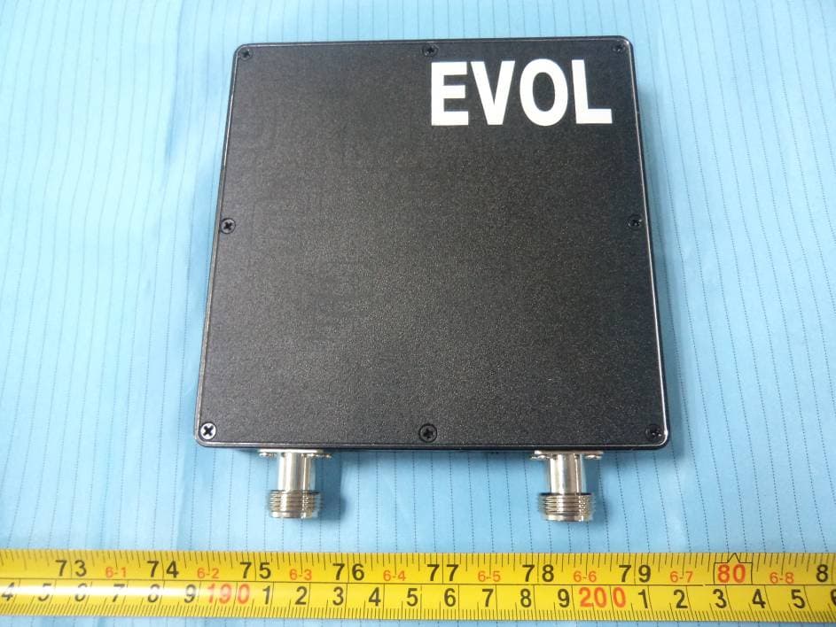
Click to zoom
Application Details
- Equipment Class
- PCB - PCS Licensed Transmitter
- Date of Grant
- Mar 01, 2012
- Application Purpose
- Original Equipment
- Date of Application
- Mar 01, 2012
- Equipment Note
- Dual Band Wireless Cell Phone Signal Amplifier
- Frequency Range
- 1932.40000000 - 1987.60000000
- Country
- China
Documents & Files
Document Text
Text extracted from the exhibit documents filed with the FCC. Open a document above to read the original.
Users Manual
1 2 Contents 1Introduction................................................................................................................................................. 3 1.1 Application background........................................................................................................................... 3 2 System (the) introduction................................................................................................................................... 4 2.1 System composition and principle block diagram in the paper......................................................... 4 2.1.1 Diagram of the system of the..................................................................................................... 4 2.1.2 System principle outlined............................................................................................................ 4 2.2 The composition and principle block diagram in the paper............................................................... 5 2.2.1 The block diagram of................................................................................................................... 5 ................................................................................................................................................................... 5 2.2.2 The principles outlined................................................................................................................ 5 3Function.................................................................................................................................................................. 6 3.1.1 Rf index.................................................................................................................................................. 6 3.2 structure.................................................................................................................................................... 7 3.2.1 cooling............................................................................................................................................ 7 3.2.2 appearance.................................................................................................................................... 7 3.2.3 installation.................................................................................................................................... 7 3.2.4 Interface and function is introduced......................................................................................... 7 4 performance.......................................................................................................................................................... 8 4.1 environment.............................................................................................................................................. 8 3 We declare that: ※ the product is installed with battery separately in the box. The FCC ID label is placed on Mobile Payment Terminal clearly visible to all persons at the time of purchase. ※ the user is cautioned that changes or modifications not expressly approved by the manufacturer could void the user’s authority to operate the equipment. ※ This device complies with part 15 of the FCC Rules. Operation is subject to the following two conditions: (1) This device may not cause harmful interference, and (2) This device must accept any interference received, including interference that may cause undesired operation. ※ Do not attempt to disassemble the Mobile Payment Terminal and battery by yourself. Non-expert handling of the devices may damage them. ※Any Changes or modifications not expressly approved by the party responsible for compliance could void the user's authority to operate the equipment ※FCC Radiation Exposure Statement: To comply with FCC RF exposure requirements in section 1.1307, a minimum separation distance of 20 cm is required between the antenna and all occupational persons, and a minimum separation distance of 20 cm is required between the antenna and all public persons. This device complies with Industry Canada licence-exempt RSS standard(s). Operation is subject to the following two conditions: (1) this device may not cause interference, and (2) this device must accept any interference, including interference that may cause undesired operation of the device. It was required to meet requirement of RSS-Gen Section 7.1.3. 1 Introduction 1.1 Application background Due to the mobile communication network covers not perfect, the remote suburbs highway, cell phone signal existence covered blind spots. Residents drove go out, mobile phone often appear weak signal, the phenomenon such as no signal. In order to solve the problem, the residents used to buying their own cell phone signal amplifier products, local area signal coverage, in order to meet the communication needs. 4 2 System (the) introduction 2.1 System composition and principle block diagram in the paper 2.1.1 Diagram of the system of the Cell phone signal amplifier communication schemes 2.1.2 System principle outlined 1. This product is suitable for WCDMA、CDMA and GSM type of network。 2. Cell phone signal amplifier (and amplifier for synonyms hereinafter referred to as the amplifier), amplifiers, feeder, antenna etc。 3. The amplifier's working principle is descending amplifier through the installation in the OUTDOOR antenna base station downline weak signal, and then through the rf feeder will signal is introduced into equipment. Amplifier to the introduction of the weak base station downside signal filter and amplification, and through the INDOOR antenna will enlarge the signal after launch out to meet demand cover 。 4. Uplink working principle: the amplifier INDOOR antenna to mobile terminal of the uplink signal, through the rf feeder introduced to the equipment. Equipment will be up for filter and amplification signal, and then through the rf feeder connected to the OUTDO…
Text truncated - open the document above for the full version.
External Photos
EXHIBIT B - EUT EXTERNAL PHOTOGRAPHS EUT – With AC/DC Adapter View EUT – Top View EUT – Bottom View EUT – Front View EUT – Side View
ID Label/Location Info
EXHIBIT A - FCC ID LABELING AND LOCATION FCC ID Label Proposed FCC ID Label Location The label shown shall be permanently affixed at a conspicuous location on the device and be readily visible to the user at the time purchase (Labeling requirements per 2.925) Label Here
Internal Photos
EXHIBIT C - EUT INTERNAL PHOTOGRAPHS EUT – Cover off View EUT – Top Shielding off View EUT – Bottom Shielding off View EUT –Main Board Top View EUT –Main Board Bottom View EUT – Adapter View EUT – Adapter Label View
Test Report
Note: This test report is prepared for the customer shown above and for the device described herein. It may not be duplicated or used in part without prior written consent from Bay Area Compliance Laboratories Corp. This report must not be used by the customer to claim product certification, approval, or endorsement by NVLAP*, or any agency of the Federal Government. * This report may contain data that are not covered by the NVLAP accreditation and are marked with an asterisk “★” (Rev.2) FCC PART 22H, 24E MEASUREMENT AND TEST REPORT For ShenZhen EVOL Technology Development Co., Ltd No. 8 Shop D, Block C Shan Shui Ju, Long Wei Road, Futian District, Shenzhen, Guangdong, China FCC ID: A7V20102201 Report Type: Original Report Product Type: Dual Band Wireless Cell Phone Signal Amplifier Test Engineer: Henry Ding Report Number: RSZ111209001-00 Report Date: 2012-03-02 Reviewed By: Alvin Huang EMC Engineer Test Laboratory: Bay Area Compliance Laboratories Corp. (Shenzhen) 6/F, the 3rd Phase of WanLi Industrial Building, ShiHua Road, FuTian Free Trade Zone Shenzhen, Guangdong, China Tel: +86-755-33320018 Fax: +86-755-33320008 www.baclcorp.com.cn Bay Area Compliance Laboratories Corp. (Shenzhen) Report No.: RSZ111209001-00 FCC Part 22H/24E Page 2 of 140 TABLE OF CONTENTS GENERAL INFORMATION.......................................................................................................................................3 PRODUCT DESCRIPTION FOR EQUIPMENT UNDER TEST (EUT) .....................................................................................3 OBJECTIVE...................................................................................................................................................................3 RELATED SUBMITTAL(S)/GRANT(S).............................................................................................................................3 TEST METHODOLOGY..................................................................................................................................................3 TEST FACILITY.............................................................................................................................................................4 SYSTEM TEST CONFIGURATION ..........................................................................................................................5 JUSTIFICATION.............................................................................................................................................................5 EQUIPMENT MODIFICATIONS.......................................................................................................................................5 SUPPORT EQUIPMENT LIST AND DETAILS....................................................................................................................5 EXTERNAL I/O CABLE..................................................................................................................................................5 CONFIGURATION OF TEST SETUP.................................................................................................................................6 BLOCK DIAGRAM OF TEST SETUP................................................................................................................................6 SUMMARY OF TEST RESULTS...............................................................................................................................7 FCC §1.1307 & §2.1091- MAXIMUM PERMISSIBLE EXPOSURE (MPE).............................................................8 APPLICABLE STANDARD..............................................................................................................................................8 TEST DATA..................................................................................................................................................................8 FCC §2.1047 - MODULATION CHARACTERISTIC ............................................................................................10 FCC § 2.1046, § 22.913(A), § 24.232(C) - RF OUTPUT POWER ...........................................................................11 APPLICABLE STANDARD............................................................................................................................................11 TEST PROCEDURE......................................................................................................................................................11 TEST EQUIPMENT LIST AND DETAILS.........................................................................................................................11 TEST DATA................................................................................................................................................................12 FCC §2.1049, §22.917, §22.905& §24.238 - OCCUPIED BANDWIDTH ...............................................................40 APPLICABLE STANDARDS...........................................................................................................................................40 TEST PROCEDURE......................................................................................................................................................40 TEST EQUIPMENT LIST AND DETAILS.........................................................................................................................40 TEST DATA................................................................................................................................................................40 FCC §2.1051, §22.917(A) &§24.238(A) - SPURIOUS EMISSIONS AT ANTENNA TERMINALS ...................77 APPLICABLE STANDARDS...........................................................................................................................................77 TEST PROCEDURE..................................................…
Text truncated - open the document above for the full version.
Test Setup Photos
EXHIBIT D - TEST SETUP PHOTOGRAPHS Radiated Emissions View
Contact Information
Applicant
Yu Chi(CEO)
Test Firm
Bay Area Compliance Laboratory Corp. (Shenzhen)John Chan
Technical Specifications
| # | Rule Parts | Frequency Range | Power Output | Emission | Tolerance |
|---|---|---|---|---|---|
| 15 | 24E | 1.93 GHz - 1.99 GHz | 11.00 mW | F9W | Amp |
Other Applications from ShenZhen SolidRF Communications Co., Ltd
A7V-SR15652001
Jul 30, 2021Signal Booster
Equipment Class
B2W - Part 20 Wideband Consumer Booster (CMRS)
A7V-SR55652001
Jul 20, 2021Signal Booster
Equipment Class
B2W - Part 20 Wideband Consumer Booster (CMRS)
A7V-SR87503001
Jan 05, 2020Signal Booster
Equipment Class
B2W - Part 20 Wideband Consumer Booster (CMRS)
A7V-SR25502001
Mar 02, 2015Mobile Consumer Booster
Equipment Class
B2W - Part 20 Wideband Consumer Booster (CMRS)
A7V-SR25652001
Feb 11, 20155 band consumer signal booster for home use
Equipment Class
B2W - Part 20 Wideband Consumer Booster (CMRS)