AEZSCP-4920Tri-Mode Dual-Band Analog/ PCS Phone (AMPS/ CDMA)
Sanyo Electric Co Ltd
Click to zoom
Application Details
- Equipment Class
- PCE - PCS Licensed Transmitter held to ear
- Date of Grant
- Apr 14, 2004
- Application Purpose
- Original Equipment
- Date of Application
- Apr 14, 2004
- Equipment Note
- Tri-Mode Dual-Band Analog/ PCS Phone (AMPS/ CDMA)
- Frequency Range
- 1851.25000000 - 1908.75000000
- Company
- Sanyo Electric Co Ltd
- Country
- United States
Documents & Files
Document Text
Text extracted from the exhibit documents filed with the FCC. Open a document above to read the original.
Cover Letter(s)
February 25, 2004 Federal Communications Commission Equipment Approval Services 7435 Oakland Mills Road Columbia, MD 21046 SUBJECT: SANYO ELECTRIC Co., Ltd. FCC ID: AEZSCP-4920 Part 22/24 Certification Gentlemen: Submitted herewith, on behalf of SANYO ELECTRIC Co., Ltd., is an application for Part 22/ 24 Certification of the Tri-Mode Dual-Band Analog/ PCS phone. Attached is the applicant’s Letter of Authorization, Confidentiality Request, E911 Affidavit, measurement report test data and plots, RF Exposure measurement report and data, FCC ID label and location, test setup photographs, internal and external photographs, block diagram (confidential), circuit diagrams & description (confidential), operational description (confidential), parts list & tune-up procedure (confidential), and the user's manual. Should you have any questions or comments concerning the above, please contact the undersigned. cc: SANYO ELECTRIC Co., Ltd.
External Photos
SANYO FCC ID: AEZSCP-4920 EUT Photographs © 2004 PCTEST Lab. Tri-Mode Dual-Band Analog/PCS Phone Model: SCP-4920 SANYO FCC ID: AEZSCP-4920 EUT Photographs © 2004 PCTEST Lab. Tri-Mode Dual-Band Analog/PCS Phone Model: SCP-4920 SANYO FCC ID: AEZSCP-4920 EUT Photographs © 2004 PCTEST Lab. Tri-Mode Dual-Band Analog/PCS Phone Model: SCP-4920 SANYO FCC ID: AEZSCP-4920 EUT Photographs © 2004 PCTEST Lab. Tri-Mode Dual-Band Analog/PCS Phone Model: SCP-4920 SANYO FCC ID: AEZSCP-4920 EUT Photographs © 2004 PCTEST Lab. Tri-Mode Dual-Band Analog/PCS Phone Model: SCP-4920 SANYO FCC ID: AEZSCP-4920 EUT Photographs © 2004 PCTEST Lab. Tri-Mode Dual-Band Analog/PCS Phone Model: SCP-4920
ID Label/Location Info
PCTEST PT. 22/24 REPORT FCC CERTIFICATION Reviewed By: Quality Manager Test Report S/N: 22/24.240209132.AEZ Test Dates: February 9-12, 2004 EUT Type: Tri-Mode Dual-Band Phone FCC ID: AEZSCP-4920 Page 1 of 1 FCC ID SAMPLE LABEL & LOCATION LABELLING REQUIREMENTS The Label shown shall be permanently affixed at a conspicuous location on the device and be readily visible to the user at the time of purchase. (SEE NEXT PAGE)
Internal Photos
SANYO FCC ID: AEZSCP-4920 EUT Photographs © 2004 PCTEST Lab. Tri-Mode Dual-Band Analog/PCS Phone Model: SCP-4920 SANYO FCC ID: AEZSCP-4920 EUT Photographs © 2004 PCTEST Lab. Tri-Mode Dual-Band Analog/PCS Phone Model: SCP-4920 SANYO FCC ID: AEZSCP-4920 EUT Photographs © 2004 PCTEST Lab. Tri-Mode Dual-Band Analog/PCS Phone Model: SCP-4920 SANYO FCC ID: AEZSCP-4920 EUT Photographs © 2004 PCTEST Lab. Tri-Mode Dual-Band Analog/PCS Phone Model: SCP-4920 SANYO FCC ID: AEZSCP-4920 EUT Photographs © 2004 PCTEST Lab. Tri-Mode Dual-Band Analog/PCS Phone Model: SCP-4920 SANYO FCC ID: AEZSCP-4920 EUT Photographs © 2004 PCTEST Lab. Tri-Mode Dual-Band Analog/PCS Phone Model: SCP-4920 SANYO FCC ID: AEZSCP-4920 EUT Photographs © 2004 PCTEST Lab. Tri-Mode Dual-Band Analog/PCS Phone Model: SCP-4920 SANYO FCC ID: AEZSCP-4920 EUT Photographs © 2004 PCTEST Lab. Tri-Mode Dual-Band Analog/PCS Phone Model: SCP-4920
Operational Description
Applicant: SANYO Electric CO., LTD. Transmitter Type: AEZSCP-4920 EXHIBIT xx 1 / 5 TECHNICAL DESCRIPTION This transmitter has been specially designed for the Domestic Personal Communication Service (PCS band CDMA) and the Domestic Cellular Radiotelephone Communication Service (Cellular band AMPS/CDMA). [PCS band CDMA ] The rated maximum power output for CDMA is 0.5 watts with the capability of reducing the maximum power in a step of 1 dB on command from the base station. The transmitter output is confirmed correspond to the received power level of the mobile station. Each power level is maintained within +2 /-4 dB of its nominal level over the temperature range from –30 to +60 degrees centigrade and +14 –14% change of the supply voltage. This transmitter operates in the frequency range of 1851.250 MHz to 1908.250 MHz. The frequencies are generated by Phase Locked Loop Frequency Synthesizers, which are controlled by the closest base station in the system. The handset causes the frequency stability of carrier according to the frequency from the base station to become less than + 150 Hz. The transmitter is equipped with a voice processing and a Coding. The Voice processing (included in IC210) samples a voice signal and processes the voice data, which is included in MSM (Mobile Subscriber Modem) (IC210 ), codes 8K or 13K voice data packet. And MSM formats the modulated signals with a voice data packet. The modulation is the Quadrature modulation. The I and Q signals are shaped by the filters whose function is included in MSM and are added and up-frequency. The signals are transformed to RF IC (IC130). The D/A Converters, which are included in IC210, generate analog I and Q signals. The low pass filters that are included in IC210 shape the analog I and Q signals to limit Band width 1.25MHz. The carrier frequency of transmitter is generated by a TX PLL (Phase Locked Loop) circuit and a local PLL circuit. TX PLL circuit consists of a VCO that is included IC X1402, a frequency synthesizer IC (X1402), a loop filter, and a reference frequency oscillator (TCXO module X1400). The TX UP mixer is incorporated in the TX Control IC (IC130). The local PLL circuit consists of a VCO (in X1402), the frequency synthesizer IC (IC23), the loop filter, and the reference frequency oscillator. The TX up mixer is in the TX control IC (IC130). For the TCXO system, see EXHIBIT XX. The Frequency Synthesizer IC (X1402) and IC130 make frequencies and IC (X1402) has a programmable divider, a reference divider, a phase comparator, and a change pump. The programmable divider of X1402, which is controlled by MSM (IC210) included CPU, provides a signal to the phase comparator by dividing an output of the VCO (in X1402). The divider of IC130 is a fixed divider and it provides a signal to the phase comparator by dividing the VCO frequency the fixed number. The reference divider provides a reference signal to the phase comparator by dividing an output of the TCXO system. The phase comparator controls a frequency of the VCO through the charge pump Applicant: SANYO Electric CO., LTD. Transmitter Type: AEZSCP-4920 EXHIBIT xx 2 / 5 and Loop filter so that the phase of the signal from the programmable divider corresponds to the phase of the reference signal. The frequency of the VCO (in X1402) for RF-PLL and the VCO (in IC130) for IF PLL, and the TCXO system stability are controlled by MSM5100 (IC210). The baseband signal is generated by mixing with the TX_IF-PLL output on the TX control (IC130), and provided to the Buffer Amp. (TR2, TR3) through a bandpass filter. The power amplifier circuit, which consists of a PCS Power Amp. (IC334), the bandpass filter, and the power control circuit, amplifies the output from the Buffer Amp. in IC130 and provides at least (MAX) 27.0 dB output. The output of the PCS power amplifier is connected to an isolator, a separator and the duplexer. The Saw filter (SW) is connected to an antenna terminal and an external connector RF terminal. The output of the power amplifier provides adequate margin to compensate for losses in the duplexer, the isolator, the separator and the SW. The Power Control circuit consists the HDET (D1304 andD1305), an AGC (Auto Gain Control) circuit included in the TX control IC (IC130), an AD converter included in IC210, and a TX control circuit included in MSM5100. The PCS Power Amp. output level, which is detected by HDET is converted into the digital data by the AD converter included in IC15, and is loaded into IC210. The TX power level is confirmed according to the RX power level and a command from the base station. The IC210 detects the RX power level in IC and generates an AGC signal corresponding to the TX power level, and adjusts the signal according to a command from the base station and a read value of HDET, and then provides it into the AGC circuit in IC130. The TX power level of the transmitter is controlled by changing the Amplitude of the output power level in AGC circuit according to the AGC control voltage value. IC210 continuously monitors the power output at the output of HDET. The above is used to adjust the maximum TX power. An AGC value is modified by a monitor value, and it doesn’t exceed a set TX LIMIT value. The transmitter is controlled by a signal from the IC210. The TX control IC (IC130), the frequency synthesizer IC (IC130 and X130) and PCS Power Amp is enabled. [Cellular band CDMA] The rated maximum power output for Cellular band CDMA is 0.38 watts with the capability of reducing the maximum power in a step of 1 dB on command from the base station. The transmitter output is confirmed correspond to the received power level of the mobile station. Each power level is maintained within +2 /-4 dB of its nominal level over the temperature range from –30 to +60 degrees centigrade and +14 –14% change of the supply voltage. This transmitter operates in the frequency range of 824.7 MHz to 848.31 MHz. The frequencies are generated by Phase Locked Loop Frequenc…
Text truncated - open the document above for the full version.
RF Exposure Info
PCTEST ENGINEERING LABORATORY, INC. 6660 – B Dobbin Road • Columbia, MD 21045 • USA Telephone 410.290.6652 / Fax 410.290.6654 http://www.pctestlab.com (email: [email protected]) CERTIFICATE OF COMPLIANCE (SAR EVALUATION) PCTEST SAR REPORT FCC CERTIFICATION Reviewed by: Quality Manager SAR Filename: SAR-240209133.AEZ Test Dates: February 9-12, 2004 Phone Type: Tri-Mode Dual-Band Phone FCC ID: AEZSCP-4920 Page 1 of 36 © 2004 PCTEST Engineering Laboratory, Inc APPLICANT NAME & ADDRESS: DATE & LOCATION OF TESTING: SANYO ELECTRIC Co., Ltd. Dates of Tests: February 9-12, 2004 c/o Sanyo Sales & Supply (USA) Corp. Test Report S/N: SAR.240209133.AEZ 900 North Arlington Heights Road, Suite 300 Test Site: PCTEST Lab, Columbia MD Itasca, IL 60143-2844 FCC ID: AEZSCP-4920 APPLICANT: SANYO ELECTRIC CO., LTD. EUT Type: Tri-Mode Dual-Band Analog/PCS Phone (AMPS/CDMA) Tx Frequency: 824.04 – 848.97 MHz (AMPS) / 824.70 – 848.31 MHz (CDMA) 1851.25 – 1908.75 MHz (PCS CDMA) Rx Frequency: 869.04 – 893.97 MHz (AMPS) / 869.70 – 893.31 MHz (CDMA) 1931.25 – 1988.75 MHz (PCS CDMA) Max. RF Output Power: 0.425 W ERP AMPS (26.285 dBm) / 24.5 dBm Conducted 0.383 W ERP CDMA (25.833 dBm) / 23.5 dBm Conducted 0.503 W EIRP PCS CDMA (27.001 dBm) / 23.5 dBm Conducted Max. SAR Measurement: 1.130 W/kg AMPS Head SAR; 0.568 W/kg AMPS Body SAR; 0.854 W/kg CDMA Head SAR; 0.465 W/kg CDMA Body SAR; 1.130 W/kg PCS CDMA Head SAR; 1.080 W/kg PCS CDMA Body SAR; 0.213 W/kg PCS CDMA Face Trade Name/Model(s): SCP-4920 FCC Classification: Licensed Portable Transmitter Held to Ear (PCE) FCC Rule Part(s): §2.1093; FCC/OET Bulletin 65 Supplement C [July 2001] Application Type: Certification Test Device Serial No.: identical prototype [S/N: FCC1] This wireless portable device has been shown to be capable of compliance for localized specific absorption rate (SAR) for uncontrolled environment/general population exposure limits specified in ANSI/IEEE Std. C95.1-1992 and had been tested in accordance with the measurement procedures specified in FCC/OET Bulletin 65 Supplement C (2001) and IEEE Std. P1528 D1.2 (April 2003). I attest to the accuracy of data. All measurements reported herein were performed by me or were made under my supervision and are correct to the best of my knowledge and belief. I assume full responsibility for the completeness of these measurements and vouch for the qualifications of all persons taking them. Grant Conditions: Power output listed is ERP for Part 22 and EIRP for Part 24. SAR compliance for body- worn operating configuration is based on a separation distance of 2.2 cm between the back of the unit and the body of the user. Push-to-Talk PTT operating configuration is based on a separation distance of 2.5 cm from the front of the unit and the face of the user. End-users must be informed of the body-worn operating requirements for satisfying RF exposure compliance. Belt clips or holsters may not contain metallic components. PCTEST certifies that no party to this application has been denied the FCC benefits pursuant to Section 5301 of the Anti-Drug Abuse Act of 1988, 21 U.S.C. 862. PCTEST SAR REPORT FCC CERTIFICATION Reviewed by: Quality Manager SAR Filename: SAR-240209133.AEZ Test Dates: February 9-12, 2004 Phone Type: Tri-Mode Dual-Band Phone FCC ID: AEZSCP-4920 Page 2 of 36 © 2004 PCTEST Engineering Laboratory, Inc TABLE OF CONTENTS 1. INTRODUCTION / SAR DEFINITION.................................................................................3 2. SAR MEASUREMENT SETUP..............................................................................................4 3. DASY4 E-FIELD PROBE SYSTEM........................................................................................5 4. Probe Calibration Process..................................................................................................6 5. PHANTOM & EQUIVALENT TISSUES.................................................................................7 6. TEST SYSTEM SPECIFICATIONS.........................................................................................8 7. DOSIMETRIC ASSESSMENT & PHANTOM SPECS................................................................9 8. DEFINITION OF REFERENCE POINTS..............................................................................10 9. TEST CONFIGURATION POSITIONS...............................................................................11 10. ANSI/IEEE C95.1 - 1992 RF EXPOSURE LIMITS.................................................................14 11. MEASUREMENT UNCERTAINTIES...................................................................................15 12. SYSTEM VERIFICATION..................................................................................................16 13. SAR TEST DATA SUMMARY.......................................................................................17-33 15. SAR TEST EQUIPMENT..........................................................................................34 16. CONCLUSION...............................................................................................................35 17. REFERENCES..................................................................................................................36 PCTEST SAR REPORT FCC CERTIFICATION Reviewed by: Quality Manager SAR Filename: SAR-240209133.AEZ Test Dates: February 9-12, 2004 Phone Type: Tri-Mode Dual-Band Phone FCC ID: AEZSCP-4920 Page 3 of 36 © 2004 PCTEST Engineering Laboratory, Inc 1. INTRODUCTION / SAR DEFINITION The FCC has adopted the guidelines for evaluating the environmental effects of radiofrequency radiation in ET Docket 93-62 on Aug. 6, 1996 to protect the public and workers from the potential hazards of RF emissions due to FCC-regulated portable devices.[1] The safety limits used for the environmental evaluation measurements are based on the criteria published by the American National Standards Institute (ANSI) for localized specific absorption rate (SAR) in I…
Text truncated - open the document above for the full version.
RF Exposure Info
PCTEST ENGINEERING LABORATORY, INC. DUT: SCP-4920; Type: SANYO Tri Mode Phone; Serial: FCC1; Conducted Power: 24.5 dBm Communication System: AMPS; Frequency: 848.97 MHz;Duty Cycle: 1:1 Medium: 835 Brain ( σ = 0.89 mho/m, ε r = 41.08, ρ = 1000 kg/m 3 ) Phantom section: Right Section Test Date: 02-10-2004; Ambient Temp: 22.7°C; Tissue Temp: 20.6°C Probe: ES3DV2 - SN3022; ConvF(6.1, 6.1, 6.1); Calibrated: 9/23/2003 Sensor-Surface: 3mm (Mechanical Surface Detection) Electronics: DAE3 Sn455; Calibrated: 1/6/2004 Phantom: SAM 12b; Type: SAM 4.0; Serial: TP:1197 Measurement SW: DASY4, V4.2 Build 12; Postprocessing SW: SEMCAD, V1.8 Build 93 Touch, Ch.0799, Ant.Out Area Scan (51x161x1): Measurement grid: dx=15mm, dy=15mm Zoom Scan (5x5x7)/Cube 0: Measurement grid: dx=8mm, dy=8mm, dz=5mm Peak SAR (extrapolated) = 1.25 W/kg SAR(1 g) = 0.888 mW/g; SAR(10 g) = 0.625 mW/g Reference Value = 34.7 V/m 0 dB = 1mW/g PCTEST ENGINEERING LABORATORY, INC. DUT: SCP-4920; Type: SANYO Tri Mode Phone; Serial: FCC1; Conducted Power: 24.5 dBm Communication System: AMPS; Frequency: 824.04 MHz;Duty Cycle: 1:1 Medium: 835 Brain ( σ = 0.89 mho/m, ε r = 41.08, ρ = 1000 kg/m 3 ) Phantom section: Right Section Test Date: 02-10-2004; Ambient Temp: 22.7°C; Tissue Temp: 20.6°C Probe: ES3DV2 - SN3022; ConvF(6.1, 6.1, 6.1); Calibrated: 9/23/2003 Sensor-Surface: 3mm (Mechanical Surface Detection) Electronics: DAE3 Sn455; Calibrated: 1/6/2004 Phantom: SAM 12b; Type: SAM 4.0; Serial: TP:1197 Measurement SW: DASY4, V4.2 Build 12; Postprocessing SW: SEMCAD, V1.8 Build 93 Tilt, Ch.0991, Ant.Out Area Scan (51x161x1): Measurement grid: dx=15mm, dy=15mm Zoom Scan (5x5x7)/Cube 0: Measurement grid: dx=8mm, dy=8mm, dz=5mm Peak SAR (extrapolated) = 1.28 W/kg SAR(1 g) = 0.845 mW/g; SAR(10 g) = 0.542 mW/g Reference Value = 33 V/m 0 dB = 1.02mW/g PCTEST ENGINEERING LABORATORY, INC. DUT: SCP-4920; Type: SANYO Tri Mode Phone; Serial: FCC1; Conducted Power: 24.5 dBm Communication System: AMPS; Frequency: 848.97 MHz;Duty Cycle: 1:1 Medium: 835 Brain ( σ = 0.89 mho/m, ε r = 41.08, ρ = 1000 kg/m 3 ) Phantom section: Left Section Test Date: 02-10-2004; Ambient Temp: 22.7°C; Tissue Temp: 20.6°C Probe: ES3DV2 - SN3022; ConvF(6.1, 6.1, 6.1); Calibrated: 9/23/2003 Sensor-Surface: 3mm (Mechanical Surface Detection) Electronics: DAE3 Sn455; Calibrated: 1/6/2004 Phantom: SAM 12b; Type: SAM 4.0; Serial: TP:1197 Measurement SW: DASY4, V4.2 Build 12; Postprocessing SW: SEMCAD, V1.8 Build 93 Touch, Ch.0799, Ant.Out Area Scan (51x161x1): Measurement grid: dx=15mm, dy=15mm Zoom Scan (5x5x7)/Cube 0: Measurement grid: dx=8mm, dy=8mm, dz=5mm Peak SAR (extrapolated) = 1.78 W/kg SAR(1 g) = 1.12 mW/g; SAR(10 g) = 0.729 mW/g Reference Value = 34.8 V/m 0 dB = 1.33mW/g PCTEST ENGINEERING LABORATORY, INC. DUT: SCP-4920; Type: SANYO Tri Mode Phone; Serial: FCC1; Conducted Power: 24.5 dBm Communication System: AMPS; Frequency: 848.97 MHz;Duty Cycle: 1:1 Medium: 835 Brain ( σ = 0.89 mho/m, ε r = 41.08, ρ = 1000 kg/m 3 ) Phantom section: Left Section Test Date: 02-10-2004; Ambient Temp: 22.7°C; Tissue Temp: 20.6°C Probe: ES3DV2 - SN3022; ConvF(6.1, 6.1, 6.1); Calibrated: 9/23/2003 Sensor-Surface: 3mm (Mechanical Surface Detection) Electronics: DAE3 Sn455; Calibrated: 1/6/2004 Phantom: SAM 12b; Type: SAM 4.0; Serial: TP:1197 Measurement SW: DASY4, V4.2 Build 12; Postprocessing SW: SEMCAD, V1.8 Build 93 Tilt, Ch.0799, Ant.Out Area Scan (51x161x1): Measurement grid: dx=15mm, dy=15mm Zoom Scan (5x5x7)/Cube 0: Measurement grid: dx=8mm, dy=8mm, dz=5mm Peak SAR (extrapolated) = 1.93 W/kg SAR(1 g) = 1.13 mW/g; SAR(10 g) = 0.677 mW/g Reference Value = 33.1 V/m 0 dB = 1.38mW/g PCTEST ENGINEERING LABORATORY, INC. DUT: SCP-4920; Type: SANYO Tri Mode Phone; Serial: FCC1; Conducted Power: 23.5 dBm Communication System: Cellular CDMA; Frequency: 836.49 MHz;Duty Cycle: 1:1 Medium: 835 Brain ( σ = 0.89 mho/m, ε r = 41.08, ρ = 1000 kg/m 3 ) Phantom section: Right Section Test Date: 02-12-2004; Ambient Temp: 22.4°C; Tissue Temp: 20.4°C Probe: ES3DV2 - SN3022; ConvF(6.1, 6.1, 6.1); Calibrated: 9/23/2003 Sensor-Surface: 3mm (Mechanical Surface Detection) Electronics: DAE3 Sn455; Calibrated: 1/6/2004 Phantom: SAM 12b; Type: SAM 4.0; Serial: TP:1197 Measurement SW: DASY4, V4.2 Build 12; Postprocessing SW: SEMCAD, V1.8 Build 93 Touch, Ch.383, Ant.Out Area Scan (51x161x1): Measurement grid: dx=15mm, dy=15mm Zoom Scan (5x5x7)/Cube 0: Measurement grid: dx=8mm, dy=8mm, dz=5mm Peak SAR (extrapolated) = 1.02 W/kg SAR(1 g) = 0.718 mW/g; SAR(10 g) = 0.501 mW/g Reference Value = 31 V/m 0 dB = 0.819mW/g PCTEST ENGINEERING LABORATORY, INC. DUT: SCP-4920; Type: SANYO Tri Mode Phone; Serial: FCC1; Conducted Power: 23.5 dBm Communication System: Cellular CDMA; Frequency: 836.49 MHz;Duty Cycle: 1:1 Medium: 835 Brain ( σ = 0.89 mho/m, ε r = 41.08, ρ = 1000 kg/m 3 ) Phantom section: Right Section Test Date: 02-12-2004; Ambient Temp: 22.4°C; Tissue Temp: 20.4°C Probe: ES3DV2 - SN3022; ConvF(6.1, 6.1, 6.1); Calibrated: 9/23/2003 Sensor-Surface: 3mm (Mechanical Surface Detection) Electronics: DAE3 Sn455; Calibrated: 1/6/2004 Phantom: SAM 12b; Type: SAM 4.0; Serial: TP:1197 Measurement SW: DASY4, V4.2 Build 12; Postprocessing SW: SEMCAD, V1.8 Build 93 Tilt, Ch.383, Ant.Out Area Scan (51x161x1): Measurement grid: dx=15mm, dy=15mm Zoom Scan (5x5x7)/Cube 0: Measurement grid: dx=8mm, dy=8mm, dz=5mm Peak SAR (extrapolated) = 1.11 W/kg SAR(1 g) = 0.716 mW/g; SAR(10 g) = 0.456 mW/g Reference Value = 31 V/m 0 dB = 0.859mW/g PCTEST ENGINEERING LABORATORY, INC. DUT: SCP-4920; Type: SANYO Tri Mode Phone; Serial: FCC1; Conducted Power: 23.5 dBm Communication System: Cellular CDMA; Frequency: 836.49 MHz;Duty Cycle: 1:1 Medium: 835 Brain ( σ = 0.89 mho/m, ε r = 41.08, ρ = 1000 kg/m 3 ) Phantom section: Left Section Test Date: 02-12-2004; Ambient Temp: 22.4°C; Tissue Temp: 20.4°C Probe: ES3DV2 - SN3022; ConvF(6.1, 6.1, 6.1); Calibrated: 9/23/2003 Sensor-Surface: 3mm (Mechanical Surface Detection) Electronics: DAE3 Sn455; Calibrated: 1/…
Text truncated - open the document above for the full version.
RF Exposure Info
PCTEST ENGINEERING LABORATORY, INC. DUT: Dipole 835 MHz; Type: D835V2; Serial: 406 Communication System: CW; Frequency: 835 MHz;Duty Cycle: 1:1 Medium: 835 Brain ( σ = 0.89 mho/m, ε r = 41.08, ρ = 1000 kg/m 3 ) Phantom section: Flat Section; Space: 1.5 cm Test Date: 02-10-2004; Ambient Temp: 22.7°C; Tissue Temp: 20.6°C Probe: ES3DV2 - SN3022; ConvF(6.1, 6.1, 6.1); Calibrated: 9/23/2003 Sensor-Surface: 3mm (Mechanical Surface Detection) Electronics: DAE3 Sn455; Calibrated: 1/6/2004 Phantom: SAM 12b; Type: SAM 4.0; Serial: TP:1197 Measurement SW: DASY4, V4.2 Build 12; Postprocessing SW: SEMCAD, V1.8 Build 93 835MHz Dipole Validation Area Scan (61x121x1): Measurement grid: dx=15mm, dy=15mm Zoom Scan (7x7x7)/Cube 0: Measurement grid: dx=5mm, dy=5mm, dz=5mm Input Power = 24.0 dBm (250 mW) SAR(1 g) = 2.4 mW/g; SAR(10 g) = 1.56 mW/g Target SAR(1g) = 2.375 mW/g; Deviation = +1.05 % 0 dB = 2.81mW/g PCTEST ENGINEERING LABORATORY, INC. DUT: Dipole 1900 MHz; Type: D1900V2; Serial: 502 Communication System: CW; Frequency: 1900 MHz;Duty Cycle: 1:1 Medium: 1900 Brain ( σ = 1.41 mho/m, ε r = 40.06, ρ = 1000 kg/m 3 ) Phantom section: Flat Section; Space: 1.0 cm Test Date: 02-09-2004; Ambient Temp: 22.2°C; Tissue Temp: 20.2°C Probe: ES3DV2 - SN3022; ConvF(5, 5, 5); Calibrated: 9/23/2003 Sensor-Surface: 3mm (Mechanical Surface Detection) Electronics: DAE3 Sn455; Calibrated: 1/6/2004 Phantom: SAM 12b; Type: SAM 4.0; Serial: TP:1197 Measurement SW: DASY4, V4.2 Build 12; Postprocessing SW: SEMCAD, V1.8 Build 93 1900MHz Dipole Validation Area Scan (41x51x1): Measurement grid: dx=15mm, dy=15mm Zoom Scan (7x7x7)/Cube 0: Measurement grid: dx=5mm, dy=5mm, dz=5mm Input Power = 20.0 dBm (100 mW) SAR(1 g) = 3.73 mW/g; SAR(10 g) = 1.87 mW/g Target SAR(1g) = 3.97 mW/g; Deviation = -6.04 % 0 dB = 4.86mW/g
RF Exposure Info
ES3DV2-SN:3022 Page 1 of 2 December 3, 2003 Additional Conversion Factors for Dosimetric E-Field Probe Type: Serial Number: Place of Assessment: Date of Assessment: Probe Calibration Date: Schmid & Partner Engineering AG hereby certifies that conversion factor(s) of this probe have been evaluated on the date indicated above. The assessment was performed using the FDTD numerical code SEMCAD of Schmid & Partner Engineering AG. Since the evaluation is coupled with measured conversion factors, it has to be recalculated yearly, i.e., following the re-calibration schedule of the probe. The uncertainty of the numerical assessment is based on the extrapolation from measured value at 900 MHz or at 1800 MHz. Assessed by: ES3DV2 3022 Zurich December 3, 2003 September 23, 2003 ES3DV2-SN:3022 Page 2 of 2 December 3, 2003 Dosimetric E-Field Probe ES3DV2 SN:3022 Conversion factor (± standard deviation) 1950 MHz ConvF 4.7 ± 9.5% e r = 40.0 ± 5% s = 1.40 ± 5% mho/m (head tissue) 1950 MHz ConvF 4. 3 ± 9.5% e r = 53.3 ± 5% s = 1.52 ± 5% mho/m (body tissue) ES3DV2-SN:3022Page 1 of 2November 28, 2003 Additional Conversion Factors for Dosimetric E-Field Probe Type: Serial Number: Place of Assessment: Date of Assessment: Probe Calibration Date: Schmid & Partner Engineering AG hereby certifies that conversion factor(s) of this probe have been evaluated on the date indicated above. The assessment was performed using the FDTD numerical code SEMCAD of Schmid & Partner Engineering AG. Since the evaluation is coupled with measured conversion factors, it has to be recalculated yearly, i.e., following the re-calibration schedule of the probe. The uncertainty of the numerical assessment is based on the extrapolation from measured value at 900 MHz or at 1800 MHz. Assessed by: ES3DV2 3022 Zurich November 28, 2003 September 23, 2003 ES3DV2-SN:3022Page 2 of 2November 28, 2003 Dosimetric E-Field Probe ES3DV2 SN:3022 Conversion factor (± standard deviation) 1600 MHzConvF5.2 ± 8% e r =40.3 ± 5% s =1.29 ± 5% mho/m (head tissue) 1600 MHzConvF4.9 ± 8% e r =53.8 ± 5% s =1.40 ± 5% mho/m (body tissue) ES3DV2-SN:3022Page 1 of 2December 9, 2003 Additional Conversion Factors for Dosimetric E-Field Probe Type: Serial Number: Place of Assessment: Date of Assessment: Probe Calibration Date: Schmid & Partner Engineering AG hereby certifies that conversion factor(s) of this probe have been evaluated on the date indicated above. The assessment was performed using the FDTD numerical code SEMCAD of Schmid & Partner Engineering AG. Since the evaluation is coupled with measured conversion factors, it has to be recalculated yearly, i.e., following the re-calibration schedule of the probe. The uncertainty of the numerical assessment is based on the extrapolation from measured value at 900 MHz or at 1800 MHz. Assessed by: ES3DV2 3022 Zurich December 9, 2003 September 23, 2003 ES3DV2-SN:3022Page 2 of 2December 9, 2003 Dosimetric E-Field Probe ES3DV2 SN:3022 Conversion factor (± standard deviation) 2140 MHzConvF4.5 ± 8% e r =39.8 ± 5% s =1.49 ± 5% mho/m (brain tissue)
RF Exposure Info
SANYO FCC ID: AEZSCP-4920 EUT Photographs © 2004 PCTEST Lab. Tri-Mode Dual-Band Analog/PCS Phone Model: SCP-4920 SANYO FCC ID: AEZSCP-4920 EUT Photographs © 2004 PCTEST Lab. Tri-Mode Dual-Band Analog/PCS Phone Model: SCP-4920 SANYO FCC ID: AEZSCP-4920 EUT Photographs © 2004 PCTEST Lab. Tri-Mode Dual-Band Analog/PCS Phone Model: SCP-4920 SANYO FCC ID: AEZSCP-4920 EUT Photographs © 2004 PCTEST Lab. Tri-Mode Dual-Band Analog/PCS Phone Model: SCP-4920 SANYO FCC ID: AEZSCP-4920 EUT Photographs © 2004 PCTEST Lab. Tri-Mode Dual-Band Analog/PCS Phone Model: SCP-4920 SANYO FCC ID: AEZSCP-4920 EUT Photographs © 2004 PCTEST Lab. Tri-Mode Dual-Band Analog/PCS Phone Model: SCP-4920 SANYO FCC ID: AEZSCP-4920 EUT Photographs © 2004 PCTEST Lab. Tri-Mode Dual-Band Analog/PCS Phone Model: SCP-4920 SANYO FCC ID: AEZSCP-4920 EUT Photographs © 2004 PCTEST Lab. Tri-Mode Dual-Band Analog/PCS Phone Model: SCP-4920 SANYO FCC ID: AEZSCP-4920 EUT Photographs © 2004 PCTEST Lab. Tri-Mode Dual-Band Analog/PCS Phone Model: SCP-4920 SANYO FCC ID: AEZSCP-4920 EUT Photographs © 2004 PCTEST Lab. Tri-Mode Dual-Band Analog/PCS Phone Model: SCP-4920 SANYO FCC ID: AEZSCP-4920 EUT Photographs © 2004 PCTEST Lab. Tri-Mode Dual-Band Analog/PCS Phone Model: SCP-4920 SANYO FCC ID: AEZSCP-4920 EUT Photographs © 2004 PCTEST Lab. Tri-Mode Dual-Band Analog/PCS Phone Model: SCP-4920 SANYO FCC ID: AEZSCP-4920 EUT Photographs © 2004 PCTEST Lab. Tri-Mode Dual-Band Analog/PCS Phone Model: SCP-4920 SANYO FCC ID: AEZSCP-4920 EUT Photographs © 2004 PCTEST Lab. Tri-Mode Dual-Band Analog/PCS Phone Model: SCP-4920 SANYO FCC ID: AEZSCP-4920 EUT Photographs © 2004 PCTEST Lab. Tri-Mode Dual-Band Analog/PCS Phone Model: SCP-4920 SANYO FCC ID: AEZSCP-4920 EUT Photographs © 2004 PCTEST Lab. Tri-Mode Dual-Band Analog/PCS Phone Model: SCP-4920 SANYO FCC ID: AEZSCP-4920 EUT Photographs © 2004 PCTEST Lab. Tri-Mode Dual-Band Analog/PCS Phone Model: SCP-4920 SANYO FCC ID: AEZSCP-4920 EUT Photographs © 2004 PCTEST Lab. Tri-Mode Dual-Band Analog/PCS Phone Model: SCP-4920
Test Report
PCTEST PT. 22/24 REPORT FCC MEASUREMENT REPORT Reviewed By: Quality Manager Test Report S/N: 22/24.240209132.AEZ Test Dates: February 9-12, 2004 Phone Type: Tri-Mode Dual-Band FCC ID: AEZSCP-4920 Page 1 of 32 © 2004 PCTEST ENGINEERING LABORATORY, INC. PCTEST Engineering Laboratory, Inc. 6660-B Dobbin Road • Columbia, MD 21045 • U.S.A. TEL (410) 290-6652 • FAX (410) 290-6654 http://www.pctestlab.com CERTIFICATE OF COMPLIANCE FCC Part 24 & 22 Certification SANYO ELECTRIC Co., Ltd. Dates of Tests: February 9-12, 2004 c/o Sanyo Sales & Supply (USA) Corp. Test Report S/N: 22/24.240209132.AEZ 900 North Arlington Heights Road, Suite 300 Test Site: PCTEST Lab, Columbia MD Itasca, IL 60143-2844 FCC ID AEZSCP-4920 APPLICANT SANYO ELECTRIC Co., LTD. Classification: Licensed Portable Transmitter Held to Ear (PCE) FCC Rule Part(s): §24(E), §22(H); §2 EUT Type: Tri-Mode Dual-Band Analog/PCS Phone (AMPS/CDMA) Model: SCP-4920 Tx Frequency Range: 824.04MHz – 848.97MHz (AMPS) / 824.70 – 848.31MHz (CDMA) 1851.25MHz – 1908.75MHz (PCS CDMA) Rx Frequency Range: 869.04MHz – 893.97MHz (AMPS) / 869.70 – 893.31MHz (CDMA) 1931.25MHz – 1988.75MHz (PCS CDMA) Max. RF Output Power: 0.425 W ERP AMPS (26.285 dBm) / 0.383 W ERP CDMA (25.833 dBm) 0.503 W EIRP PCS CDMA (27.001 dBm) Max. SAR Measurement: 1.130 W/kg AMPS Head SAR; 0.568 W/kg AMPS Body SAR; 0.854 W/kg CDMA Head SAR; 0.465 W/kg CDMA Body SAR; 1.130 W/kg PCS CDMA Head SAR; 1.080 W/kg PCS CDMA Body SAR; 0.213 W/kg PCS CDMA Face Emission Designator(s): 40K0F8W / 40K0F1D (AMPS), 1M25F9W (CDMA) Test Device Serial No. Identical Prototype [S/N: FCC1] This equipment has been shown to be capable of compliance with the applicable technical standards as indicated in the measurement report and was tested in accordance with the measurement procedures specified in §2.947. I attest to the accuracy of data. All measurements reported herein were performed by me or were made under my supervision and are correct to the best of my knowledge and belief. I assume full responsibility for the completeness of these measurements and vouch for the qualifications of all persons taking them. Grant Conditions: Power output list…
Text truncated - open the document above for the full version.
Contact Information
Applicant
Hideaki Mukaida
Technical Contact
PCTEST Engineering Lab., Inc.Randy Ortanez
[email protected]410-290-6652
6660-B Dobbin Road · Columbia, Maryland · United States
Test Firm
PCTEST Engineering Laboratory, Inc.Randy Ortanez
Technical Specifications
| # | Rule Parts | Frequency Range | Power Output | Emission | Tolerance |
|---|---|---|---|---|---|
| 4 | 24E | 1.85 GHz - 1.91 GHz | 503.00 mW | 1M25F9W | 2.5 ppm |
Other Applications from Sanyo Electric Co Ltd
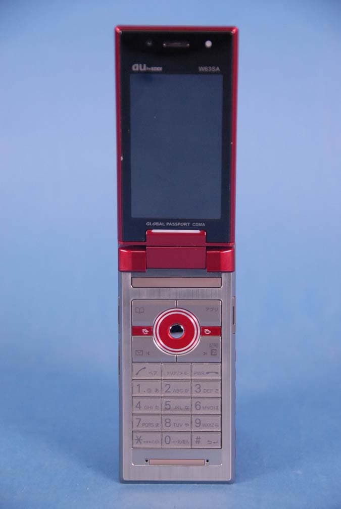
AEZW63SA
Mar 30, 2008Cellular CDMA Phone with Bluetooth
Equipment Class
TNE - Licensed Non-Broadcast Transmitter Held to Ear
AEZSCP-3800
Mar 09, 2008Cellular/ PCS CDMA Phone with Bluetooth
Equipment Class
JBP - Part 15 Class B Computing Device Peripheral
AEZSCP-25H
Sep 12, 2007Cellular/ PCS CDMA Phone with Bluetooth
Equipment Class
DSS - Part 15 Spread Spectrum Transmitter
AEZCPE-400-2C0
Jun 14, 2007W-CDMA subscriber terminal
Equipment Class
TNB - Licensed Non-Broadcast Station Transmitter
AEZNVM-4070
Jun 04, 2007PND (Personal Navigation Device)
Equipment Class
DXT - Part 15 Low Power Transceiver, Rx Verified