ALH29351110VHF-FM Transceiver
Kenwood USA Corporation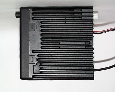
Click to zoom
Application Details
- Equipment Class
- TNB - Licensed Non-Broadcast Station Transmitter
- Date of Grant
- Mar 26, 2000
- Application Purpose
- Original Equipment
- Date of Application
- Feb 10, 2000
- Equipment Note
- VHF-FM Transceiver
- Frequency Range
- 29.70000000 - 37.00000000
- Company
- Kenwood USA Corporation
- Country
- United States
Documents & Files
Document Text
Text extracted from the exhibit documents filed with the FCC. Open a document above to read the original.
Users Manual
TK-6110 INSTRUCTION MANUAL VHF FM TRANSCEIVER © B62-1216-00 (K,K2) 09 08 07 06 05 04 03 02 01 00 KENWOOD CORPORATION THANK YOU! We are grateful you chose KENWOOD for your land mobile applications. We believe this easy-to-use transceiver will provide dependable communications to keep personnel operating at peak efficiency. KENWOOD transceivers incorporate the latest in advanced technology. As a result, we feel strongly that you will be pleased with the quality and features of this product. i One or more of the following statements may be applicable: FCC WARNING This equipment generates or uses radio frequency energy. Changes or modifications to this equipment may cause harmful interference unless the modifications are expressly approved in the instruction manual. The user could lose the authority to operate this equipment if an unauthorized change or modification is made. INFORMATION TO THE DIGITAL DEVICE USER REQUIRED BY THE FCC This equipment has been tested and found to comply with the limits for a Class B digital device, pursuant to Part 15 of the FCC Rules. These limits are designed to provide reasonable protection against harmful interference in a residential installation. This equipment generates, uses and can generate radio frequency energy and, if not installed and used in accordance with the instructions, may cause harmful interference to radio communications. However, there is no guarantee that the interference will not occur in a particular installation. If this equipment does cause harmful interference to radio or television reception, which can be determined by turning the equipment off and on, the user is encouraged to try to correct the interference by one or more of the following measures: •Reorient or relocate the receiving antenna. •Increase the separation between the equipment and receiver. •Connect the equipment to an outlet on a circuit different from that to which the receiver is connected. •Consult the dealer for technical assistance. uGOVERNMENT LAW PROHIBITS THE OPERATION OF UNLICENSED RADIO TRANSMITTERS WITHIN THE TERRITORIES UNDER GOVERNMENT CONTROL. uILLEGAL OPERATION IS PUNISHABLE BY FINE OR IMPRISONMENT OR BOTH. uREFER SERVICE TO QUALIFIED TECHNICIANS ONLY. SAFETY: It is important that the operator is aware of, and understands, hazards common to the operation of any transceiver. WARNING! uEXPLOSIVE ATMOSPHERES (GASES, DUST, FUMES, etc.) Turn OFF your transceiver while taking on fuel or while parked in a gasoline service station. Do not carry spare fuel containers in the trunk of your vehicle if your transceiver is mounted in the trunk area. uINJURY FROM RADIO FREQUENCY TRANSMISSIONS Do not operate your transceiver when somebody is within two to three feet of the antenna, to avoid the possibility of radio frequency burns or related physical injury. uDYNAMITE BLASTING CAPS Turn OFF your transceiver when in an area where blasting is in progress, or where “TURN OFF TWO-WAY RADIO” signs have been posted. Operating the transceiver within 150 meters (500 feet) of dynamite blasting caps may cause them to explode. If you are carrying blasting caps in your vehicle, make sure they are enclosed in a metal box with a padded interior. Do not transmit while the caps are being placed into or are being removed from the container. Note: This instruction manual covers only the basic functions of the transceiver. Consult your dealer for more detailed information. NOTICES TO THE USER ii CONTENTS UNPACKING AND CHECKING EQUIPMENT ................................... 1 Supplied Accessories ................................................................. 1 PREPARATION .................................................................................. 2 Tools Required ............................................................................. 2 Power Cable Connection ............................................................ 2 Installing the Transceiver ........................................................... 3 GETTING ACQUAINTED ................................................................... 4 Front Panel ................................................................................... 4 Display .......................................................................................... 5 Rear Panel .................................................................................... 6 Microphone .................................................................................. 6 PROGRAMMABLE FUNCTIONS ...................................................... 7 BASIC OPERATIONS ...................................................................... 10 Switching Power ON/ OFF ........................................................ 10 Adjusting the Volume ................................................................ 10 Selecting a Channel ................................................................... 10 Making a Call .............................................................................. 10 DTMF CALLS .................................................................................... 11 Manual Dialing ............................................................................ 11 Redialing ...................................................................................... 11 Auto Dialing ................................................................................. 11 AUXILIARY FUNCTIONS ................................................................. 13 Time-out Timer (TOT) ................................................................ 13 Busy Channel Lockout (BCL) ................................................... 13 2-Tone/ DTMF Signaling ............................................................ 13 Roll Over/ Dead End .................................................................. 13 Dead Beat Disable (DBD) .......................................................... 14 Timed Power OFF .............................................................…
Text truncated - open the document above for the full version.
Block Diagram
TK-6110 BLOCK DIAGRAM RF X57-610 Block diagram Model name:TK-6110K(FCC ID:ALH29351110) Model name:TK-6110K2(FCC ID:ALH29351120)
External Photos
Bottom View Model name:TK-6110 FCC ID:ALH29351110
External Photos
Front View Model name:TK-6110 FCC ID:ALH29351110
External Photos
Left Side View Model name:TK-6110 FCC ID:ALH29351110
External Photos
Rear View Model name:TK-6110 FCC ID:ALH29351110
External Photos
Right Side View Model name:TK-6110 FCC ID*ALH29351110
ID Label/Location Info
Name plate Model name:TK-6110K :TK-6110K2 FCC ID:ALH29351110 :ALH29351120
Internal Photos
PC Board Bottom View Model name:TK-6110 FCC ID:ALH29351110
Internal Photos
PC Board Top View Model name:TK-6110 FCC ID:ALH29351110
Internal Photos
PC Board Top View Model name:TK-6110 FCC ID:ALH29351110
Internal Photos
PC Board Bottom View Model name:TK-6110 FCC ID:ALH29351110
Operational Description
FCC ID:ALH29351110(TK-6110 K) FCC ID:ALH29351120(TK-6110 K2) TK-6110 Circuit Description The KENWOOD model TK-6110 is a VHF/FM mobile transceiver designed to operate in the frequency range of 29.7 to 50 MHz. 29.7-37MHz TK-6110K1(FCC ID:ALH29351110),35-50MHz TK-6110K2(FCC ID:ALH29351120) The unit consists of a receiver, a transmitter, a phase-locked loop (PLL) frequency synthesizer, a digital control unit, power supply circuits and a signaling unit. 1. RECEIVER CIRCUIT The receiver is double conversion superheterodyne, designed to operate in the frequency range of 29.7MHz to 50MHz. 1.1 FRONT-END RF AMPLIFIER An incoming signal from the antenna is applied to a band-pass filter (L202) after going through a low-pass filter and an antenna switch (K1). The signal is then amplified by the RF amplifier (Q201) and again filtered by another band-pass filter (L203,L206 and L207). 1.2 FIRST MIXER The signal from the band-pass filter is heterodyned with the first local oscillator signal from the PLL frequency synthesizer circuit at the first mixer (IC201) to become a 128.55MHz first intermediate frequency (IF) signal. The first IF signal is fed through two monolithic crystal filters (XF201) to further remove spurious signals. 1.3 IF AMPLIFIER The first IF signal is amplified by Q202 and Q205, and then enters IC202 (FM processing IC).The signal is heterodyned again with a second local oscillator signal(129.005MHz) with in IC202 to become a 455kHz second IF signal. The second IF signal is fed through a 455kHz ceramic filter, CF201 and CF202 to further eliminate unwanted signals before it is amplified and FM detected in IC202. 1.4 AUDIO AMPLIFIER The recovered audio signal obtained from IC202 is amplified by IC709, IC713, low-pass filtered by IC713 high-pass filtered by IC713 and band-eliminate filtered by IC713. The audio signals then passed through a de-emphasized by IC713. The processed audio signal passes through an audio volume control and is amplified to a sufficient level to drive a loudspeaker by an audio power amplifier BTL(IC102). 1.5 SQUELCH CIRCUIT The output signal from IC202 enters FM IC again, then passed through a band-pass filter. The noise component output from IC202 is amplified by Q206 and rectified by D205 to produce a DCvoltage corresponding to the noise level. The DC voltage is sent to the analog port of the CPU(IC604). And IC202 outputs a DC voltage(RSSI)corresponding to the input of the IF amplifier. 2. TRANSMITTER 2.1 MICROPHONE CIRCUIT FCC ID:ALH29351110(TK-6110 K) FCC ID:ALH29351120(TK-6110 K2) The signal from the microphone is high-pass filtered by IC713, passed through microphone mute and microphone amplifier circuit (Q703 and IC714), limited and pre-emphasized by IC713,D711. 2.2 MODULATOR CIRCUIT The output of the Audio-processor (IC713) is passed to the D/A converter (IC710) for maximum deviation adjustment and the summing amplifier (IC711) before being applied to a varactor diode in the voltage controlled oscillator (VCO) located in the frequency synthesizer section. 2.3 DRIVER AND FINAL POWER AMPLIFIER CIRCUITS The transmit signal is generated by the TX mixer(Q503). The transmit signal obtained from the buffer amplifier Q1 and Q2, is amplified by Q3 to approximately 30dBm. This amplified signal is amplified by Q4 and Q5 to approximately 8W. and this signal is passed to the FINAL stage. The RF power amplifier consists of transistor (Q6 and Q7) and is capable of producing up to 70W of RF power. 2.4 TRANSMIT/RECEIVE SWITCHING CIRCUIT The final output signal is passed through a transmit/receive switching circuit (K1) before it is passed to the antenna terminal. 2.5 AUTOMATIC POWER CONTROL, CIRCUIT AND TRANSMITTER The APC circuit consists of a RF level detector, an exciter control section and a temperature sensing circuit. The RF level detector senses the forward and reflected power. The transmitter output power is kept constant by the exciter control circuit which monitors the forward power and regulates the supply voltage applied to the exciter section. If the antenna load becomes abnormal, the reflected power increases, causing the exciter control circuit to reduce the supply voltage to the exciter. In case of an abnormal temperature rise in the power amplifier section, the temperature sensing circuit detects this condition and send the information to the APC circuit. These actions reduce the transmitter output power to a safe operating level. 3. PLL FREQUENCY SYNTHESIZER 3.1 PLL The frequency step of the PLL circuit is 5 kHz. A 16.8MHz reference oscillator signal is divided at IC501 by a fixed counter to produce the 5 kHz reference frequency. The VCO output signal is buffer amplified by Q505 and Q504, then divided in IC501, by a dual-modules programmable counter in this case. The divided signal is compared in phase with the 5 kHz reference signal in the phase comparator also in IC501. The output signal from the phase comparator is low-pass filtered and passed to the VCO to control the oscillator frequency. 3,.2 VOLTAGE CONTROLLED OSCILLATOR (VCO) The operating frequency is generated by Hybrid Integrated Circuit(HIC) in transmit mode and HIC in receive mode. The oscillator frequency is controlled by applying the VCO control voltage, obtained from the phase comparator to the varactor diodes. 3.3 UNLOCK DETECTOR CIRCUIT If a pulse signal appears at the LD pin of IC501, an unlock condition occurs, the voltage applied to the UL pin of the microprocessor to go low. When the microprocessor detects this condition, the FCC ID:ALH29351110(TK-6110 K) FCC ID:ALH29351120(TK-6110 K2) transmitter is disabled by ignoring the push-to-talk switch input signal. 4. DIGITAL CONTROL CIRCUIT 4.1 KEY SWITCHES CIRCUIT The key switches in formation are entered into the microprocessor (IC604) after passing through a IC901. 4.2 RESET CIRCUIT When the power is initially turned on, the reset circuit (IC601). 4.3 LAMP CIRCUIT An LED is provided to illuminate the LCD and its operation is controlled by …
Text truncated - open the document above for the full version.
Parts List/Tune Up Info
FCC ID:ALH29351110(TK-6110K ) FCC ID:ALH29351120(TK-6110K2) TK-6110SEMICONDUCTOR LIST CIRCUITPARTSDESCRIPTIONFOR MODEL : TK-6110 SYMBOLNUMBER<X57-6100-10><X57-6100-11> D1HSM88AS DIODEREFLECTED WAVE RECTIFICATION D202DZ5.1(Y) ZENER DIODEVOLTAGE PROTECTION D3HSM88AS DIODEFORWARD WAVE RECTIFICATION D41SS355 DIODESURGE ABSORPTION D51SS355 DIODEPROTECTOR D101DSA3A1-FK DIODEREVERSE PROTECTION D102ZSA5A27 ZENER DIODEVOLTAGE PROTECTION D10302DZ15(X,Y) ZENER DIODEVOLTAGE PROTECTION D1041SS355 DIODEDC SWITCH D10502DZ15(X,Y) ZENER DIODEVOLTAGE PROTECTION D1061SS355 DIODEDC SWITCH D107DA204U DIODESURGE ABSORPTION D1081SS355 DIODEDC SWITCH D10902DZ18(X,Y) ZENER DIODEVOLTAGE PROTECTION D202KV1470 VARIABLE CAPACITANCE DIODEB.P.F. TUNING D203KV1470 VARIABLE CAPACITANCE DIODEB.P.F. TUNING D204KV1470 VARIABLE CAPACITANCE DIODEB.P.F. TUNING D205KV1470 VARIABLE CAPACITANCE DIODEB.P.F. TUNING D206MA742 DIODENOISE DETECTION D207MA2S111 DIODEDC SWITCH D20802DZ5.1(Y) ZENER DIODEVOLTAGE PROTECTION D4011SS301 DIODEDC SWITCH D501MA2S077 DIODETX/RX SWITCH D502MA2S077 DIODETX/RX SWITCH D503MA2S077 DIODETX/RX SWITCH D504MA2S077 DIODETX/RX SWITCH D701DA204U DIODESURGE ABSORPTION D702DA204U DIODESURGE ABSORPTION D703DA204U DIODESURGE ABSORPTION D704DA204U DIODESURGE ABSORPTION D705DA204U DIODESURGE ABSORPTION D706DA204U DIODESURGE ABSORPTION D707DA204U DIODESURGE ABSORPTION D708DA204U DIODESURGE ABSORPTION D709DA204U DIODESURGE ABSORPTION D710DA204U DIODESURGE ABSORPTION D711MA742 DIODEVOLTAGE CLAMP D901B30-2151-05 LEDTX/BUSY LED D902B30-2140-05 LEDLCD BACK LIGHT D903B30-2140-05 LEDLCD BACK LIGHT D904B30-2140-05 LEDLCD BACK LIGHT D905B30-2140-05 LEDLCD BACK LIGHT D906B30-2140-05 LEDLCD BACK LIGHT D907B30-2140-05 LEDLCD BACK LIGHT D908B30-2050-05 LEDKEY BACK LIGHT D909B30-2050-05 LEDKEY BACK LIGHT D910B30-2050-05 LEDKEY BACK LIGHT D911B30-2050-05 LEDKEY BACK LIGHT D912DAP202U DIODEERROR PROTECTION FCC ID:ALH29351110(TK-6110K ) FCC ID:ALH29351120(TK-6110K2) D913DAP202U DIODEERROR PROTECTION D914DAP202U DIODEERROR PROTECTION D915DAP202U DIODEERROR PROTECTION D9161SS373 DIODESPEED UP IC2TA75S01F ICAPC COMPARATOR IC101TC4013BF(N) ICD FLIP-FLOP IC102TDA1519A ICAUDIO POWER AMP. IC103TA7808S ICVOLTAGE REGULATOR IC104TK11250BM ICVOLTAGE REGULATOR IC105BU4066BCFV ICANALOG SWITCH IC201GN2011(Q) ICACTIVE D.B.M. IC202TA31136FN ICFM IF SYSTEM IC203TC7S66FU ICAUDIO MUTE SWITCH IC401MC1350D ICAGC AMP. IC501 LMX2332LTMX ICPLL IC601PST9132NR ICVOLTAGE DETECTOR IC602TK11250BM ICVOLTAGE REGULATOR IC603TC7WU04FU ICBUFFER AMP. IC604 784214GC0618EU MPUMICROPROCESSOR IC605AT2408N10SI2.5 ICEEPROM IC606TC7S02FU ICADDRESS DECODER IC607AT29C020-90TI ICFLASH ROM IC701BU4094BCFV ICSHIFT RESISTER IC702BU4094BCFV ICSHIFT RESISTER IC703BU4094BCFV ICSHIFT RESISTER IC704BU4094BCFV ICSHIFT RESISTER IC705TA75W01FU ICACTIVE FILTER IC706TC75W51FU ICACTIVE FILTER IC707TC75W51FU ICBUFFER AMP. IC708LC73872M ICDTMF DECODER IC709TC75W51FU ICBUFFER AMP./ACTIVE FILTER IC710M62364FP ICD/A CONVERTER IC711TC75W51FU ICBUFFER AMP./SUMMING IC712BU4066BCFV ICANALOG SWITCH IC713TC35453F ICAUDIO PROCESSOR IC714TA75W01FU ICBUFFER AMP./AF AMP. IC715M62354GP ICD/A CONVERTER IC901BU4094BCF ICSHIFT RESISTER IC902LC75824W ICLCD DRIVER Q12SC4649(N,P) TRANSISTORRF AMP. Q22SC3357 TRANSISTORRF AMP. Q32SK3074 FETRF AMP. Q42SK3075 FETRF DRIVE AMP. Q52SK3075 FETRF DRIVE AMP. Q62SC2630 TRANSISTORRF FINAL AMP. Q72SC2630 TRANSISTORRF FINAL AMP. Q82SK1824 FETDC SWITCH Q102SK1824 FETDC SWITCH Q101DTA114EE TRANSISTORDC SWITCH Q102DTA114YE TRANSISTORDC SWITCH Q103DTA114EE TRANSISTORDC SWITCH Q104DTC114TE TRANSISTORDC SWITCH Q105DTA144TE TRANSISTORDC SWITCH Q106DTC114EE TRANSISTORDC SWITCH Q1072SK1824 FETDC SWITCH FCC ID:ALH29351110(TK-6110K ) FCC ID:ALH29351120(TK-6110K2) Q108DTC114EE TRANSISTORDC SWITCH Q1092SK1824 FETDC SWITCH Q1102SJ506(S) FETDC SWITCH Q111DTA114YE TRANSISTORDC SWITCH Q112DTC114TE TRANSISTORDC SWITCH Q1132SK1824 FETDC SWITCH Q1142SK1824 FETDC SWITCH Q1152SK1824 FETDC SWITCH Q1172SB1132(Q,R) TRANSISTORDC SWITCH Q1182SA1362(Y) TRANSISTORDC SWITCH Q1192SA1362(Y) TRANSISTORDC SWITCH Q1212SK1824 FETDC SWITCH Q1222SK1824 FETDC SWITCH Q2012SK2596 FETRF AMP. Q202 2SK508NV(K52) FETIF AMP. Q2032SK508NV(K52) FETNB GATE Q2042SK508NV(K52) FETNB GATE Q2052SK1215(E) FETIF AMP. Q2062SC4617(S) TRANSISTORNOISE AMP. Q4013SK131(L) FETRF AMP. Q4022SA1832(GR) TRANSISTORAGC AMP. Q4032SC4738(GR) TRANSISTORAGC AMP. Q4042SC4738(GR) TRANSISTORRF AMP. Q4052SC4738(GR) TRANSISTORRF AMP. Q4062SC4738(GR) TRANSISTORRF AMP. Q4072SK1824 FETDC SWITCH Q4082SA1832(GR) TRANSISTORRF AMP. Q5012SC4617(S) TRANSISTORRIPPLE FILTER Q5033SK131(L) FETTX MIXER Q5042SC4617(S) TRANSISTORRF AMP. Q5052SC4649(N,P) TRANSISTORRF AMP. Q5062SC4649(N,P) TRANSISTORRF AMP. Q5072SC4617(S) TRANSISTORRF AMP. Q6012SK1824 FETDC SWITCH Q6022SK1824 FETDC SWITCH Q701DTD114EK TRANSISTORDC SWITCH Q702DTD114EK TRANSISTORDC SWITCH Q7032SJ243 FETAF SWITCH Q7042SK1824 FETDC SWITCH Q7052SJ243 FETAF SWITCH Q7062SK1824 FETDC SWITCH Q7072SK1824 FETDC SWITCH Q7082SK1824 FETMUTE SWITCH Q7092SK1824 FETDC SWITCH Q9012SC4617(S) TRANSISTORCURRENT DRIVER Q9022SC4617(S) TRANSISTORCURRENT DRIVER Q9032SK1824 FETDC SWITCH Q9042SK1824 FETDC SWITCH Q9052SK1824 FETDC SWITCH
Parts List/Tune Up Info
Parts list 1/3 Model name:TK-6110K :TK-6110K2 FCC ID:ALH29351110 :ALH29351120
Parts List/Tune Up Info
Parts list 2/3 Model name:TK-6110K :TK-6110K2 FCC ID:ALH29351110 :ALH29351120
Parts List/Tune Up Info
Parts list 3/3 Model name:TK-6110K :TK-6110K2 FCC ID:ALH29351110 :ALH29351120
Parts List/Tune Up Info
FCC ID:ALH29351110(TK-6110 K) FCC ID:ALH29351120(TK-6110 K2) TK-6110 Tuning procedure Before attempting to tune the transceiver, connect the unit to a suitable power supply. Whenever the transmitter tuned, unit must be connected to a suitable dummy load, unless the instruction specify otherwise. The speaker output connector must be terminated with a 4 Ohm dummy load at any time during the tuning and connected to an AC voltmeter and an audio distortion meter or a SINAD measurement at all the time during the tuning. Power sw on when connect to PC and FPU(KPG-46) cable with Radio. Select to "Program" from PC display then select "Test Mode" then ENTER. "Tuning Mode" when Select to F10. 1 Transmitter section 1.1 Frequency a. When Select "Frequency" then Enter. b. Select to Numbers for Frequency then Enter. 1.2 RF Power a. When Select "RF Power (Test)" then Enter. b. To Select Lower frequency, Center frequency, or Higher frequency, press Tab key. c. Select to Numbers for the RF Power then Enter. 1.3 Max Deviation a. When Select "Max, Deviation" then Enter. b. Select to Numbers for the Max, Deviation then Enter. 1.4 QT Deviation a. When Select "QT Deviation" then Enter. b. Select to Numbers for the QT Deviation then Enter. 1.5 DQT Deviation a. When Select "DQT Deviation" then Enter. b. Select to Numbers for the DQT Deviation then Enter. 1.6 DTMF Deviation a. When Select "DTMF Deviation" then Enter. b. Select to Numbers for the DTMF Deviation then Enter. 1.7 MSK Deviation a. When Select "MSK Deviation" then Enter. b. Select to Numbers for the MSK Deviation then Enter. 2 Receiver section 2.1 RX Sensitivity a. When Select "Sensitivity (Test)" then Enter. b. To Select Lower frequency, Center frequency, or Higher frequency, press Tab key. c. Select to Numbers for the Sensitivity then Enter. FCC ID:ALH29351110(TK-6110 K) FCC ID:ALH29351120(TK-6110 K2) 2.2 Squelch Tight. a. When Select "Squelch Tight (Test)" then Enter. b. To Select Lower frequency, Center frequency, or Higher frequency, press Tab key. c. Select to Numbers for the Squelch Tight then Enter. 2.3 Squelch Open a. When Select "Squelch Open (Test)" then Enter. b. To Select Lower frequency, Center frequency, or Higher frequency, press Tab key. c. Select to Numbers for the Squelch Open then Enter. 2.4 Select "Alt" when "Tuning mode" done.
Schematics
CIRCUIT SCHEMATIC(Display right) Model name:TK-6110K FCC ID:ALH29351110 Model name:TK-6110K2 FCC ID:ALH29351120
Schematics
CIRCUIT SCHEMATIC(Top Left) Model name:TK-6110K/TK-6110K2 FCC ID:ALH29351110/ALH29351120
Schematics
CIRCUIT SCHEMATIC(Top Right) Model name:TK-6110K/TK-6110K2 FCC ID:ALH29351110/ALH29351120
Schematics
CIRCUIT SCHEMATIC(Bottom Left) Model name:TK-6110K/TK-6110K2 FCC ID:ALH29351110/ALH29351120
Schematics
CIRCUIT SCHEMATIC(Bottom Right) Model name:TK-6110K/TK-6110K2 FCC ID:ALH29351110/ALH29351120
Schematics
CIRCUIT SCHEMATIC(Display left) Model name:TK-6110K FCC ID:ALH29351110 Model name:TK-6110K2 FCC ID:ALH29351120
Test Report
FCC ID: ALH29351110 MFA p0020003, d0020037 Date: February 10, 2000 Federal Communications Commission Via: Electronic Filing Attention: Authorization & Evaluation Division Applicant: Kenwood Communications Corporation Equipment: TK-6110-1 FCC ID: ALH29351110 FCC Rules: 90 Gentlemen: On behalf of the Applicant, enclosed please find Application Form 731, Engineering Test Report and all pertinent documentation, the whole for approval of the referenced equipment as shown. Filing fees are attached. We trust the same is in order. Should you need any further information, kindly contact the writer who is authorized to act as agent. Sincerely yours, William H. Graff, Director of Engineering enclosure(s) cc: Applicant WHG/cvr FCC ID: ALH29351110 MFA p0020003, d0020037 LIST OF EXHIBITS (FCC CERTIFICATION (TRANSMITTERS) - REVISED 9/28/98) APPLICANT: Kenwood Communications Corporation FCC ID: ALH29351110 BY APPLICANT: 1. LETTER OF AUTHORIZATION 2. IDENTIFICATION DRAWINGS, 2.1033(c)(11) LABEL LOCATION OF LABEL COMPLIANCE STATEMENT LOCATION OF COMPLIANCE STATEMENT 3. PHOTOGRAPHS, 2.1033(c)(12) 4. DOCUMENTATION: 2.1033(c) (3) USER MANUAL (9) TUNE UP INFO (10) SCHEMATIC DIAGRAM (10) CIRCUIT DESCRIPTION BLOCK DIAGRAM PARTS LIST ACTIVE DEVICES 5. PART 90.203(e) & (g) ATTESTATION BY M.F.A. INC. A. TESTIMONIAL & STATEMENT OF CERTIFICATION B. STATEMENT OF QUALIFICATIONS FCC ID: ALH29351110 MFA p0020003, d0020037 Sub-part 2.1033(c): EQUIPMENT IDENTIFICATION FCC ID: ALH29351110 NAMEPLATE DRAWING ATTACHED, EXHIBIT 1. LOCATION AS PER LABEL DRAWING(S) DATE OF REPORT February 10, 2000 SUPERVISED BY: William H. Graff, Director of Engineering FCC ID: ALH29351110 MFA p0020003, d0020037 THE APPLICANT HAS BEEN CAUTIONED AS TO THE FOLLOWING: 15.21 INFORMATION TO USER. The users manual or instruction manual for an intentional radiator shall caution the user that changes or modifications not expressly approved by the party responsible for compliance could void the user's authority to operate the equipment. 15.27(a) SPECIAL ACCESSORIES. Equipment marketed to a consumer must be capable of complying with the necessary regulations in the configuration in which the equipment is marketed. Where special accessories, such as shielded cables and/or special connectors are required to enable an unintentional or intentional radiator to comply with the emission limits in this part, the equipment must be marketed with, i.e. shipped and sold with, those special accessories. However, in lieu of shipping or packaging the special accessories with the unintentional or intentional radiator, the responsible party may employ other methods of ensuring that the special accessories are provided to the consumer, without additional charge. Information detailing any alternative method used to supply the special accessories for a grant of equipment authorization or retained in the verification records, as appropriate. The party responsible for the equipment, as detailed in § 2.909 of this chapter, shall ensure that these special accessories are provided with the equipment. The instruction manual for such devices shall include appropriate instructions on the first page of text concerned with the installation of the device that these special accessories must be used with the device. It is the responsibility of the user to use the needed special accessories supplied with the equipment. FCC ID: ALH29351110 MFA p0020003, d0020037 TABLE OF CONTENTS RULE DESCRIPTION PAGE . Test Report 1 2.1033(c) General Information Required 2 2.1033(c)(14) Rule Summary 5 . Standard Test Conditions and Engineering Practices 6 2.1046(a) Carrier Output Power (Conducted) 7 2.1051 Unwanted Emissions (Transmitter Conducted) 9 2.1053(a) Field Strength of Spurious Radiation 12 2.1049(c)(1) Emission Masks (Occupied Bandwidth) 15 2.1047(a) Audio Low Pass Filter (Voice Input) 18 2.1047(a) Audio Frequency Response 21 2.1047(b) Modulation Limiting 23 2.1055(a)(1) Frequency Stability (Temperature Variation) 25 2.1055(b)(1) Frequency Stability (Voltage Variation) 28 2.202(g) Necessary Bandwidth and Emission Bandwidth 29 FCC ID: ALH29351110 MFA p0020003, d0020037 PAGE NO. 1 of 29. Required information per ISO/IEC Guide 25-1990, paragraph 13.2: a) TEST REPORT b) Laboratory: (FCC: 31040/SIT) (Canada: IC 2044) M. Flom Associates, Inc. 3356 N. San Marcos Place, Suite 107 Chandler, AZ 85224 c) Report Number: d0020037 d) Client: Kenwood Communications Corporation P.O. Box 22745 Long Beach, CA 90801-5745 e) Identification: TK-6110-1 FCC ID: ALH29351110 Description: VHF FM Mobile Transceiver f) EUT Condition: Not required unless specified in individual tests. g) Report Date: February 10, 2000 EUT Received: February 2, 2000 h, j, k): As indicated in individual tests. i) Sampling method: No sampling procedure used. l) Uncertainty: In accordance with MFA internal quality manual. m) Supervised by: William H. Graff, Director of Engineering n) Results: The results presented in this report relate only to the item tested. o) Reproduction: This report must not be reproduced, except in full, without written permission from this laboratory. FCC ID: ALH29351110 MFA p0020003, d0020037 PAGE NO. 2 of 29. LIST OF GENERAL INFORMATION REQUIRED FOR CERTIFICATION IN ACCORDANCE WITH FCC RULES AND REGULATIONS, VOLUME II, PART 2 AND TO 90 Sub-part 2.1033 (c)(1): NAME AND ADDRESS OF APPLICANT: Kenwood Communications Corporation 2201 E. Dominguez St P.O. Box 22745 Long Beach, CA 90801-5745 MANUFACTURER: Kenwood Electronics Technologies PTE Ltd. 1 Ang Mo Kio Street 63 Singapore 569110 (c)(2): FCC ID: ALH29351110 MODEL NO: TK-6110-1 (c)(3): INSTRUCTION MANUAL(S): PLEASE SEE ATTACHED EXHIBITS (c)(4): TYPE OF EMISSION: 16K0F3E (c)(5): FREQUENCY RANGE, MHz: 29.7 to 37 (c)(6): POWER RATING, Watts: 70 Switchable Variable x N/A (c)(7): MAXIMUM POWER RATING, Watts: 300 FCC ID: ALH29351110 MFA p0020003, d0020037 PAGE NO. 3 of 29. M. Flom Associates, Inc. is accredited by the American Association for Laboratory Association (A2LA) as …
Text truncated - open the document above for the full version.
Contact Information
Applicant
Angelina Seay(Regulatory Support Engineer)
Technical Contact
M. Flom Associates, Inc.William H Graff
[email protected]480 926 3100
3356 N. San Marcos Place · Chandler, Arizona · United States
Non-Technical Contact
M. Flom Associates, Inc.Morton Flom
[email protected]480 926 3100
Test Firm
M. Flom Associates, Inc.Morton Flom
Technical Specifications
| # | Rule Parts | Frequency Range | Power Output | Emission | Tolerance |
|---|---|---|---|---|---|
| 1 | 90 | 29.7 MHz - 37 MHz | 70 W | 16K0F3E | 5.0000000000 ppm |
Other Applications from Kenwood USA Corporation
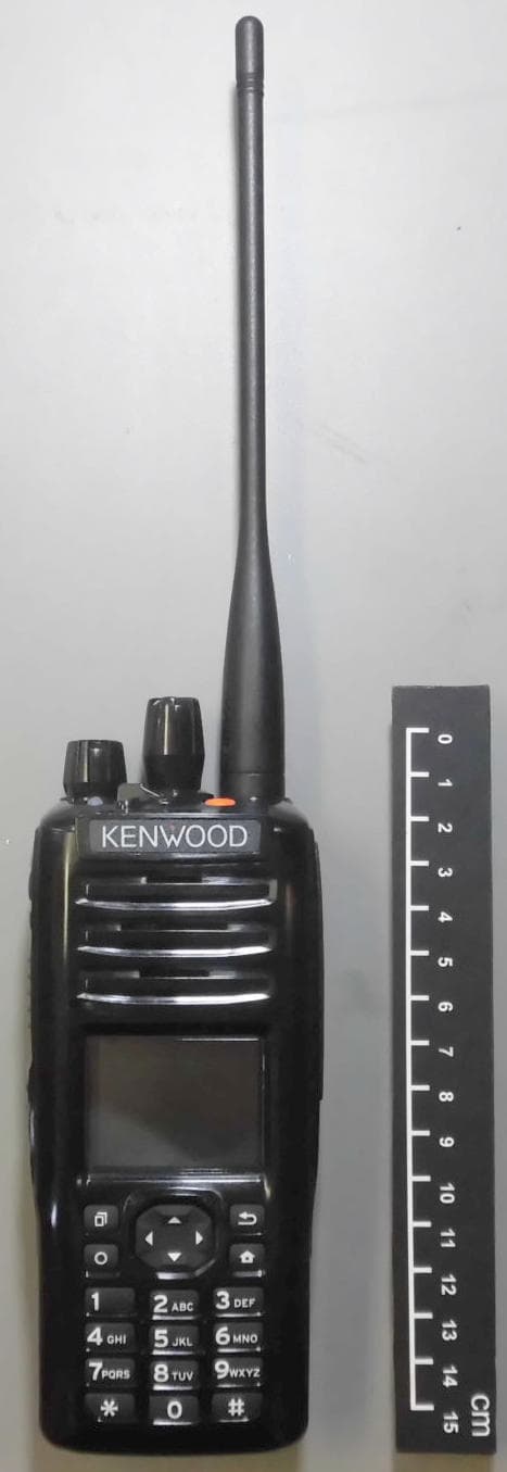
ALH442000
Jul 06, 2014Push to talk radio.
Equipment Class
DXX - Part 15 Low Power Communication Device Transmitter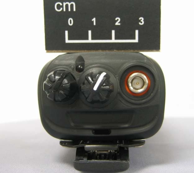
ALH443801
Dec 09, 2013UHF Digital Transceiver
Equipment Class
TNF - Licensed Non-Broadcast Transmitter Held to Face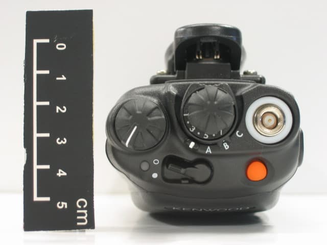
ALH468800
Oct 22, 2013PORTABLE LMR RADIO
Equipment Class
TNF - Licensed Non-Broadcast Transmitter Held to Face
ALH443700
Aug 18, 2013VHF Digital Transceiver Models NX-240-P, NX-240-K, NX-240-M, NX-240-M2, NX-240V-K
Equipment Class
TNF - Licensed Non-Broadcast Transmitter Held to Face
ALH443800
Aug 07, 2013Model NX-340 Digital Transceiver
Equipment Class
TNF - Licensed Non-Broadcast Transmitter Held to Face