ALH29521110VHF FM Transceiver
Kenwood USA Corporation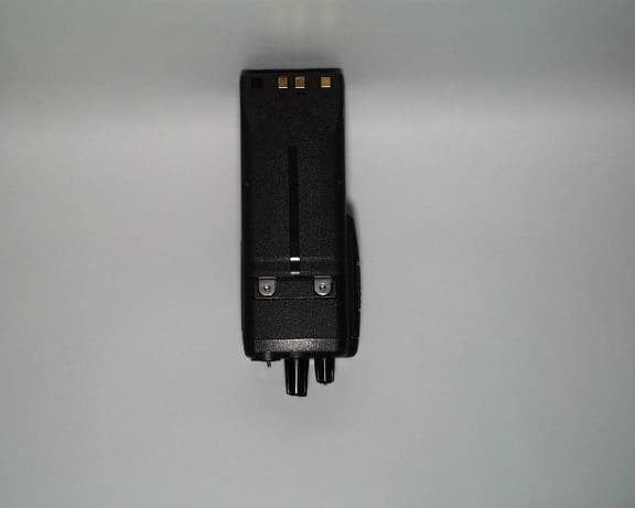
Click to zoom
Application Details
- Equipment Class
- TNF - Licensed Non-Broadcast Transmitter Held to Face
- Date of Grant
- Feb 16, 2000
- Application Purpose
- Original Equipment
- Date of Application
- Dec 08, 1999
- Equipment Note
- VHF FM Transceiver
- Frequency Range
- 29.70000000 - 37.00000000
- Company
- Kenwood USA Corporation
- Country
- United States
Documents & Files
Document Text
Text extracted from the exhibit documents filed with the FCC. Open a document above to read the original.
Users Manual
INSTRUCTION MANUAL © B62-1172-00 (K) 09 08 07 06 05 04 03 02 01 00 VHF FM TRANSCEIVER KENWOOD CORPORATION TK-190 uGOVERNMENT LAW PROHIBITS THE OPERATION OF UNLICENSED RADIO TRANSMITTERS WITHIN THE TERRITORIES UNDER GOVERNMENT CONTROL. uILLEGAL OPERATION IS PUNISHABLE BY FINE OR IMPRISONMENT OR BOTH. uREFER SERVICE TO QUALIFIED TECHNICIANS ONLY. uDO NOT OPERATE YOUR TRANSCEIVER IN EXPLOSIVE ATMOSPHERES (GASES, DUST, FUMES, ETC.). uTURN OFF YOUR TRANSCEIVER WHILE TAKING ON FUEL, OR WHILE PARKED IN GASOLINE SERVICE STATIONS. THANK YOU We are grateful you chose KENWOOD for your land mobile radio applications. We believe this easy-to-use transceiver will provide dependable communications to keep personnel operating at peak efficiency. KENWOOD transceivers incorporate the latest in advanced technology. As a result, we feel strongly that you will be pleased with the quality and features of this product. NOTICES TO THE USER SAFETY: It is important that the operator is aware of and understands hazards common to the operation of any transceiver. i One or more of the following statements may be applicable: ATTENTION (U.S.A. Only): The RBRC Recycle seal found on KENWOOD nickel-cadmium (Ni-Cd) battery packs indicates KENWOOD’s voluntary participation in an industry program to collect and recycle Ni-Cd batteries after their operating life has expired. The RBRC program is an alternative to disposing Ni-Cd batteries with your regular refuse or in municipal waste streams, which is illegal in some areas. For information on Ni-Cd battery recycling in your area, call (toll free) 1-800-8-BATTERY (1-800-822-8837). KENWOOD’s involvement in this program is part of our commitment to preserve our environment and conserve our natural resources. FCC WARNING This equipment generates or uses radio frequency energy. Changes or modifications to this equipment may cause harmful interference unless the modifications are expressly approved in the instruction manual. The user could lose the authority to operate this equipment if an unauthorized change or modification is made. INFORMATION TO THE DIGITAL DEVICE USER REQUIRED BY THE FCC This equipment has been tested and found to comply with the limits for a Class B digital device, pursuant to Part 15 of the FCC Rules. These limits are designed to provide reasonable protection against harmful interference in a residential installation. This equipment generates, uses and can generate radio frequency energy and, if not installed and used in accordance with the instructions, may cause harmful interference to radio communications. However, there is no guarantee that the interference will not occur in a particular installation. If this equipment does cause harmful interference to radio or television reception, which can be determined by turning the equipment off and on, the user is encouraged to try to correct the interference by one or more of the following measures: •Reorient or relocate the receiving antenna. •Increase the separation between the equipment and receiver. •Connect the equipment to an outlet on a circuit different from that to which the receiver is connected. •Consult the dealer for technical assistance. ii CONTENTS UNPACKING AND CHECKING EQUIPMENT.......................... 1 Supplied Accessories............................................. 1 PREPARATION.......................................................... 2 Installing/ Removing the Optional NiCd Battery Pack.......... 2 Installing the Optional Antenna.................................. 3 Installing the Belt Clip............................................ 3 Installing the Cover over the Universal Connector............ 4 Installing the Optional KMC-25 Speaker/ Microphone.......... 4 GETTING ACQUAINTED................................................ 5 Display ............................................................. 8 PROGRAMMABLE AUXILIARY FUNCTIONS......................... 9 Function Descriptions........................................... 10 OPERATING BASICS................................................. 14 Switching Power ON/OFF....................................... 14 Adjusting the Volume........................................... 14 Selecting a Channel............................................. 14 Making a Call.................................................... 15 Adjusting the Squelch........................................... 15 SCANNING............................................................ 16 Priority Scan..................................................... 17 Revert Channel.................................................. 18 SIGNALLING.......................................................... 19 2-Tone Signalling................................................ 19 DTMF Signalling................................................. 20 Dead Beat Disable (DBD)....................................... 21 PTT ID............................................................. 21 QUIET TALK (QT) AND DIGITAL QUIET TALK (DQT).............. 22 AUXILIARY FEATURES............................................... 23 Key Lock.......................................................... 23 Time-out Timer (TOT)........................................... 24 Busy Channel Lockout (BCL)................................... 24 Voice Scrambler................................................. 24 AUDIBLE USER FEEDBACK TONES................................. 26 1 UNPACKING AND CHECKING EQUIPMENT Note: The following unpacking instructions are for use by your KENWOOD dealer, an authorized KENWOOD service facility, or the factory. Carefully unpack the transceiver. We recommend that you identify the items listed in the following table before discarding the packing material. If any items are missing or have been damaged during shipment, file a claim with the carrier immediately. nSupplied Accessories metIrebmuNtraPytitnauQ koohtleBXX-2560-92J1 lasrevinU pacrotcennoc XX-3630-90B1 laeslennahCXX-4950-30B1 reppotslennahCXX-1240-23D1 te…
Text truncated - open the document above for the full version.
Block Diagram
TK-190 BLOCK DIAGRAMFCC ID:ALH29521110(TK-190K) FCC ID:ALH29521120(TK-190K2) +BATT SBC +B• ̈5V 2SK1824 SB B_Det DET=8.5V PST9132NR RN5VL54A 128.55MHz 158.25•`178.55MHz 158.705•`179.005MHz K:29.7•`37MHz k2: 35•`50MHz DET TCXO 16.8MHz 5TC 5RBC 455kHz PWR RSSI SQL 5RC 5TBC SW 5V Reg 5V SW 5V 5TB 5RB SW 5V 5C 3.58MHz STD 5RBC LSD 2Tone ASW EXT ESW ISW MUT DTMF AF A/D M62364FP NCSW EXT.MIC MIC MM TXOUT HSD DTMF_TX Option Audio Option Audio AF IC406 Microprocessor upc784214GC***8EU Adress Data DATA CLK INT 5R 5T INV DISPLAY X53-393 B/6 CONTROL X53-393 A/6 Rect 1SS184 Rect 1SS184 SP TK-190 129.005MHz SW 5V MIC SW 2SJ243/ DTC114EE INT.ANT LPF ANT SW D2 XB15A709 Power Amp Q1,2 2SK3075 (X45-361) Drive Amp Q2 2SK3074 Drive Amp Q1 2SC3356 Q32 2SC4649 RF Amp BPFRF Amp Q102 3SK131 BPF IC200 GN2011(Q) MCF Mixer IF Amp Q302 2SK1215 Mixer LPF APC Lo SW D102 DAN235E Q105 2SC4617(R) Buff Amp Q106 2SC4649 Buff Amp CD300CF300,301 FM System IC IC300 TA31136FN Q103 2SC4649 Buff Amp Q104 2SC4617(R) Buff Amp VCO1/2 L800 L78-0481-05 Dual PLL IC101 LMX2332LTMX SW IC301 TC7S66FU AF Amp Mute SW Q601 2SK1824 Fuse LPF DTMF Decoder IC600 LC73872M SUM Amp IC604(1/2) TC75W51FU Audio Processor IC607 TC35453F LPF LPF LPF LSD SUM Amp D/A convertor IC601 TC75W51FU TC75W01FU IC604(2/2) TC75W51FU Flash-ROM EERROM AT2408N10SI2.5 AT29C020-90TI Latch IC415 TC7S02FU Shift Register IC400,403,404,405 BU4094BCFV RF X57-608 L9,10,11 L201L202,206XF300 IC2 NJM2904V L103 L104 Q102 3SK131(L) Buff(INV) IC416 TC7WU04FU SWSW SW IC1 TDA7053AT SW NJM2904V MIC Amp AF Amp INT MIC (Main) INT MIC (N/C) IC3 D400 1SR154-40C Protect Power SW SB SW Q415 2SJ517 Q416 2SK1824 Regulate IC402 TK11250BM Regulate IC401 TK11250BM LCD LCD Driver IC101 LC73824W PF1 PF2 Togle SW TX,BUSY LED LAMP 5CC,5RC ,5TC SB SB SB SB SB 16.8MHz INV HPF IC417 TC7S04FU RESET IC407,IC409
Cover Letter(s)
ERATTA December 17, 1999 The Form 731 has an error. Please list power as: 1 to 6 watts Variable. Thanks, Bill Graff M. Flom Associates, Inc.
Operational Description
ALH29521110(TK-190K) ALH29521120(TK-190K2) TK-190 Circuit Description The KENWOOD model TK-190 is a VHF/FM hand-held transceiver designed to operate in the frequency range of 29.7 to 50 MHz. The unit consists of a receiver, a transmitter, a phase-locked loop (PLL) frequency synthesizer, a digital control unit, power supply circuits and a signaling unit. 1. RECEIVER CIRCUIT The receiver is double conversion superheterodyne, designed to operate in the frequency range of 29.7MHz to 50MHz. 1.1 FRONT-END RF AMPLIFIER An incoming signal from the antenna is applied to on RF amplifier (Q200) after passing through a transmit/receive switch circuit (D2 and D3 are off). After the signal is amplified, the signal is filtered by a Band-shift type band-pass filter to eliminate unwanted signals before it is routed to the first mixer. 1.2 FIRST MIXER The signal from the RF amplifier is heterodyned with the first local oscillator signal from the PLL frequency synthesizer circuit at the first mixer (IC200) to become a 128.55MHz first intermediate frequency (IF) signal. The first IF signal is fed through two monolithic crystal filters (XF300) to further remove spurious signals. 1.3 IF AMPLIFIER The first IF signal is amplified by Q302, and then enters IC300 (FM processing IC).The signal is heterodyned again with a second local oscillator signal(129.005MHz) with in IC300 to become a 455kHz second IF signal. The second IF signal is fed through a 455kHz ceramic filter, CF300 and CF301 to further eliminate unwanted signals before it is amplified and FM detected in IC300. 1.4 AUDIO AMPLIFIER The recovered audio signal obtained from IC300 is amplified by IC601,IC607, low-pass filtered by IC607 high-pass filtered by IC607 and band-eliminate filtered by IC607. The audio signals then passed through an audio frequency switch (Q8) and de-emphasized by IC607. The processed audio signal passes through an audio volume control and is amplified to a sufficient level to drive a loudspeaker by an audio power amplifier BTL(IC1). 1.5 SQUELCH CIRCUIT The output signal from IC300 enters FM IC again, then passed through a band-pass filter. The noise component output from IC300 is amplified by Q304 and rectified by D301 to produce a DC voltage corresponding to the noise level. The DC voltage is sent to the analog port of the CPU(IC406). And IC300 outputs a DC voltage(RSSI)corresponding to the input of the IF amplifier. 2. TRANSMITTER 2.1 MICROPHONE CIRCUIT The signal from the microphone is high-pass filtered by IC607, passed through microphone mute circuit (Q403), limited and pre-emphasized by IC607,D601. ALH29521110(TK-190K) ALH29521120(TK-190K2) 2.2 MODULATOR CIRCUIT The output of the Audio-processor (IC607) is passed to the D/A converter (IC603) for maximum deviation adjustment and the summing amplifier (IC605) before being applied to a varactor diode in the voltage controlled oscillator (VCO) located in the frequency synthesizer section. 2.3 DRIVER AND FINAL POWER AMPLIFIER CIRCUITS The transmit signal is generated by the TX mixer(Q102). The transmit signal obtained from the buffer amplifier Q32, is amplified by Q1 to approximately 16dBm. This amplified signal is amplified by Q2 to approximately 0.5W. and this signal is passed to the FINAL stage. The RF power amplifier consists of MOS FET transistor and is capable of producing up to 6W of RF power. 2.4 TRANSMIT/RECEIVE SWITCHING CIRCUIT The final output signal is passed through a transmit/receive switching circuit before it is passed to the antenna terminal. The transmit/receive switching circuit is comprised of D2 and D3. D2 and D3 are turned on (conductive) in transmit mode and turned off (isolated) in receive mode. 2.5 AUTOMATIC POWER CONTROL, CIRCUIT AND TRANSMITTER The automatic power control (APC) circuit stabilizes the transmitter output power at a pre-determined level by sensing the collector current of the final amplifier FET transistor in the final stage. The voltage comparator (IC2) compares the voltage obtained by the above collector current with a reference voltage, set using the microprocessor and Q4. An APC voltage proportional to the difference between the sensed voltage and the reference voltage appears at the output of IC2. This output voltage controls Q8, which in turn controls the voltage at pin 2 of the final unit, which keeps the transmitter output power constant. The transmitter output power can be varied to lW output power by the microprocessor, which in turn changes the reference voltage and hence the output power. 3. PLL FREQUENCY SYNTHESIZER 3.1 PLL The frequency step of the PLL circuit is 5 kHz. A 16.8MHz reference oscillator signal is divided at IC101 by a fixed counter to produce the 5 kHz reference frequency. The VCO output signal is buffer amplified by Q105,106, then divided in IC101, by a dual-modules programmable counter in this case. The divided signal is compared in phase with the 5 kHz reference signal in the phase comparator also in IC101. The output signal from the phase comparator is low-pass filtered and passed to the VCO to control the oscillator frequency. 3,.2 VOLTAGE CONTROLLED OSCILLATOR (VCO) The operating frequency is generated by Hybrid Integrated Circuit(HIC) in transmit mode and HIC in receive mode. The oscillator frequency is controlled by applying the VCO control voltage, obtained from the phase comparator to the varactor diodes. 3.3 UNLOCK DETECTOR CIRCUIT If a pulse signal appears at the LD pin of IC101, an unlock condition occurs, the voltage applied to the UL pin of the microprocessor to go low. When the microprocessor detects this condition, the transmitter is disabled by ignoring the push-to-talk switch input signal. ALH29521110(TK-190K) ALH29521120(TK-190K2) 4. DIGITAL CONTROL CIRCUIT 4.1 KEY SWITCHES CIRCUIT The key switches channel switches (channel selector) in formation are entered directly into the display microprocessor (IC406). 4.2 RESET CIRCUIT When the power is initially turned on, the reset circuit (IC409). …
Text truncated - open the document above for the full version.
Parts List/Tune Up Info
FCC ID:ALH29521110(TK-190 K) FCC ID:ALH29521120(TK-190K2) MODEL NUMBERMODEL NAME : TK-190 X53-3930-10<CONTROL UNIT>K,K2 SUBPART NUMBERTYPEPART NAMERATING FEATUERPROCASGRSPLYUNIT0-10REMARKSUPPLIER NZ92-0750-02 UNIT WIRING DIAGRAM 0 1 X NJ72-0705-02 9PRINTED WIRING BOARD180*150*1.0 40 5 1/2 E04-0403-05 9PIN SOCKET3P/12 40 12 CN 501502 E40-5662-05 9PIN ASS'Y SOCKET2P/1.25/16 40 11 CN 4 E40-5920-05 9FLAT CABLE CONNECTOR12P/0.5/24 40 11 CN 101 E40-5947-05 9FLAT CABLE CONNECTOR33P/0.5/32 40 11 CN 1 E40-5948-05 8FLAT CABLE CONNECTOR6P/0.5/16 40 11 CN 3 L92-0138-05 9FERRITE CHIP1608/8 40 11 L 101 L92-0141-05 9FERRITE CHIP 40 14 L 1234 L92-0149-05 9FERRITE CHIP2125/8/140 11 L 6 IMN10 8DIODE6P/8 40 11 D 16 MA2S111 9DIODE1608/2/8 40 15 D 1213151920 1SS373 9DIODE1608/2/8 40 11 D 101 B30-2019-05 9LED RE/GR/8 40 11 D 104 B30-2210-05 9LED TLY/8 40 12 D 102103 DTZ3.9(B) 9ZENER DIODE2P/8 40 11 D 2 2SB798(DL,DK) 9TRANSISTOR 40 11 Q 6 2SC4617(S) 9TRANSISTOR1608/3P/8 40 11 Q 5 UMC4 8TRANSISTOR5P/8 40 11 Q 14 2SK1824 9FET 3P/8 40 13 Q 7815 BU4094BCFV 9IC SSOP/16P/0.65/12 40 11 IC 2 LC75824W 7IC SOP/64P/0.5/T 40 11 IC 101 NJM2904V 9IC SSOP/8P/0.65/12 40 11 IC 3 TC7SH08FU 9IC SSOP5P/0.65/8 40 13 IC 456 N TC7W04FU 8IC SSOP/8P/0.65/12 40 11 IC 10 TDA7053AT 9IC SOP/16P/1.27/16 40 11 IC 1 R90-0723-05 9MULTIPLE RESISTOR 40 11 CP 1 R92-1252-05 9METAL GLAZE RESISTOR0/1A/1608/8 40 17 R 67811576263 RK73GB1J100J 9RESISTOR10/0.063W/1608/8 40 11 R 108 RK73GB1J470J 9RESISTOR47/0.063W/1608/8 40 11 R 3 RK73GB1J680J 9RESISTOR68/0.063W/1608/8 40 11 R 32 RK73GB1J101J 9RESISTOR100/0.063W/1608/8 40 12 R 3160 RK73GB1J102J 9RESISTOR1.0K/0.063W/1608/8 40 112 R 9101222234546474849 59502 RK73GB1J182J 9RESISTOR1.8K/0.063W/1608/8 40 12 R 3436 RK73GB1J222J 9RESISTOR2.2K/0.063W/1608/8 40 11 R 15 RK73GB1J332J 9RESISTOR3.3K/0.063W/1608/8 40 11 R 105 RK73GB1J472J 9RESISTOR4.7K/0.063W/1608/8 40 11 R 107 RK73GB1J103J 9RESISTOR10K/0.063W/1608/8 40 110 R 24526272835102103104 RK73GB1J153J 9RESISTOR15K/0.063W/1608/8 40 11 R 56 RK73GB1J183J 9RESISTOR18K/0.063W/1608/8 40 11 R 1 RK73GB1J223J 9RESISTOR22K/0.063W/1608/8 40 13 R 293033 RK73GB1J473J 9RESISTOR47K/0.063W/1608/8 40 15 R 1317184344 RK73GB1J104J 9RESISTOR100K/0.063W/1608/8 40 12 R 14101 RK73GB1J274J 9RESISTOR270K/0.063/1608/8 40 11 R 106 CC73GCH1H101J 9CERAMIC CAPACITOR100P50/1608/8 40 13 C 37104105 CK73FB1C104KTD 9CERAMIC CAPACITOR0.1U25/2125/8 40 11 C 14 CK73FB1C474K 9CERAMIC CAPACITOR0.47U16/2125/8 40 16 C 81213193032 CK73GB1C104K 9CERAMIC CAPACITOR0.1U/16V/1608/8 40 13 C 272829 CK73GB1E223K 9CERAMIC CAPACITOR0.022U25/1608/8 40 11 C 31 CK73GB1H471K 9CERAMIC CAPACITOR470P50/1608/8 40 113 C 123451522333439 434546 CK73GB1H102K 9CERAMIC CAPACITOR1000P50/1608/8 40 12 C 3538 C92-0602-05 8TANTALUM CAPACITOR1U/10V/8/2125 40 11 C 106 C92-0734-05 8TANTALUM CAPACITOR100U10V/12 40 11 C 16 DESTINATION & QTY ( REF.NO)
Parts List/Tune Up Info
FCC ID:ALH29521110(TK-190K) FCC ID:ALH29521120(TK-190K2) TK-190 Tuning procedure Before attempting to tune the transceiver, connect the unit to a suitable power supply. Whenever the transmitter tuned, unit must be connected to a suitable dummy load, unless the instruction specify otherwise. The speaker output connector must be terminated with a 4 Ohm dummy load at any time during the tuning and connected to an AC voltmeter and an audio distortion meter or a SINAD measurement at all the time during the tuning. Power sw on when connect to PC and FPU(KPG-36) cable with Radio. Select to "Program" from PC display then select "Test Mode" then ENTER. "Tuning Mode" when Select to F10. 1 Transmitter section 1.1R.F High Power a. When Select to "R.F High Power (Test)" then Enter. b. Same as "a" when Select to Lower frequency, Center frequency, Higher frequency then Enter. c. Select to Numbers for the R.F High Power then Enter. 1.2R.F Low Power a. When Select to "R.F Low Power" then Enter. b. Select to Lower frequency, Center frequency, Higher frequency. c. Select to Numbers for R.F Low Power then Enter. 1.3Max, Deviation a. When Select to "Max, Deviation" then Enter. b. Select to Numbers for the Max, Deviation then Enter. 1.4QT Deviation a. When Select to "QT Deviation" then Enter. b. Select to Numbers for the QT Deviation then Enter. 1.5DQT Deviation a. When Select to "DQT Deviation" then Enter. b. Select to Numbers for the QT Deviation then Enter. 1.6DTMF Deviation a. When Select to "DTMF Deviation" then Enter. b. Select to Numbers for the DTMF Deviation then Enter. 1.7MSK Deviation a. When Select to "MSK Deviation" then Enter. b. Select to Numbers for the MSK Deviation then Enter. 2 Receiver section 2.1RX Sensitivity a. When Select to "Sensitivity"(Test)" then Enter. b. Same as "a" when Select to Lower frequency, Center frequency, Higher frequency Then Enter. 2.2Squelch Tight. a. When Select to "Squelch Tight" then Enter. b. Same as "a" when Select to Lower frequency, Center frequency, Higher frequency Then Enter. FCC ID:ALH29521110(TK-190K) FCC ID:ALH29521120(TK-190K2) 2.3Squelch Open a. When Select to "Squelch Tight" then Enter. b. Same as "a" when Select to Lower frequency, Center frequency, Higher frequency Then Enter. 2.4Select "Alt" when "Tuning mode" done.
Test Report
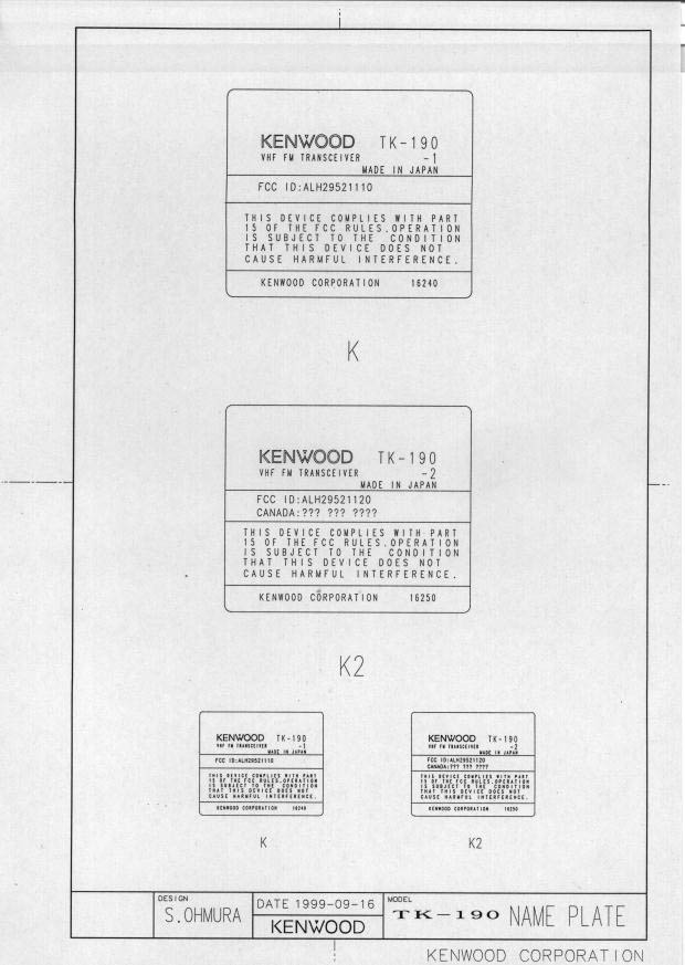
FCC ID: ALH29521110 MFA p99b0003, d99c0031 Date:December 9, 1999 Federal Communications Commission Via: Electronic Filing Attention:Authorization & Evaluation Division Applicant:Kenwood Communications Corporation Equipment:TK-190-1 FCC ID:ALH29521110 FCC Rules:22, 90 Gentlemen: On behalf of the Applicant, enclosed please find Application Form 731, Engineering Test Report and all pertinent documentation, the whole for approval of the referenced equipment as shown. Filing fees are attached. We trust the same is in order. Should you need any further information, kindly contact the writer who is authorized to act as agent. Sincerely yours, Morton Flom, P. Eng. enclosure(s) cc: Applicant MF/cvr FCC ID: ALH29521110 MFA p99b0003, d99c0031 LIST OF EXHIBITS (FCC CERTIFICATION (TRANSMITTERS) - REVISED 9/28/98) APPLICANT:Kenwood Communications Corporation FCC ID:ALH29521110 BY APPLICANT: 1. LETTER OF AUTHORIZATION 2. IDENTIFICATION DRAWINGS, 2.1033(c)(11) LABEL LOCATION OF LABEL COMPLIANCE STATEMENT LOCATION OF COMPLIANCE STATEMENT 3. PHOTOGRAPHS, 2.1033(c)(12) 4. DOCUMENTATION: 2.1033(c) (3)USER MANUAL (9)TUNE UP INFO (10)SCHEMATIC DIAGRAM (10) CIRCUIT DESCRIPTION 5. PART 90.203(e) & (g) ATTESTATION BY M.F.A. INC. A.TESTIMONIAL & STATEMENT OF CERTIFICATION B.STATEMENT OF QUALIFICATIONS FCC ID: ALH29521110 MFA p99b0003, d99c0031 Sub-part 2.1033(c): EQUIPMENT IDENTIFICATION FCC ID: ALH29521110 NAMEPLATE DRAWING ATTACHED, EXHIBIT 1. LOCATION AS PER LABEL DRAWING(S) DATE OF REPORT December 9, 1999 SUPERVISED BY:Morton Flom, P. Eng. FCC ID: ALH29521110 MFA p99b0003, d99c0031 THE APPLICANT HAS BEEN CAUTIONED AS TO THE FOLLOWING: 15.21INFORMATION TO USER. The users manual or instruction manual for an intentional radiator shall caution the user that changes or modifications not expressly approved by the party responsible for compliance could void the user's authority to operate the equipment. 15.27(a)SPECIAL ACCESSORIES. Equipment marketed to a consumer must be capable of complying with the necessary regulations in the configuration in which the equipment is marketed. Where special accessories, such as shielded cables and/or special connectors are required to enable an unintentional or intentional radiator to comply with the emission limits in this part, the equipment must be marketed with, i.e. shipped and sold with, those special accessories. However, in lieu of shipping or packaging the special accessories with the unintentional or intentional radiator, the responsible party may employ other methods of ensuring that the special accessories are provided to the consumer, without additional charge. Information detailing any alternative method used to supply the special accessories for a grant of equipment authorization or retained in the verification records, as appropriate. The party responsible for the equipment, as detailed in § 2.909 of this chapter, shall ensure that these special accessories are provided with the equipment. The instruction manual for such devices shall include appropriate instructions on the first page of text concerned with the installation of the device that these special accessories must be used with the device. It is the responsibility of the user to use the needed special accessories supplied with the equipment. FCC ID: ALH29521110 MFA p99b0003, d99c0031 TABLE OF CONTENTS RULEDESCRIPTIONPAGE .Test Report1 2.1033(c)General Information Required2 2.1033(c)(14) Rule Summary5 .Standard Test Conditions and Engineering Practices6 2.1046(a) Carrier Output Power (Conducted)7 2.1051 Unwanted Emissions (Transmitter Conducted)9 2.1053(a) Field Strength of Spurious Radiation13 2.1049(c)(1) Emission Masks (Occupied Bandwidth)16 2.1047(a) Audio Low Pass Filter (Voice Input)21 2.1047(a) Audio Frequency Response24 2.1047(b) Modulation Limiting26 2.1055(a)(1) Frequency Stability (Temperature Variation)28 2.1055(b)(1)Frequency Stability (Voltage Variation)31 2.202(g) Necessary Bandwidth and Emission Bandwidth32 FCC ID: ALH29521110 MFA p99b0003, d99c0031 PAGE NO.1 of 32. Required information per ISO/IEC Guide 25-1990, paragraph 13.2: a)TEST REPORT b) Laboratory: (FCC: 31040/SIT) (Canada: IC 2044) M. Flom Associates, Inc. 3356 N. San Marcos Place, Suite 107 Chandler, AZ 85224 c) Report Number:d99c0031 d) Client:Kenwood Communications Corporation P.O. Box 22745 Long Beach, CA 90801-5745 e) Identification:TK-190-1 FCC ID: ALH29521110 Description:VHF FM Transceiver f) EUT Condition:Not required unless specified in individual tests. g) Report Date:December 9, 1999 EUT Received:November 1, 1999 h, j, k):As indicated in individual tests. i) Sampling method:No sampling procedure used. l) Uncertainty:In accordance with MFA internal quality manual. m) Supervised by: Morton Flom, P. Eng. n) Results:The results presented in this report relate only to the item tested. o) Reproduction: This report must not be reproduced, except in full, without written permission from this laboratory. FCC ID: ALH29521110 MFA p99b0003, d99c0031 PAGE NO.2 of 32. LIST OF GENERAL INFORMATION REQUIRED FOR CERTIFICATION IN ACCORDANCE WITH FCC RULES AND REGULATIONS, VOLUME II, PART 2 AND TO 22, 90 Sub-part 2.1033 (c)(1):NAME AND ADDRESS OF APPLICANT: Kenwood Communications Corporation 2201 E. Dominguez St P.O. Box 22745 Long Beach, CA 90801-5745 MANUFACTURER: Kenwood Corporation 14-6, Dogenzaka 1-Chome Shibuya-ku, Tokyo 150, Japan (c)(2):FCC ID:ALH29521110 MODEL NO:TK-190-1 (c)(3):INSTRUCTION MANUAL(S): PLEASE SEE ATTACHED EXHIBITS (c)(4):TYPE OF EMISSION:16K0F3E (c)(5):FREQUENCY RANGE, MHz: 29.7 to 37 (c)(6):POWER RATING, Watts:1 to 6 SwitchablexVariableN/A (c)(7):MAXIMUM POWER RATING, Watts:300 FCC ID: ALH29521110 MFA p99b0003, d99c0031 PAGE NO.3 of 32. M. Flom Associates, Inc. is accredited by the American Association for Laboratory Association (A2LA) as shown in the scope below. "This laboratory is accredited by the American Association for Laboratory Accreditation (A2LA) and the results shown in this report have been determined i…
Text truncated - open the document above for the full version.
Contact Information
Applicant
Angelina Seay(Regulatory Support Engineer)
Technical Contact
M. Flom Associates, Inc.Morton Flom
[email protected]480-926-3100
3356 N. San Marcos Pl., Suite 107 · Chandler, Arizona · United States
Non-Technical Contact
M. Flom Associates, Inc.Morton Flom
[email protected]480-926-3100
Test Firm
M. Flom Associates, Inc.Morton Flom
Technical Specifications
| # | Rule Parts | Frequency Range | Power Output | Emission | Tolerance |
|---|---|---|---|---|---|
| 1 | 22,90 | 29.7 MHz - 37 MHz | 6 W | 16K0F3E | 2.5000000000 ppm |
Other Applications from Kenwood USA Corporation
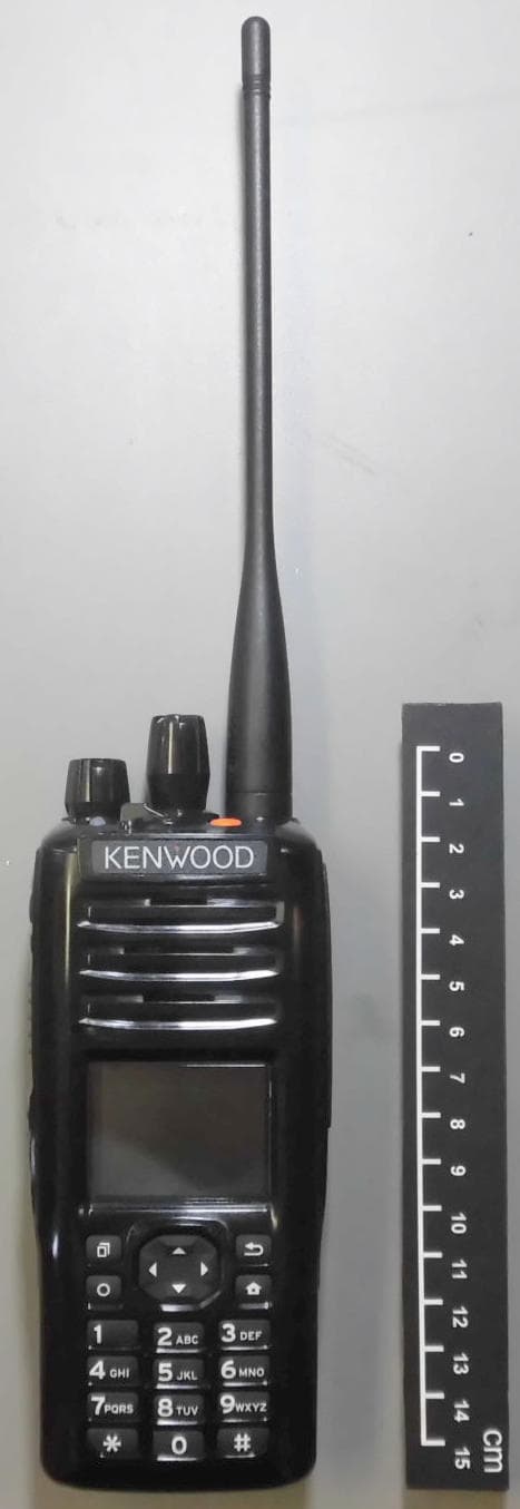
ALH442000
Jul 06, 2014Push to talk radio.
Equipment Class
DXX - Part 15 Low Power Communication Device Transmitter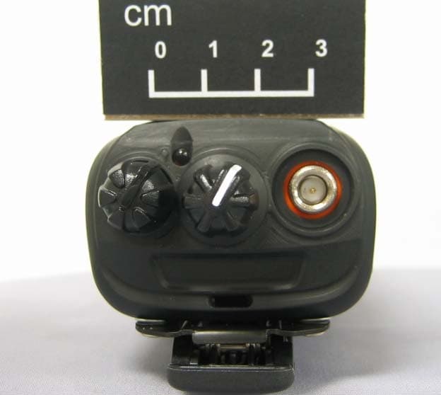
ALH443801
Dec 09, 2013UHF Digital Transceiver
Equipment Class
TNF - Licensed Non-Broadcast Transmitter Held to Face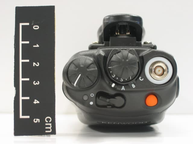
ALH468800
Oct 22, 2013PORTABLE LMR RADIO
Equipment Class
TNF - Licensed Non-Broadcast Transmitter Held to Face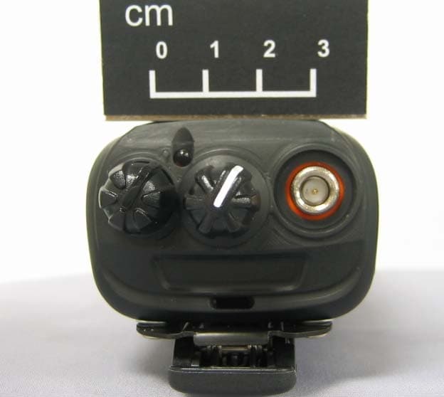
ALH443700
Aug 18, 2013VHF Digital Transceiver Models NX-240-P, NX-240-K, NX-240-M, NX-240-M2, NX-240V-K
Equipment Class
TNF - Licensed Non-Broadcast Transmitter Held to Face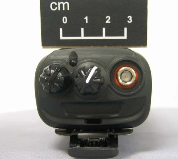
ALH443800
Aug 07, 2013Model NX-340 Digital Transceiver
Equipment Class
TNF - Licensed Non-Broadcast Transmitter Held to Face