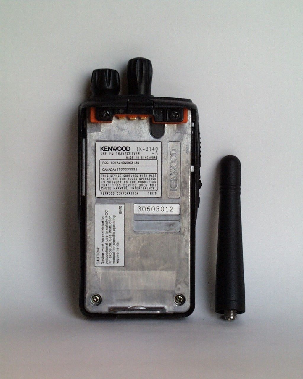
ALH32263130UHF Hand held to face
Kenwood USA Corporation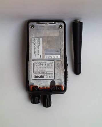
Click to zoom
Application Details
- Equipment Class
- TNF - Licensed Non-Broadcast Transmitter Held to Face
- Date of Grant
- Mar 13, 2002
- Application Purpose
- Original Equipment
- Date of Application
- Dec 13, 2001
- Equipment Note
- UHF Hand held to face
- Frequency Range
- 400.00000000 - 430.00000000
- Company
- Kenwood USA Corporation
- Country
- United States
Documents & Files
Document Text
Text extracted from the exhibit documents filed with the FCC. Open a document above to read the original.
Users Manual
© B62-XXXX-00 (K) 09 08 07 06 05 04 03 02 01 00 KENWOOD CORPORATION INSTRUCTION MANUAL VHF FM TRANSCEIVER TK-2140 TK-3140 UHF FM TRANSCEIVER i WARNING: EXPLOSIVE ATMOSPHERES (GASES, DUST, FUMES, etc.) Turn off your transceiver while taking on fuel, or while parked in gasoline service stations. uGOVERNMENT LAW PROHIBITS THE OPERATION OF UNLICENSED RADIO TRANSMITTERS WITHIN THE TERRITORIES UNDER GOVERNMENT CONTROL. uILLEGAL OPERATION IS PUNISHABLE BY FINE OR IMPRISONMENT OR BOTH. uREFER SERVICE TO QUALIFIED TECHNICIANS ONLY. SAFETY: It is important that the operator is aware of and understands hazards common to the operation of any transceiver. THANK YOU We are grateful you chose KENWOOD for your land mobile radio applications. We believe this easy-to-use transceiver will provide dependable communications to keep personnel operating at peak efficiency. KENWOOD transceivers incorporate the latest in advanced technology. As a result, we feel strongly that you will be pleased with the quality and features of this product. MODELS COVERED BY THIS MANUAL • TK-2140: VHF FM Transceiver • TK-3140: UHF FM Transceiver NOTICES TO THE USER ii One or more of the following statements may be applicable: ATTENTION (U.S.A. Only): The RBRC Recycle seal found on KENWOOD nickel-cadmium (Ni-Cd) battery packs indicates KENWOOD’s voluntary participation in an industry program to collect and recycle Ni-Cd batteries after their operating life has expired. The RBRC program is an alternative to disposing Ni-Cd batteries with your regular refuse or in municipal waste streams, which is illegal in some areas. For information on Ni-Cd battery recycling in your area, call (toll free) 1-800-8-BATTERY (1-800-822-8837). KENWOOD’s involvement in this program is part of our commitment to preserve our environment and conserve our natural resources. FCC WARNING This equipment generates or uses radio frequency energy. Changes or modifications to this equipment may cause harmful interference unless the modifications are expressly approved in the instruction manual. The user could lose the authority to operate this equipment if an unauthorized change or modification is made. INFORMATION TO THE DIGITAL DEVICE USER REQUIRED BY THE FCC This equipment has been tested and found to comply with the limits for a Class B digital device, pursuant to Part 15 of the FCC Rules. These limits are designed to provide reasonable protection against harmful interference in a residential installation. This equipment generates, uses and can generate radio frequency energy and, if not installed and used in accordance with the instructions, may cause harmful interference to radio communications. However, there is no guarantee that the interference will not occur in a particular installation. If this equipment does cause harmful interference to radio or television reception, which can be determined by turning the equipment off and on, the user is encouraged to try to correct the interference by one or more of the following measures: •Reorient or relocate the receiving antenna. •Increase the separation between the equipment and receiver. •Connect the equipment to an outlet on a circuit different from that to which the receiver is connected. •Consult the dealer for technical assistance. iii CONTENTS UNPACKING AND CHECKING EQUIPMENT................... 1 Supplied Accessories...................................... 1 PREPARATION.................................................. 2 Installing/ Removing the (Optional) Li-ion Battery Pack .. 2 Installing the (Optional) Antenna........................ 3 Installing the Belt Clip..................................... 3 Installing the Cover over the Universal Connector..... 4 Installing the (Optional KMC-25) Speaker/ Microphone ... 4 GETTING ACQUAINTED........................................ 5 Display...................................................... 7 PROGRAMMABLE AUXILIARY FUNCTIONS................. 8 OPERATION OVERVIEW....................................... 10 Trunking Format........................................... 10 Conventional Format..................................... 10 OPERATING BASICS........................................... 11 Switching Power ON/ OFF................................ 11 Adjusting the Volume..................................... 11 Selecting a System/ Group/ Channel................... 11 Time-out Timer (TOT).................................... 12 TRUNKED OPERATION (Trunking Format).................. 13 Placing a Dispatch Call.................................. 13 Receiving a Dispatch Call................................ 13 CONVENTIONAL OPERATION (Trunking Format)........... 14 Transmitting............................................... 14 Receiving.................................................. 14 iv SYSTEM SCAN (Trunking Format)........................... 15 Scanning Trunked Systems.............................. 15 Scanning Conventional Systems........................ 15 Scan Lockout.............................................. 16 Scan Revert................................................ 16 GROUP SCAN (Trunking Format)............................ 17 CONVENTIONAL OPERATION (Conventional Format)..... 18 Transmitting............................................... 18 Receiving.................................................. 18 SCAN (Conventional Format)................................ 19 Priority Scan............................................... 19 2-TONE SIGNALLING (Conventional Format).............. 20 FleetSync™: ALPHANUMERIC 2-WAY PAGING FUNCTION ...21 Key Functions............................................. 21 Selcall (Selective Calling)............................... 22 Status Message........................................... 23 Optional Short Messages Feature...................... 26 AUDIBLE USER FEEDBACK TONES.......................... 27 1 UNPACKING AND CHECKING EQUIPMENT Note: The following unpacking instructions are for use by your KENWOOD dealer, an authorized KENWO…
Text truncated - open the document above for the full version.
Block Diagram
1234567891011 HGFEDCBA USE FOR SYMBOL REVISION NO ISSUED DATE 12345 DESIGNED DRAWN CHECKED APPROVED PART NUMBERPART NAME 6789 - - - - - - - - - - - - - - - - - - KENWOODCORPORATION EX-3226 @D_APP @D_CHE @D_DRA JUNE/2001 @APPRO @CHECK @DRAWN @DESIG 01/10/31 09:05:30 ex3226blk.cir/001.sht 123456891071112131415161718192021222324252627282930 XOUTGNDAFCLRAFROTAFRTMAFTRDAFMSKECLKAFDATAFREG2AFREG1AFSTB5CNSMMUTE5TC5CGNDMICIPTTMEMETXHSDGNDTXAFRXAF15RCHSDINRXAFOGNDGND MUTE UPA672T 5TC MUTEMIC DC SW EMPHPRE Q501 Q501UPA672T AUDIO PROCESSOR IC500 DINDCK REGS1 REGS2 MSKE TRDRTMRDTCLREAF MUTE DTC144EE Q500MSKINEXPOTXOUT LC3872M TC35453F X500 3.579545MHz DTMF IN EXPGS TC75W51FU IC501 D501 RB706F-40 LIMITTER LPF MIC Q502 MICIN 2SK1830 PTT MICMUTE LPF LSDIN DTMF DECODE 5RC SD STDCLK TC75W51FU IC306 IC301 LC73872M DLK PD NOISE SQL PROTECT 5RC DET AMP NOISE AMP NOISE AMP NOISE DET MUTE Bias AMP IC300 TC75W51FU Q204 2SK1830 DET DM DISCHARGE TA31136FN D209MA2S111 RB706F-40 D201 2SC4617 Q208 TC75W51FU IC201 (TA31136FN) IC200 D200HVC131 DEO RF SW SW DTC144EE 455kHz GF(w) GF(N) 455kHz RF SW W/N CF200 CF201 D203DAN235E D202 DAN235E Q201 IC200 FM IF SYSTEM RSSI SHIFT MUTE DET Q202RN47A4 Q203 2SK1824 5RC X200 CD200 44.395MHz 455kHz IF AMP MCF 2SC4649 Q205 44.85MHz XF200 3SK318 1st Q206 MUTE BPF RF AMP HPF ANT SW LPF TUNE TUNE TV TV 5R 3SK318 Q207 UHFHVC369B 2 HVC369B 3UHF D204,205,206 D207-208 5T PROTECT DC SW 5T PCDC SW CURR DET Q105DTC114EEDTA144EEQ108 2SK1824 Q107 IC100 NJM2904V DC SW 5TC DTC114EE Q104 +B AMP AMP AMP DRIVE AMP DRIVE DRIVE FINAL T/R SW 5T 5T LPF 5R 2SK3476 Q106 Q103 2SK2596 Q101 2SC5192 5T Q100 2SC5108(Y) MA2S077X2 BUFF AMP 2SC5108(Y) Q8 AMP Q12SC5108(Y) BUFF D102-105HVC131 4 400-430MHz 5RCDTCLKDSTBEPFCLRHSDOLSDO5TCTXDAUXTXDAFTRDCPOEAFMSKEAFRTMEAFAFRTDSAVEAFSTBBEEPAFREG2W/NAFREG1 EN2RXDAUXRXDLSD1DTSTDTEMPRDTHSDIVOLRSSIASQLPFDTMDATULEN1SM IC309 30620M8A-2N3GPMICROPROCESSOR EXPANDEROUTPUTEXPANDEROUTPUT IC311 BU4094BCFV BU4094BCFV W/N5TC T/RAM1 DM LEDG LEDR MMUTE AFRG2 A0A4A15A17A12A18A7A3A2A10A13A6A5A8A16A9A11A14 RDWRD5D6D0CSOD2D3D7D4 AT29C020-90TI IC308 PROTECT MIC SP SSWSP+SP-MSWEMCMEPTTPFNCE5MTXD RXDE UNIVERSAL CONNECTOR TEMPCOMP 015AZ6.8D303 PROTECT 015AZ5.6 D304 2SC4617(S) Q304 5MS SW SW MSWSSW UPA672T Q305 2SJ347 Q301 SW UPA672T Q307 1SS373 D307 AM AFPA SW 2SK1824 Q308 SSW PROTECT TXRX UNIT X57-6410-10/11/12 PROTECT AVR SW TDA7053AT IC313 AVR SW 5R 2SC4617(S) Q309 2SC4617(S) Q306Q311 2SC4617(S)2SA1362(S) Q310 2SC4617(S)2SB1132(Q,R)015AZ2.4-X AM AF MIC NNCD6.8GD308 LG BUSY LR TXBACK LBL LIGHT B30-2157-05 D310 B30-2156-05 D309 4Key.AUX key LCD ASSY PTT LAMP MON DA221 X2 PROTECT D302/306 MICI AMP BUFF VCO D/A TV DTMF IN TC75W51FU IC303 PLL DTCPEP UL MD 2SC4617(S) Q7 5C T/R VCXO 16.8MHz X1 MB IC302 TC75W51FU TC75W51FU IC305 LPF TC75S01F IC304 HSDOUT AF MD FC PC TC75W51FU IC302 AMP BUFF M62364FP IC307 SB LATOR COMP AMP D19 LSDOUT HSDIN IC303TC75W51FU TC75W51FU HSDIN SW PROTECT AVR ENC X300 Q300 2SC4649 2SJ243 Q400,401 SW 2SK1830 5MS VOL TOP PANEL E PROM SCLSDA 2 D403 MA2S111 INT RST RESET DC SW AVR AVR DC SWDC SW BUFF PROTECT PROTECT INT IC404 D405 RB521S-30 D1 1SR154-400 IC403 IC401 IC400 IC402 2SJ347Q406 2SJ347 FUSE BATT7.5V + - + B SB 5M 5C 5R 5RC 5T 5TC 1/2 BIAS 5CNS SB CE CE BSHIFT SAVE D307 015AZ5.6 Q302Q303D305 IC201 Q311 SA7025DKIC1 IC300 Q405 Q404 IC300 AFRG1 AFCLR AFMSKE D100,101 IC312 SB BATTVDD 470-512MHz 450-490MHz 0-10 0-110-12 BLOCK DIAGRAM BSHIFT LCDBLT DISCHARGE 2SK508NV(K52) X2HVC376B X8 1SV278 2SJ347RN47A4 Q2,Q3 D5Q4Q6 FILTER LOOP RIPPLEFILTER SUM SUM 9.830MHz AT2416N10SI2.5 XC61CN5002NR XC6204B502MR XC6204B502MR XC61CN4202NR XC62GR5012PR KTA2015(Y) TC75W51FU DTMFPD TX D1-4,RX D7-10 UHF
Cover Letter(s)
August 27, 2001 Federal Communications Commission Authorization & Evaluation Division 7435 Oakland Mills Road Columbia, MD 21046 Gentlemen: This letter will authorize the appointment of MORTON FLOM, P. Eng. and/or M. Flom Associates, Inc. to act as our agent in all FCC matters. This appointment is effective until you are otherwise notified by us. This is to advise that we are in full compliance with the Anti-Drug Abuse Act. The application is not subject to a denial of federal benefits pursuant to section 5301 of the Anti-Drug Abuse Act of 1988, 21 USC 8.62, and no party to the application is subject to a denial of federal benefits pursuant to that section. Sincerely, Kenwood Communications Corporation Joel E. Berger Joel E. Berger Staff Engineer Research & Development Department Kenwood Communications Corporation Corporate Headquarters Kenwood Communications Corporation 3975 Johns Creek Court, Suite 300 Suwanee, GA 30024 678-474-4700 Distribution: 2201 E. Dominguez St. Long Beach, CA 90810 (310) 639-4200 Mailing Address: P.O. Box 22745 Long Beach, CA 90801-5745
Cover Letter(s)
August 27, 2001 Federal Communications Commission Authorization & Evaluation Division 7435 Oakland Mills Road Columbia, MD 21046 Gentlemen: Reference: This equipment meets the requirements of FCC Rules, Parts 90.203(e) and (g) as applicable. Programming of this product’s transmit frequencies can be performed ONLY by the manufacturer or by service or maintenance personnel. The operator cannot program transmit frequencies using the equipment’s external operation controls. Sincerely, Kenwood Communications Corporation Joel E. Berger Joel. E. Berger Staff Engineer Kenwood Communications Corporation Research & Development Department Corporate Headquarters Kenwood Communications Corporation 3975 Johns Creek Court, Suite 300 Suwanee, GA 30024 678-474-4700 Distribution: 2201 E. Dominguez St. Long Beach, CA 90810 (310) 639-4200 Mailing Address: P.O. Box 22745 Long Beach, CA 90801-5745
External Photos
FCC ID: ALH32263130 Model Name: TK-3140K3 Name Plate FCC ID: ALH32263130 Model Name: TK-3140K3 Front View FCC ID: ALH32263130 Model Name: TK-3140K3 Rear View FCC ID: ALH32263130 Model Name: TK-3140K3 To p Vi e w FCC ID: ALH32263130 Model Name: TK-3140K3 Bottom View FCC ID: ALH32263130 Model Name: TK-3140K3 Right View FCC ID: ALH32263130 Model Name: TK-3140K3 Left View
Internal Photos
FCC ID: ALH32263130 Model Name: TK-3140K3 PC Board: Front View FCC ID: ALH32263130 Model Name: TK-3140K3 PC Board: Rear View
Operational Description
FCC ID: ALH32263130 TK-3140 (K3)Specifications 1. General Frequency Ranges 400 MHz to 430 MHz (FCC ID: ALH32263130) Number of Channels 250 ch Channel Spacing 25 kHz (Wide)/12.5 kHz (Narrow) Types of Emission 16K0F3E (Wide) / 11K0F3E (Narrow) Power Supply Voltage 7.5 V 20% DC Nominal Antenna Impedance 50 Ω Operating Temperature -30 °C to +60 °C Dimension W. 56 mm x D.37(29.5) mm x H. 106 mm 2. Receiver Conversion Type Double Conversion Superheterodyne Intermediate Frequencies 1st 44.85 MHz (Lower) 2nd 455 kHz (Lower) Sensitivity (12dB SINAD) -117 dBm Minimum Spurious and Images 65 dB Minimum Intermodulation 66 dB Minimum (Wide) / 59dB Minimum (Narrow) Adjacent Channel Rejection 70 dB Minimum (Wide) / 62dB Minimum (Narrow) Hum and Noise 42 dB Minimum (Wide) / 37dB Minimum (Narrow) Audio Output Power 500 mW Maximaum (5% distortion / 16 Ω) Frequency Stability ±2.5 ppm Current Consumption 75 mA Std-by 330 mA Operating 3. Transmitter Output Power 4 W (High Power) 1 W (Low Power) Maximum Deviation ±5.0 kHz (Wide) / ±2.5 kHz (Narrow) FM Hum and Noise 42 dB Minimum (Wide) / 37 dB Minimum (Narrow) Audio Distortion 5 % Maximum Mic Sensitivity 15 mV (Nominal) Spurious and Harmonics Attenuation 65 dB minimum Frequency Stability ±2.5 ppm Current Consumption 2.0 A Maximum at 4 W output
Operational Description
FCC ID: ALH32263130 TK-3140(K3) Circuit Description The KENWOOD model TK-3140(K3) is a UHF/FM hand-held transceiver designed to operate in the frequency range of 400 to 430 MHz. (FCC ID: ALH32263130). The unit consists of a receiver, a transmitter, a phase-locked loop (PLL) frequency synthesizer, a digital control unit, power supply circuits and a signaling unit. 1. RECEIVER CIRCUIT The receiver is double conversion superheterodyne, designed to operate in the frequency range of 400MHz to 430MHz (FCC ID: ALH32263130). 1.1 FRONT-END RF AMPLIFIER An incoming signal from the antenna is applied to an RF amplifier (Q207) after passing through a transmit/receive switching circuit (D104 and D105 are off). After the signal is amplified, the signal is filtered by a Band-shift type band-pass filter to eliminate unwanted signals before it is routed to the first mixer. 1.2 FIRST MIXER The signal from the RF amplifier is heterodyned with the first local oscillator signal from the PLL frequency synthesizer circuit at the first mixer (Q206) to become a 44.85MHz first intermediate frequency (IF) signal. The first IF signal is fed through two monolithic crystal filters (MCFs: XF201) to further remove spurious signals. 1.3 IF AMPLIFIER The first IF signal is amplified by Q205, and then enters IC200 (FM IC).The signal is heterodyned again with a second local oscillator signal with in IC200 to become a 455kHz second IF signal. The second IF signal is fed through a 455kHz ceramic filter , CF200 (for Wide), CF201 (for Narrow) to further eliminate undesired signals before it is amplified and FM detected in IC200. 1.4 AUDIO AMPLIFIER The recovered audio signal obtained from IC200 is amplified by IC300, The audio signal is then passed through an audio frequency switch (Q204),low-pass filtered by IC500 high-pass filtered by IC500 and band-eliminate filtered by IC500. and de-emphasized by IC500. The processed audio signal passes through an audio volume control and is amplified to a sufficient level to drive a loudspeaker by an audio power amplifier (IC313) display board. 1.5 SQUELCH AND MUTE CIRCUIT The output signal from the squelch circuit, which consists of IC200,IC201 and Q208, is applied to the microprocessor. The microprocessor passes information to the shift register (IC311, IC312) and it controls the mute control lines (AF MUTE and AC) according to the input signal (noise pulse) and the microprocessor task condition. 2. TRANSMITTER 2.1 MICROPHONE CIRCUIT The signal from the microphone is high-pass filtered by IC500, passed through microphone mute circuit (Q501), limited and pre-emphasized by IC500. FCC ID: ALH32263130 2.2 MODULATOR CIRCUIT The output of the low-pass filter network (IC500) is passed to the D/A converter (IC307) for maximum deviation adjustment and the summing amplifier (IC305) before being applied to a varactor diode (D5) in the voltage controlled oscillator (VCO) located in the frequency synthesizer section. 2.3 DRIVER AND FINAL POWER AMPLIFIER CIRCUITS The transmit signal is directly generated by the VCO. The transmit signal obtained from the VCO buffer amplifier Q8, is amplified by Q100 and Q101, to approximately 17dBm. This amplified signal is passed to the power amplifier, Q103, Q106, consist of a 2-stage FET amplifier and is capable of producing up to 4W. 2.4 TRANSMIT/RECEIVE SWITCHING CIRCUIT The power module output signal is passed through a 3-stage low-pass filter network and a transmit/receive switching circuit before it is passed to the antenna terminal. The transmit/receive switching circuit is comprised of D102, D103. D104 and D105 are turned on (conductive) in transmit mode and turned off (isolated) in receive mode. 2.5 AUTOMATIC POWER CONTROL(APC)CIRCUIT AND TRANSMITTER OUTPUT LEVEL SWITCH The automatic power control (APC) circuit stabilizes the transmitter output power at a pre-determined level by sensing the collector current of the final RF amplifier FET. The voltage comparator (IC100) compares the voltage obtained by the above collector current with a reference voltage, set using the microprocessor and Q107. An APC voltage proportional to the difference between the sensed voltage and the reference voltage appears at the output of IC100. This output voltage controls the gate of the FET power amolifier, which keeps the transmitter output power constant. The transmitter output power can be varied to lW by the microprocessor, which in turn changes the reference voltage of IC300, and hence the output power. 3. PLL FREQUENCY SYNTHESIZER 3.1 PLL The frequency step of the PLL circuit is 5 or 6.25kHz. A 16.8MHz reference oscillator signal is divided at IC1 by a fixed counter to produce the 5 or 6.25kHz reference frequency. The VCO output signal is buffer amplified by Q1, then divided in IC1, by a dual-modules programmable counter in this case. The divided signal is compared in phase with the 5 or 6.25kHz reference signal in the phase comparator also in IC1. The output signal from the phase comparator is low-pass filtered and passed to the VCO to control the oscillator frequency. 3,.2 VOLTAGE CONTROLLED OSCILLATOR (VCO) The operating frequency is generated by voltage controlled oscilator (VCO) in transmit mode and VCO in receive mode. The oscillator frequency is controlled by applying the VCO control voltage, obtained from the phase comparator to the varactor diodes. The TX/RX pin is set high in receive mode causing IC312, and turn on. 3.3 UNLOCK DETECTOR CIRCUIT If a pulse signal appears at the LD pin of IC1, an unlock condition occurs, the DC voltage, causes the voltage applied to the UL pin of the microprocessor to go low. When the microprocessor detects this FCC ID: ALH32263130 condition, the transmitter is disabled by ignoring the push-to-talk switch input signal. 4. DIGITAL CONTROL CIRCUIT 4.1 KEY SWITCHES AND ROTARY ENCODER INPUT CIRCUIT The key switches and rotary encoder (channel selector) in formation are entered directly into the microprocessor (IC309). 4.2 RESET CIRCUIT …
Text truncated - open the document above for the full version.
Parts List/Tune Up Info
FCCID:ALH32263130 TK-3140(K3) Tuning procedure Before attempting to tune the transceiver, connect the unit to a suitable power supply. Whenever the transmitter tuned, unit must be connected to a suitable dummy load, unless the instruction specify otherwise. The speaker output connector must be terminated with a 16 Ohm dummy load at any time during the tuning and connected to an AC voltmeter and an audio distortion meter or a SINAD measurement at all the time during the tuning. Power sw on during "A" push to test mode [1-1] then push "S" to tuning mode. This *** mean using 3 numbers from CHANNEL NOB. 1 Transmitter section 1.1 Frequency adjustment Set test mode CH1,Push "S" to enter tuning mode, Select [FREQ***], then PTT on. 415.100MHz 50Hz. 1.2 TX High power adjustment Set test mode CH1,Push "S" to enter tuning mode, Select Hpow, Push "A" to 5 points. a) Select [L Hpow***] then PTT on 4.0W 0.1W. b) Push "C" to select [L2 Hpow***] then PTT on, push "B" after tuned. c) Push "C" to select [C Hpow ***] then PTT on, push "B" after tuned. d) Push "C" to select [H2Hpow***] then PTT on, push "B" after tuned. e) Push "C" to select [H Hpow***] then PTT on, push "S" to return test mode. The TX current is 2.2A or less. 1.3 TX Low power adjustment Set test mode CH1,Push "S" to enter tuning mode, Select L pow, Push "A" to 5 points. a) Select [L Lpow***] then PTT on 1.0W 0.1W. b) Push "C" to select [L2 Lpow***] then PTT on, push "B" after tuned. c) Push "C" to select [C Lpow***] then PTT on, push "B" after tuned. d) Push "C" to select [H2 Lpow***] then PTT on, push "B" after tuned. e) Push "C" to select [H Lpow***] then PTT on, push "S" to return test mode. The TX current is 1.0A or less. 1.4 DQT BAL adjustment Set test mode CH1,Push "S" to enter tuning mode, Select [BAL***], Push "A" to enter 3 Points, a) Select [LBAL***] adjustments mode then PTT on Push "B" after tuned . b) Push "C" to select [C BAL***] then PTT on push "B" after tuned. c) Push "C" to select [H BAL***] then PTT on push "B" after tuned. Push "A" to return to tuning mode. d) Push "Lamp" to narrow adjustment mode [n BAL***],then PTT on push "B" after tuned. Push "Lamp" to return tuning mode. Make the de-modulation waves into square waves. 1.5 Max deviation adjustment Set test mode CH1, push "S" to enter tuning mode, Push "A" to 3 points adjustment mode. a) Select [L MAX***] then PTT on push "B" after tuned. b) push "C" to select [C MAX***] then PTT on push "B" after tuned. FCCID:ALH32263130 c) push "C" to select [H MAX***] then PTT on push "B" after tuned Push "A" to return tuning mode. Deviation 3.80KHz(Wide), 1.75KHz(Narrow) Push " Lamp" to narrow adjustment mode [n MAX***] then PTT on push "Lamp" to return tuning mode. 1.6 QT Deviation adjustment a) Push "S" to enter tuning mode select [FQT***] push "A" to adjustment mode. Select [L FQT***] then PTT on push "B" after tuned. Deviation 0.75KHz.( 0.05KHz) (Wide) 0.35KHz ( 0.05KHz)(Narrow) b) same [C FQT***] c) same [H FQT***] d) same [n FQT***] 1.7 DQT Deviation adjustment a) Same as QT. Select [ FDQT***] b) same as [L FDQT***] c) same as [C FDQT***] d) same as [H FDQT***] e) same as [n FDQT***] Deviation 0.75KHz( 0.05KHz) (Wide) 0.35KHz ( 0.05KHz)(Narrow) 1.8 LTR Deviation adjustment a) Select [ FLTR***] b) Select [L FLTR***] c) Select [C FLTR***] d) Select [H FLTR***] e) Select [n FLTR***] Deviation 1.0KHz( 0.05KHz)(Wide) 0.75KHz( 0.05KHz)(Narrow) 1.9 DTMF Deviation adjustment a) Select [DTMF***] Deviation 3KHz( 0.05KHz)(Wide) b) Select [n DTMF***] Deviation 1.5KHz( 0.05KHz)(Narrow) 1.10 MSK Deviation adjustment a) Select [FMSK***] Deviation 3KHz( 0.05KHz)(Wide) b) Select [n MSK***] Deviation 1.5KHz( 0.05KHz)(Narrow) 2 Receiver section 2.1 Sensitivity a) Select [SENS***] , Push "A" to 5 points. b) Push "C" to select [L SENS***] to get best Sensitivity , then push "B" after tuned c) Push "C" to select [L2 SENS***] to get best Sensitivity , then push "B" after tuned d) Push "C" to select [C SENS ***] to get best Sensitivity , then push "B" after tuned e) Push "C" to select [H2 SENS***] to get best Sensitivity , then push "B" after tuned f) Push "C" to select [H SENS***] to get best Sensitivity , then push "B" after tuned g) push "A" to return test mode. 2.2 Open squelch adjustment FCCID:ALH32263130 a) Push “A” to 3 point ( SSG level : 12dB SINAD) b) Select [OSQL***] Adjust to point of opening squelch.(Wide) c) Select [OSQL***] Adjust to point of opening squelch d) Select [OSQL***] Adjust to point of opening squelch e) Select [n OSQL***] Adjust to point of opening squelch.(Narrow) 2.3 Tight squelch adjustment a) Push “A” to 3 point ( SSG level : 12dB SINAD + 5 dB) b) Select [TSQL***] Adjust to point of opening squelch.(Wide) c) Select [TSQL***] Adjust to point of opening squelch d) Select [TSQL***] Adjust to point of opening squelch f) Select [n TSQL***] Adjust to point of opening squelch.(Narrow)
Parts List/Tune Up Info
TK-3140K3 FCC ID:ALH32263130 TK-3140(K3) Semiconductor List REF.NO. PART NO. PART NAME Description D 202 203 DAN235E DIODE Switch D 302 306 DA221 DIODE surge absorption D 100 101 HSC277 DIODE RF switch D 102 103 104 105 HVC131 DIODE ANT switch D 6 MA2S111 DIODE Switch D 200 MA2S111 DIODE Switch D 209 MA2S111 DIODE Switch D 403 MA2S111 DIODE Switch D 405 RB521S-30 DIODE Protect D 200 RB706F-40 DIODE rectification D 300 RB706F-40 DIODE Bias D 501 RB706F-40 DIODE Protect D 402 1SR154-400 DIODE surge absorption D 301 1SS373 DIODE Protect D 309 B30-2156-05 LED LED D 310 B30-2157-05 LED LED D 2 4 9 10 HVC375B VARIABLE CAPACITANCE DIODE VCO D 1378 HVC376B VARIABLE CAPACITANCE DIODE VCO D 106 HZU5CLL ZENER DIODE Protect D 308 NNCD6.8G ZENER DIODE Protect D 305 015AZ2.4-X ZENER DIODE AVR D 303 304 307 015AZ6.8 ZENER DIODE Protect D 5 1SV278 VARIABLE CAPACITANCE DIODE VCO D 204 205 206 207 208 HVC369B VARIABLE CAPACITANCE DIODE BPF Tuning Q 311 2SA1362(Y) TRANSISTOR AVR Q 303 2SB1132(Q,R) TRANSISTOR AVR Q 7 2SC4617(S) TRANSISTOR AF AMP Q 208 2SC4617(S) TRANSISTOR AF AMP Q 302 2SC4617(S) TRANSISTOR AF AMP Q 304 2SC4617(S) TRANSISTOR AF AMP Q 306 2SC4617(S) TRANSISTOR AF AMP Q 309 2SC4617(S) TRANSISTOR AF AMP Q 310 2SC4617(S) TRANSISTOR AF AMP Q 205 2SC4649(N,P) TRANSISTOR IF AMP TK-3140K3 FCC ID:ALH32263130 REF.NO. PART NO. PART NAME Description Q 300 2SC4649(N,P) TRANSISTOR Switch Q 1 2SC5108(Y) TRANSISTOR RF AMP Q 5 2SC5108(Y) TRANSISTOR RF AMP Q 8 2SC5108(Y) TRANSISTOR RF AMP Q 100 2SC5108(Y) TRANSISTOR RF AMP Q 101 2SC5192 TRANSISTOR RF AMP Q 108 DTA144EE TRANSISTOR Switch Q 104 105 DTC114EE TRANSISTOR Switch Q 201 DTC144EE TRANSISTOR Switch Q 403 DTC144EE TRANSISTOR Switch Q 500 DTC144EE TRANSISTOR Switch Q 405 KTA2015(Y) TRANSISTOR Switch Q 6 RN47A4 TRANSISTOR Switch Q 503 RN47A4 TRANSISTOR Switch Q 305 UPA672T FET Switch Q 307 UPA672T FET Switch Q 501 UPA672T FET Switch Q 4 2SJ347 FET Switch Q 301 2SJ347 FET Switch Q 400 2SJ347 FET Switch Q 404 2SJ347 FET Switch Q 406 2SJ347 FET Switch Q 107 2SK1824 FET Switch Q 203 2SK1824 FET Switch Q 308 2SK1824 FET Switch Q 204 2SK1830 FET Switch Q 401 2SK1830 FET Switch Q 502 2SK1830 FET Switch Q 103 2SK2596 FET TX Drive AMP Q 106 2SK3476 FET TX Final AMP Q 2 2SK508NV(K52) FET VCO Q 3 2SK508NV(K52) FET VCO Q 206 3SK318 FET Front-end Q 207 3SK318 FET Front-end IC 310 AT2416N10SI2.5 ROM IC EEPROM TK-3140K3 FCC ID:ALH32263130 REF.NO. PART NO. PART NAME Description IC 311 312 BU4094BCFV MOS IC Shift Registor IC 301 LC73872M MOS IC DTMF Decoder IC 307 M62364FP MOS IC Potential Meter IC 1 SA7025DK MOS IC PLL IC 200 TA31136FN MOS IC IF IC 100 TA75W01FU MOS IC AF AMP IC 500 TC35453F MOS IC Base Band IC 304 TC75S51F MOS IC AF AMP,Filter IC 201 TC75W51FU MOS IC AF AMP,Filter IC 300 TC75W51FU MOS IC AF AMP,Filter IC 302 TC75W51FU MOS IC AF AMP,Filter IC 303 TC75W51FU MOS IC AF AMP,Filter IC 305 TC75W51FU MOS IC AF AMP,Filter IC 306 TC75W51FU MOS IC AF AMP,Filter IC 501 TC75W51FU MOS IC AF AMP,Filter IC 313 TDA7053AT BI-POLAR IC AF Power AMP IC 308 AT29C020-90TI ROM IC Flash ROM IC 400 XC61CN4202NR MOS IC Detector IC 404 XC61CN5002NR MOS IC Detector IC 401 XC6204B502MR MOS IC AVR IC 403 XC6204B502MR MOS IC AVR IC 402 XC62GR5012PR MOS IC AVR IC 309 30620M8A-2N3GP MPU MPU
Parts List/Tune Up Info
TK-3140K3 FCC ID:ALH32263130 TK-3140K3 KETS K3 PARTNO'0-12 UNITPART RATING/FEATURES Z83-3162-04 X1 INTERCONNECTION DIAGRAM X57-6410-111 TX-RX UNIT X57-6410-1211 TX-RX UNIT J21-8442-0411 HARDWARE FIXTURE J82-0078-0511 FPC J82-0079-0511 FPC A02-3653-0411 CABINET ASS'Y A10-4052-1111CHASSIS A10-4060-0411CHASSIS B01-0688-0311 ESCUTCHEON B09-0625-0311 CAP B10-2700-0211 FRONT GLASS B38-0859-0511 LCD ASS'Y B41-1841-0411 CAUTION LABEL B42-5650-0411 S/NO '22*4.5 B44-2163-0411UPC CODE LABEL B44-2165-040.25UPC CODE LABEL B46-0470-0011 WARRANTY CARD B59-2317-0011 PAMPHLET B59-2318-0011 PAMPHLET B62-1476-2011 INSTRUCTION MANUAL B72-1966-041 MODEL NAME PLATE B72-1967-0411 MODEL NAME PLATE E04-0436-0511 RF COAXIAL RECEPTACLE(SMA) E23-1188-0411 TERMINAL E23-1189-0411 TERMINAL E37-0978-0521 LEAD WIRE WITH CONNECTOR E37-1007-0511 LEAD WIRE WITH CONNECTOR E58-0440-0511 SQU A'14P E72-0413-0311 TERMINAL BLOCK F10-2415-0411 SHIELDING PLATE F10-2416-0311 SHIELDING PLATE F10-2444-0411 SHIELDING PLATE F15-1006-0421 SHIELDING PLATE G11-4046-0411 SHEET G11-4089-0411 SHEET G11-4090-0411 SHEET G11-4174-0411 SHEET G13-1885-0421CUSHION G11-4186-1411 SHEET G11-4187-0411 SHEET G11-4188-0421 SHEET G11-4189-0411 SHEET G11-4190-0411 SHEET G53-1539-0211 PACKING G53-1540-0211 PACKING G53-1547-0411 PACKING H12-3107-0211 PACKING FIXTURE H52-1816-0211 ITEM CARTON CASE H62-1572-030.15 OUTER PACKING CASE J19-5430-0311 HOLDER J21-8424-0411 HARDWARE FIXTURE J29-0688-0511 HOOK J30-1269-0411 SPACER TK-3140K3 FCC ID:ALH32263130 K29-9131-0311 KNOB K29-9132-0311 KEY TOP K29-9133-0311 KNOB K29-9134-0311 KNOB N08-0548-0411 DRESSED SCREW N14-0569-0421 CIRCULAR NUT N30-2604-4621 PAN HEAD MACHINE SCREW N30-2608-4621 PAN HEAD MACHINE SCREW N30-3006-4521 PAN HEAD MACHINE SCREW N79-2035-4611 PAN HEAD TAPTITE SCREW N83-2005-46131 PAN HEAD TAPTITE SCREW T07-0732-0511 SPEAKER T91-0630-0511 MIC ELEMENT S60-0415-0511 ROTARY SWITCH R31-0617-0511 VARIABLE RESISTOR
RF Exposure Info
CELLTECH RESEARCH INC. Test Report S/N: 112301-186ALH 1955 Moss Court, Kelowna Date of Tests: November 29, 2001 B.C. Canada V1Y 9L3 FCC SAR Evaluation _____________________________________________________________________________________________________________ © 2001 Celltech Research Inc. CERTIFICATE OF COMPLIANCE SAR EVALUATION Celltech Research Inc. declares under its sole responsibility that this device was found to be in compliance with the Specific Absorption Rate (SAR) RF exposure requirements specifie…
Text truncated - open the document above for the full version.
Contact Information
Applicant
Angelina Seay(Regulatory Support Engineer)
Technical Contact
M. Flom Associates, Inc.Morton Flom
[email protected]480-926-3100
3356 N. San Marcos Place, Suite 107 · Chandler, Arizona · United States
Non-Technical Contact
M. Flom Associates, Inc.Morton Flom
[email protected]480-926-3100
Test Firm
M. Flom Associates, Inc.Morton Flom
Technical Specifications
| # | Rule Parts | Frequency Range | Power Output | Emission | Tolerance |
|---|---|---|---|---|---|
| 4 | 9 | 400 MHz - 430 MHz | 4.1 W | 16K0F3E | 2.5 ppm |
Other Applications from Kenwood USA Corporation
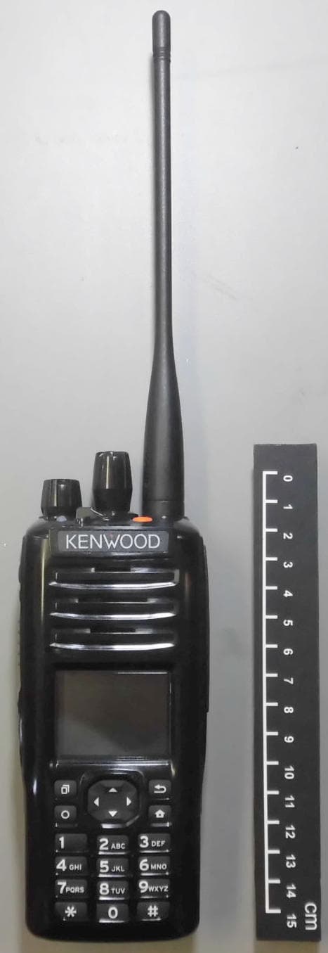
ALH442000
Jul 06, 2014Push to talk radio.
Equipment Class
DXX - Part 15 Low Power Communication Device Transmitter
ALH443801
Dec 09, 2013UHF Digital Transceiver
Equipment Class
TNF - Licensed Non-Broadcast Transmitter Held to Face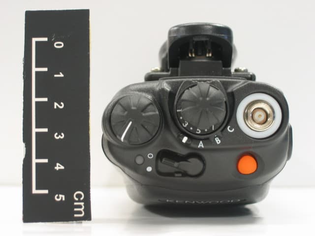
ALH468800
Oct 22, 2013PORTABLE LMR RADIO
Equipment Class
TNF - Licensed Non-Broadcast Transmitter Held to Face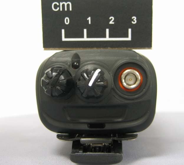
ALH443700
Aug 18, 2013VHF Digital Transceiver Models NX-240-P, NX-240-K, NX-240-M, NX-240-M2, NX-240V-K
Equipment Class
TNF - Licensed Non-Broadcast Transmitter Held to Face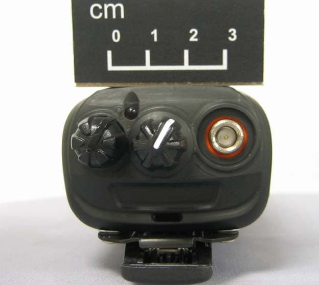
ALH443800
Aug 07, 2013Model NX-340 Digital Transceiver
Equipment Class
TNF - Licensed Non-Broadcast Transmitter Held to Face