ANO12P701XIBM ThinkPad
International Business Machines Corporation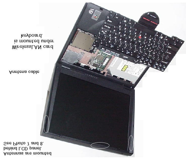
Click to zoom
Application Details
- Equipment Class
- DSS - Part 15 Spread Spectrum Transmitter
- Date of Grant
- Jan 23, 2001
- Application Purpose
- Original Equipment
- Date of Application
- Oct 02, 2000
- Equipment Note
- IBM ThinkPad
- Frequency Range
- 2412.00000000 - 2462.00000000
- Country
- United States
Documents & Files
Document Text
Text extracted from the exhibit documents filed with the FCC. Open a document above to read the original.
Users Manual
Note:Before using this information and the product it supports, be sure to read the general information under “Safety information” on page v, and “Notices” on page 54. First Edition (July 2000) The following paragraph does not apply to the United Kingdom or any country where such provisions are inconsistent with local law: INTERNATIONAL BUSINESS MACHINES CORPORATION PROVIDES THIS PUBLICATION "AS IS" WITHOUT ANY WARRANTY OF ANY KIND, EITHER EXPRESS OR IMPLIED, INCLUDING, BUT NOT LIMITED TO, THE LIMITED WARRANTIES OF MERCHANTABILITY OR FITNESS FOR A PARTICULAR PURPOSE. Some states do not allow disclaimers or express or implied warranties in certain transactions; therefore, this statement may not apply to you. This publication could include technical inaccuracies or typographical errors. Changes are periodically made to the information herein; these changes will be incorporated in new editions of the publication. IBM may make improvements or changes in the products or the programs described in this publication at any time. Requests for technical information about IBM products should be made to your IBM Authorized Dealer or your IBM Marketing Representative. Copyright International Business Machines Corporation 2000. All rights reserved. Note to US Government Users — Documentation related to restricted rights — Use, duplication, or disclosure is subject to restrictions set forth in GSA ADP Schedule Contract with IBM Corp. Contents Safety information . . . . . . . . . . . . . . . . . . . . . . . . . .v Handling the ThinkPad computer................ xiii ThinkPad do not's.......................... xiv ThinkPad do's . . . . . . . . . . . . . . . . . . . . . . . . . . . . .xvii Cleaning your computer....................... xviii Carrying your computer ....................... xix Extending the usefulness of the battery............... xx System overview . . . . . . . . . . . . . . . . . . . . . . . . . . .1 Features . . . . . . . . . . . . . . . . . . . . . . . . . . . . . . . . .2 Specifications . . . . . . . . . . . . . . . . . . . . . . . . . . . . . .4 Using your online user's guide .................... 6 Starting the BIOS Setup Utility.................... 7 Protecting your computer...................... 9 Using passwords . . . . . . . . . . . . . . . . . . . . . . . . . . .10 Power-on password . . . . . . . . . . . . . . . . . . . . . . . .10 Screen-saver password . . . . . . . . . . . . . . . . . . . . .10 Hard-disk password . . . . . . . . . . . . . . . . . . . . . . . .11 Windows password . . . . . . . . . . . . . . . . . . . . . . . .11 Setup password . . . . . . . . . . . . . . . . . . . . . . . . . .12 Network password . . . . . . . . . . . . . . . . . . . . . . . . .12 Using locks . . . . . . . . . . . . . . . . . . . . . . . . . . . . . .13 Solving computer problems ................... 15 Replacing the hard disk drive .................... 16 Troubleshooting . . . . . . . . . . . . . . . . . . . . . . . . . . . .18 Error codes or messages.................... 18 Errors without codes or messages............... 20 Input problems . . . . . . . . . . . . . . . . . . . . . . . . . . .21 Battery problems . . . . . . . . . . . . . . . . . . . . . . . . .23 Standby or hibernation problems................ 24 Power switch problem ...................... 26 Hard-disk drive problems..................... 27 CD-ROM or DVD-ROM Problems................ 28 Copyright IBM Corporation 2000iii Computer display problems................... 30 Software problems . . . . . . . . . . . . . . . . . . . . . . . .31 Other problems . . . . . . . . . . . . . . . . . . . . . . . . . .32 Testing your computer........................ 33 Backing up your system....................... 34 Backing up your system configuration............. 34 Backing up your data....................... 35 Recovering lost or damaged software ............. 35 Getting service . . . . . . . . . . . . . . . . . . . . . . . . . . . .40 ThinkPad Web site........................ 40 Recording sheets . . . . . . . . . . . . . . . . . . . . . . . . .41 Appendix A. Product warranty and notices .......... 43 Notices . . . . . . . . . . . . . . . . . . . . . . . . . . . . . . . . .54 Year 2000 readiness and instructions............. 54 Trademarks . . . . . . . . . . . . . . . . . . . . . . . . . . . .55 Electronic emission notices ................... 55 Telecommunication notice . . . . . . . . . . . . . . . . . . . .57 Notice for Australia........................ 61 Regions where ThinkPad i Series 1200/1300 has ThinkPad modem integrated . . . . . . . . . . . . . . . . . . . . . . . .61 Notice to New Zealand users of the "Ambit U98.005.C.00 Internal Modem" . . . . . . . . . . . . . . . . . . . . . . . . .62 Notice for European Union countries.............. 63 Index . . . . . . . . . . . . . . . . . . . . . . . . . . . . . . . . . .65 iv v vi Safety information DANGER Electrical current from power, telephone, and communi- cation cables is hazardous. To avoid shock hazard, connect and disconnect cables as shown below when installing, moving, or opening the covers of this product or attached devices. If the 3–pin power cord is provided with this product, it must be used with a properly grounded outlet. Copyright IBM Corporation 2000vii To Connect Turn everything OFF. First, attach all cables to devices. Attach the signal cables to the receptacles. Attach the power cord to an outlet. Turn the device ON. To Disconnect Turn everything OFF. First, remove the power cord from the outlet. Remove the signal cables from the receptacles. Remove all cables from device. viii DANGER Reduce the risk of fire and electric shock by always fol- lowing basic safety precautions, including the following: Do not use your computer in or near water. During electrical storms: – Do not use your computer with the telephone cable connection. – Do not connect the cable to or disconnect it from the telephone outlet on the wall. ix DANGER If the rechargeable battery pack is incorrectl…
Text truncated - open the document above for the full version.
Block Diagram
FCC Test Report FCC ID: ANO12P701X Document Number: FCC-19-0152-0 Prepared by T. Murota and T. Asano 8/43 3. BLOCK DIAGRAM 3.1 Block Diagram of the PC system unit ( IBM ThinkPad i Series 1300) Fig. 2 Block diagram of ThinkPad i 1300 FCC Test Report FCC ID: ANO12P701X Document Number: FCC-19-0152-0 Prepared by T. Murota and T. Asano 9/43 3.2 Block Diagram of the Wireless-LAN mini-PCI card Fig. 3 Block diagram of the Wireless-LAN mini-PCI card
External Photos
FCC Test Report FCC ID: ANO12P701X Document Number: FCC-19-0152-0 Prepared by T. Murota and T. Asano 29/43 11. PHOTOS OF TESTED EUT Photo.1: Front View : IBM ThinkPad i Series 1300 (1171-21U/2AU, 12 inch LCD) Photo.2: Front View : IBM ThinkPad i Series 1300 (1171-71U, 13 inch LCD) FCC Test Report FCC ID: ANO12P701X Document Number: FCC-19-0152-0 Prepared by T. Murota and T. Asano 30/43 Photo.3: Rear View : IBM ThinkPad i Series 1300 (all models) Photo.4: Rear View : Connector terminals FCC Test Report FCC ID: ANO12P701X Document Number: FCC-19-0152-0 Prepared by T. Murota and T. Asano 31/43 Photo.5: Locations of IEEE802.11b Wireless-LAN mini-PCI card and Antenna
ID Label/Location Info
FCC Test Report FCC ID: ANO12P701X Document Number: FCC-19-0152-0 Prepared by T. Murota and T. Asano 7/43 2. PRODUCT LABELING rear side bottom view Fig.1 FCC label of ANO12P701X
Internal Photos
FCC Test Report FCC ID: ANO12P701X Document Number: FCC-19-0152-0 Prepared by T. Murota and T. Asano 32/43 Photo.6: Exterior views of IEEE802.11b Wireless-LAN mini-PCI card FCC Test Report FCC ID: ANO12P701X Document Number: FCC-19-0152-0 Prepared by T. Murota and T. Asano 33/43 Photo.7: Diversity Antennas mounted in LCD IBM ThinkPad i Series 1300 (1171-21U/2AU, 12 inch LCD) FCC Test Report FCC ID: ANO12P701X Document Number: FCC-19-0152-0 Prepared by T. Murota and T. Asano 34/43 Photo.8: Diversity Antennas mounted in LCD IBM ThinkPad i Series 1300 (1171-71U, 13 inch LCD) FCC Test Report FCC ID: ANO12P701X Document Number: FCC-19-0152-0 Prepared by T. Murota and T. Asano 35/43 Photo.9: Exterior views of Antenna
Internal Photos
FCC Test Report FCC ID: ANO12P701X Document Number: FCC-19-0152-1 Prepared by T. Murota 1/2 Attachment-1 Exterior Views of Wireless-LAN Card Top side views of IEEE802.11b Wireless-LAN mini-PCI card With metallic shielding covers Without metallic shielding covers FCC Test Report FCC ID: ANO12P701X Document Number: FCC-19-0152-1 Prepared by T. Murota 2/2 Back side views of IEEE802.11b Wireless-LAN mini-PCI card With metallic shielding covers Without metallic shielding covers
Operational Description
FCC Test Report FCC ID: ANO12P701X Document Number: FCC-19-0152-0 Prepared by T. Murota and T. Asano 10/43 3.3 Description of the Wireless-LAN mini-PCI card The various parts of the Block diagram are numbered and an explanation is given of these blocks. 3.3.1 General RF specifications SpecificationsRelated regulation Attached Refference Peak output power31.6mW (15dBm)Part 15.247.bPage 39(Senton-TP.pdf) center2.412GHzPage 67(Senton-TP.pdf)Lowest (Ch.1) 6db BW2.404GHzPart 15.247.a2 Page 32(Senton-TP.pdf) center2.462GHzPage 75(Senton-TP.pdf) Frequency range Highest (CH.11) 6db BW2.470GHzPart 15.247.a2 Page 38(Senton-TP.pdf) 3.3.2 Transmitter functions A) Digital Signal Processor. (22) Function : Generate spread signal with an Barker sequence of 11, the original raw data rate of two Megabits is transformed to a symbol rate of one MegaBaud and multiplied with eleven and modulated with a DQPSK ( Differential Quadrature Phase Shift Keying ) Modulation. The unfiltered data comes out of I and Q and goes to the up/down mixer (6) B) The above signals are mixed in (6) in a so called quadrature modulator with the Intermediate Frequency (IF) of 352 MHz. C) The upmixer is fed by the VCO of 704 MHz, which is divided by 2 to 352 MHz. D) The SAW ( 8 ) filters all unwanted mixing products, such that only the 352 MHz band remains. E) This signal goes into the RF upmixer (9) SA2420 were it is mixed with the RF VCO with a range of 2050 to 2150 MHz. F) The Rx/Tx switch (17) brings the signal to the variable attenuator (10), where the output level is controlled. G) The signal is fed through a 2.4- 2.5 GHz bandpass filter (11) to remove all unwanted mixer products, and thus to get a clean signal for further processing. H) The signal is amplified in (12), with approx. 23 dB to an output level of approx. 15 dBm I) This signal goes to the special connector. J) The output power is controlled with a so called power feed back loop (15) in which the output power is compared with a DAC value from (10) 3.3.3 Receiver functions K) The receive signal enters the antenna passes the RX/TX switch (14) and (13) this is set to RX mode. L) The signal goes through the 2.4 GHz filter (16) to remove all unwanted spectral components in order to deliver a clean signal for the receiver. M) A Low Noise Amplifiers (LNA) (in 9) is used to amplify the weak signal to a level fitted for down mixing. FCC Test Report FCC ID: ANO12P701X Document Number: FCC-19-0152-0 Prepared by T. Murota and T. Asano 11/43 N) The AGC (27) can amplify or attenuate the signal according to the Digital signal processor required input with a step size of 26 dB. O) Again the Rx/Tx switch in the Rx mode is passed and also the same filter as in transmit mode (18). P) The down mixer (9) mixes the 2.4 GHz with the 2.1 GHz to the 352 MHz IF. Q) The signal of 352 MHz is amplified again (9) and filtered by a SAW filter (19) to give a clean signal for the second mixer. R) The Downmixer (6) mixes the 352 MHz signal down to the I and Q signals, also the auto gain control can increase the level to the required level via line 20. S)The very low amplitude baseband I and Q signal is amplified in the AMPs (6) to a level fitted for the Analogue to Digital converters (22), which make it a proper signal for the digital signal processor. T) The digital signal processor (22) removes the spreading as present on the signal with a so called autocorrelation function. The resulting output of the processor is a received data rate of 2 Megabits. 3.3.4 VCO, PLL and OSC U)These three form one entity to generate a single tone signal for down mixing. There are two of these blocks available, one for the IF LO (7 and 6) (352MHz ) and one for the RF LO (25 and 26) of 2050 to 2150 MHz. V)All the PLL’s and the processor (2) have one reference Crystal of 22 MHz (4) with an accuracy of 25 ppm. 3.3.5 General circuits W)Antenna Diversity. Depending on the signal strength and signal quality the Digital processor (22) can select between two antenna’s which gives the best signal. This is done initial during the training sequence in the received signal. X)Automatic Gain control. Depending on the signal strength and signal quality the Digital processor (22) can choose to increase or decrease the signal level at the digital input, this is done by reducing or increasing the gain in the receiver via the LNA-AGC (in 9). Y) The Signal processor (22) can read via the MAC (2) the registers for programming all Z) The MAC is used to do the handshaking with the miniPCI bridge chip bus (1) and handling the IEEE protocol. Also used to load the PLL frequencies and dividers, also used to interface to the EEPROM which contains all parameters for the PLL’s and the Callcode
Operational Description
Nederland B.V. WCND Report No. 015127, Rev. A TEST REPORT Subject: Processing Gain For the ORiNOCO IEEE802.11b products Ref.: FCC Rules 47 CFR Part 15, Section 5.247d Report Prepared by: Maarten Visee July 28, 2000 NameSignatureDate Concurrence: 1. Director of Engineering Bruce Tuch August 10, 2000 NameSignatureDate 2. Team Captain Frans Hoekstra August 10, 2000 NameSignatureDate Lucent WCND Confidential Information ©2000 FCC Processing Gain Measurements Results, for the OriNOCO IEEE802.11b products, Report No. 015127, Rev. A. Lucent WCND Confidential ©2000 1 This document describes the Receiver Processing Gain verification measurements performed at the WaveLAN-II PC-Card Type 2, according to Ref.[2]. The Lucent WaveLAN-II PC-Card Type 2 product confirms to the minimum required 10 dB processing gain, as set forth by the FCC for operation in the 2.4 GHz ISM band. 1- Document FCC 97-114, Appendix C, Guidance on Measurements for Direct Sequence Spread Spectrum Systems. 2- Hardware Functional Specification for WaveLAN-II Embedded, High Speed, Doc. No. 011735, Rev. A, Source Organization Lucent Technologies WCND Utrecht. 3-Viterbi, A. J., Principles of Coherent Communications, New York, McGraw-Hill 1966. 4- Proakis, J.G., Digital Communications, New York, McGraw-Hill 1989, page 270. 4.1 Test introduction - FCC requirements: Part of FCC certification for the Lucent WaveLAN IEEE 802.11 High Speed compliant Network Interface Card (NIC) is a processing gain test. This test proves that the receiver of the tested product employs a true spread spectrum device receiver structure, taking full advantage of the direct sequence spread spectrum modulation technique. This test verifies the receiver processing gain to be 10 dB or more for a data rate of 1, 2, 5.5 and 11 Mbit/s, by monitoring the Bit Error Rate (BER) of the product under test for each data rate, while operating under strict defined received signal conditions. Several methods of showing compliance to the rules are possible, from a stepped CW jammer to a continuous sweeping CW interferer. For this test the discrete stepped CW jammer method was chosen, as described in Ref.[1]. Therefore a receiver input signal is applied to the product under test, in the presence of a Continuous Wave (CW) interference source, also referred to as CW jammer. 1.Summary: 2.Conclusion: 3.References: 4.Measurement description: FCC Processing Gain Measurements Results, for the OriNOCO IEEE802.11b products, Report No. 015127, Rev. A. Lucent WCND Confidential ©2000 2 The test takes place at the product Functional Specification (Ref.[2]) specified conditions for BER rate measurements, specifying a BER equal or better than 10^-8 at a receiver input level of -55 dBm. For practical reasons these test are performed at -55 dBm or -53 dBm. This small deviation from the Functional Specification should not cause any deviation from the specified Bit Error Rate, since the received levels are well above the thermal noise. The test criteria for meeting the minimal processing gain is such that it takes the theoretical calculated SNR for the applied modulation technique and specified BER as a reference. From this given SNR the processing gain is subtracted, yielding the CW Jammer to Signal ratio J/S. From Ref. [4], likewise as Ref.[3] consulted in Ref. [1], it is determined that for a BER of 10^-8 the SNR (S/N)o equals: 13 dB @ 1 Mbit/s, 15 dB @ 2 Mbit/s, 15 dB @ 5.5 Mbit/s, 18 dB @ 11 Mbit/s. Thus the J/S ratio for a processing gain of 10 dB that must be met is calculated as: -13 + 10 = -3 dB @ 1 Mbit/s (DBPSK), -15 + 10 = -5 dB @ 2 Mbit/s (DQPSK), -15 + 10 = -5 dB @ 5.5 Mbit/s (CCK), -18 + 10 = -8 dB @ 11 Mbit/s (CCK). Two types of measurement corrections are allowed for as described in Ref.[1]. The first taking into account 2 dB implementation losses, thus increasing the absolute J/S ratio by 2 dB. The second correction allows for deleting the 20% worst- case frequencies in the processing gain test that causes the test at that CW interference to fail. This implies that for the considered 14 MHz wide measurement interval the worst case 57 CW jammer frequencies can be ignored, being those that result in received data errors/missing frames (20% of 14 MHz *(1 MHz/50 KHz) + 1 = (20% * 281) + 1 = 57). FCC Processing Gain Measurements Results, for the OriNOCO IEEE802.11b products, Report No. 015127, Rev. A. Lucent WCND Confidential ©2000 3 4.2 Test sequence: The measurements are performed at a 50 KHz CW jammer raster. For each CW jammer frequency 10^8 bits are transmitted by the reference transmitter, and received by the product under test. For practical reasons 50.000 messages are transmitted. After blanking out frame overhead 1927 bits per frame are monitored. This results in 50.000 * 1927 = 9650000 transmitted bits for a BER test, which is a mere 1.4% less than the targeted 10^8 bits. Though it would be more elegant to show BER compliance for at least say ten times 10^8 transmitted/received bits, the time involved with this grows significantly. Since the CW interferer is stepped in a 50 KHz raster, covering the receiver bandwidth of 14 MHz, it is considered that the BER requirement is sufficiently met since such a multitude of measurements are taken. The total measurement is being performed under computer control, hereafter referred to as controller. It involves the control over the reference transmitter, CW-interference generator, receiver under test and received data error- checker/frame counter. The controller is programmed by a configuration file, that lists the CW jammer frequencies and CW jammer signal levels. The controller program flow chart is given in Annex A, WaveLAN-II FCC Processing Gain Measurements, Controller Flow Chart. The transmitted data pattern is fixed, and known at the receiver. Therefore the error checker compares the known transmitted data sequence with received data sequence. Received data errors and missing received frames information is retrieved by the cont…
Text truncated - open the document above for the full version.
Operational Description
FCC Test Report FCC ID: ANO12P701X Document Number: FCC-19-0152-1 Prepared by T. Murota 1/1 Attachment-2 1) Process gain data at 11Mbps and 2Mbps - Tests were performed at Spreading gain 10.4 dB. Engineering took extra margin. - At 11Mbps S/N may be 18 dB, 2Mbps S/N may be 15 dB. - SIR (Signal Interference Ratio) = S/N + Spreading gain + Lsys. (= -Mj) We take only 1 dB Lsys for 11Mb/s or 0 dB Lsys for 2Mb/s into account so that : 11Mbps SIR = 18 dB - 10.4 dB + 1 = 8.6 (round of f upwards to 9) dB = (-)Mj With this 9 dB SIR (= -9 dB Mj) we test unit and check for less than 20% errors (Acutually 18.57%), 2Mbps SIR = 15 dB - 10.4 dB + 0 = 4.6 (round of f upwards to 5 ) dB = (-)Mj With this 5 dB SIR (= -5 dB Mj) we test unit and check for less than 20% errors, (Acutually 3.21%). Thus in principle exact calculations in this case are : Processing gain for 11Mbps = S/N + Mj + Lsys = 18 + (-)8.6 + 1 = 10.4 dB Processing gain for 2Mbps = S/N + Mj + Lsys = 15 + (-)4.6 + 0 = 10.4 dB 2) Chip/symbol rate, the symbol/bit rate and the Chip/bit Bit rateChip/symbol rateBit/symbol rateChip/bit rate 1 Mbit/sec111, DBPSK11 2 Mbit/sec112, DQPSK5.5 5.5 Mbit/sec84, CCK2 11 Mbit/sec88, CCK1 Note) As for how to meet the 10 dB requirement of Processing Gain is explained in 1). Measurement file output name is:2mbit.cnd Input command file name is:INPUT.CMDNote: 2 Mbit, 5 dB SIR tested for (15 dB SNR - 10.4 - 0 impl. losses). Input CW correction level:6dBTakes not into account allowed useage of 2 dB SIR implementation losses margin. Lowcount is:1000messagesAttention: Input the red cells for correct spreadsheet calculations! Highcount is:50000messagestotal errors9 Rx level DUT is:-55dBmpercentage3.21% Number of received data errors as a function of frequency and interference levelOK?=<20%, OK Not measured combinations listed as "-1"HIJKLMNOPQRS Uncorrected Interference level dialed at CW generator -60-59-58-57-56-55-54-53-52RxD ErrorsPDARxD ErrorsPDABoth error True CW interference level at receiver input (dBm)detectedmissingdetectedmissingRxD and -66-65-64-63-62-61-60-59-58full testfull testup to CWup to CWPDA J/S ratio (dB)-11#PDA-10#PDA-9#PDA-8#PDA-7#PDA-6#PDA-5#PDA-4#PDA-3#PDArangerange=< -60 dBm=< -60 dBm=< -60 dBm Frequency (Hz)(J/S = -5 dB)(J/S = -5 dB)time 24090000000100001000010000100001000010000100001000050000OK, 0 RxD errorsOK, No PDA errors0005:14:58 24090500000100001000010000100001000010000100001000050000OK, 0 RxD errorsOK, No PDA errors0005:11:49 24091000000100001000010000100001000010000100001000050000OK, 0 RxD errorsOK, No PDA errors0005:08:41 24091500000100001000010000100001000010000100001000050000OK, 0 RxD errorsOK, No PDA errors0005:05:34 24092000000100001000010000100001000010000100001000050000OK, 0 RxD errorsOK, No PDA errors0005:02:25 24092500000100001000010000100001000010000100001000050000OK, 0 RxD errorsOK, No PDA errors0004:59:17 24093000000100001000010000100001000010000100001000050000OK, 0 RxD errorsOK, No PDA errors0004:56:08 24093500000100001000010000100001000010000100001000050000OK, 0 RxD errorsOK, No PDA errors0004:53:00 24094000000100001000010000100001000010000100001000050000OK, 0 RxD errorsOK, No PDA errors0004:49:52 24094500000100001000010000100001000010000100001000050000OK, 0 RxD errorsOK, No PDA errors0004:46:43 24095000000100001000010000100001000010000100001000050000OK, 0 RxD errorsOK, No PDA errors0004:43:35 24095500000100001000010000100001000010000100001000050000OK, 0 RxD errorsOK, No PDA errors0004:40:26 24096000000100001000010000100001000010000100001000050000OK, 0 RxD errorsOK, No PDA errors0004:37:18 24096500000100001000010000100001000010000100001000050000OK, 0 RxD errorsOK, No PDA errors0004:34:10 24097000000100001000010000100001000010000100001000050000OK, 0 RxD errorsOK, No PDA errors0004:31:01 24097500000100001000010000100001000010000100001000050000OK, 0 RxD errorsOK, No PDA errors0004:27:52 24098000000100001000010000100001000010000100001000050000OK, 0 RxD errorsOK, No PDA errors0004:24:44 24098500000100001000010000100001000010000100001000050000OK, 0 RxD errorsOK, No PDA errors0004:21:35 24099000000100001000010000100001000010000100001000050000OK, 0 RxD errorsOK, No PDA errors0004:18:27 24099500000100001000010000100001000010000100001000050000OK, 0 RxD errorsOK, No PDA errors0004:15:18 24100000000100001000010000100001000010000100001000050000OK, 0 RxD errorsOK, No PDA errors0004:12:10 24100500000100001000010000100001000010000100001000050000OK, 0 RxD errorsOK, No PDA errors0004:09:01 24101000000100001000010000100001000010000100001000050000OK, 0 RxD errorsOK, No PDA errors0004:05:53 24101500000100001000010000100001000010000100001000050000OK, 0 RxD errorsOK, No PDA errors0004:02:44 24102000000100001000010000100001000010000100001000050000OK, 0 RxD errorsOK, No PDA errors0003:59:36 24102500000100001000010000100001000010000100001000050000OK, 0 RxD errorsOK, No PDA errors0003:56:27 24103000000100001000010000100001000010000100001000050000OK, 0 RxD errorsOK, No PDA errors0003:53:19 24103500000100001000010000100001000010000100001000050000OK, 0 RxD errorsOK, No PDA errors0003:50:11 24104000000100001000010000100001000010000100001000050000OK, 0 RxD errorsOK, No PDA errors0003:47:02 24104500000100001000010000100001000010000100001000050000OK, 0 RxD errorsOK, No PDA errors0003:43:54 24105000000100001000010000100001000010000100001000050000OK, 0 RxD errorsOK, No PDA errors0003:40:46 24105500000100001000010000100001000010000100001000050000OK, 0 RxD errorsOK, No PDA errors0003:37:37 24106000000100001000010000100001000010000100001000050000OK, 0 RxD errorsOK, No PDA errors0003:34:28 24106500000100001000010000100001000010000100001000050000OK, 0 RxD errorsOK, No PDA errors0003:31:20 24107000000100001000010000100001000010000100001000050000OK, 0 RxD errorsOK, No PDA errors0003:28:11 24107500000100001000010000100001000010000100001000050000OK, 0 RxD errorsOK, No PDA errors0003:25:03 24108000000100001000010000100001000010000100001000050000OK, 0 RxD errorsOK, No PDA errors0003:21:54 24108500000100001000010000…
Text truncated - open the document above for the full version.
RF Exposure Info
FCC Test Report FCC ID: ANO12P701X Document Number: FCC-19-0152-1 Prepared by T. Murota 1/1 Attachment-4 RF Exposure The specification of RF conducted output power is 15dBm, and the antenna gain is 5.2dBi. Therefore this applying product (FCC ID : ANO12P701X) is a low power wireless equipment with 20.2dBm(105mW). According to the definition of FCC Part 2.1091, the applying equipment should be classified as a mobile device in that normal usage results in more than 20cm separation between user and antenna. And the Maximum Permissible Exposure(MPE) shown in 47 CFR 1.1310 is 1mW/cm 2 for 2.4GHz band. Using the above values (RF power and MPE), the minimum distance(R) from the antenna for the allowed MPE limit is calculated with the following formula. Namely, 3 cm is the minimum safety distance for human exposure to radio frequency(RF) electromagnetic energy from the antenna of this equipment. Generally users operate this equipment with a sufficient distance greater than 20 cm from the antenna during a normal operation. Though a user can operate within 3 cm of distance, an extraordinary posture will be necessary. And there is no inevitability for the user to do so. Therefore the applying equipment fairly meets the RF exposure requirement under almost operation in ordinary state. Antenna position
RF Exposure Info
FCC Test Report FCC ID: ANO12P701X Document Number: FCC-19-0152-1 Prepared by T. Murota Attachment-4 RF Exposure SP(1): The peak conducted output power of the applying equipment is 15 dBm (P = 31.6mW). This measurement was performed at the maximum condition with CW(continuous wave) as shown below. So the source-based time-averaging duty factor is considered as 100% duty. FCC Test Report FCC ID: ANO12P701X Document Number: FCC-19-0152-1 Prepared by T. Murota And the peak radiated (EIRP) output power is calculated as follows. Therefore this applying equipment is classified as the Transmitter Category V), Part 15 Fixed and Mobile Transmitters, Section F. SP(3): In line with the instruction of Section F, the users notification shown in the next page is delivered to customers associated with the users manual. But the wording is adapted accordingly, since the antenna of the equipment is not installable by users. SP(5): The applying equipment has 11 channels, but it selects one of the available frequencies in the link establishing phase in line with the standard CCA procedure of IEEE802.11b, then starts radiocommunication in a single frequency band. SP(7): Not applicable, since the antenna of the applying equipment is not installable nor detachable by users. SP(8): The document refered to SP(3) indicates the operating instructions of which conditions are for satisfying FCC RF exposure compliance. AS to the installation instructions, it’s not applicable for the equipment as mentioned in SP(7). FCC Test Report FCC ID: ANO12P701X Document Number: FCC-19-0152-1 Prepared by T. Murota Exposure to Radio Frequency Energy Part Number : xxxxxxx IMPORTANT NOTE To comply with FCC RF exposure compliance requirements, a separation distance of at least 20 cm (8 inches) must be maintained between the antenna of this device and all persons. Antenna position
RF Exposure Info
Exposure to Radio Frequency Energy Part Number : xxxxxxx IMPORTANT NOTE To comply with FCC RF exposure compliance requirements, a separation distance of at least 20 cm (8 inches) must be maintained between the antenna of this device and all persons. Antenna position FCC Certification of this device prohibits the use of any other Radio Frequency wireless device in conjunction with your ThinkPad i Series notebook wireless LAN. Do not use any wireless PCMCIA card in your ThinkPad i Series notebook while operating the internal wireless LAN function. Furthermore, any tampering of the internal antenna will void the FCC Certification and your warranty.
Test Report
FCC Test Report FCC ID: ANO12P701X Document Number: FCC-19-0152-0 MEASUREMENT/TECHNICAL REPORT – Part 15 Subpart C (Intentional Radiator) IBM ThinkPad i Series 1300 (1171-21U/2AU/71U) FCC ID : ANO12P701X September 4, 2000 This report concerns: (check one) Original Grant ̧ Class I change Class II change Equipment type: Wireless LAN device in Computer (computer, printer, modem, etc.) This report shall not be reproduced except in full, without the written permission of this test lab. The measurement results contained in this report relate only to the item which was tested. Measurement procedure used is ANSI C63.4-1992 unless otherwise specified. Other test procedure: The FCC has issued provisional acceptance of this test laboratory for Declaration of Conformity testing per letter dated 1997. APPLICANT ANTI-DRUG ABUSE CERTIFICATION: By checking yes, the applicant certifies that, in the case of an individual applicant, he or she is not subject to a den…
Text truncated - open the document above for the full version.
Contact Information
Applicant
John Maas(Corp Program Manager EMC)
Technical Contact
IBM Japan Ltd.Takeshi Asano
[email protected]81 46 215 4779
1623-14 Shimotsuruma Yamato-shi · Yamato-shi · Japan
Non-Technical Contact
IBM Japan Ltd.Toshiya Murota
[email protected]81 46 215 6574
Test Firm
TUV SUD Product Service GmbH PS-EMC-STRRainer Heller
Technical Specifications
| # | Rule Parts | Frequency Range | Power Output |
|---|---|---|---|
| 1 | 15C | 2.41 GHz - 2.46 GHz | 31.60 mW |
Other Applications from International Business Machines Corporation

ANO-7054SC
Jun 30, 2005Bluetooth Enabled Handheld Scanner
Equipment Class
DSS - Part 15 Spread Spectrum Transmitter
ANO-7054
Jun 28, 2005Model 7054 Mobile Tablet
Equipment Class
DTS - Digital Transmission System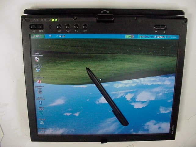
ANOX41T
May 02, 2005ThinkPad X41 Tablet Series
Equipment Class
DCD - Part 15 Low Power Transmitter Below 1705 kHz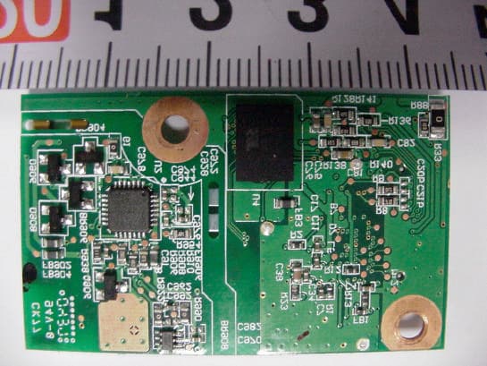
ANO20040700HER
Dec 08, 2004Model: J07M067 Bluetooth Standard Class 2 Adapter
Equipment Class
DSS - Part 15 Spread Spectrum Transmitter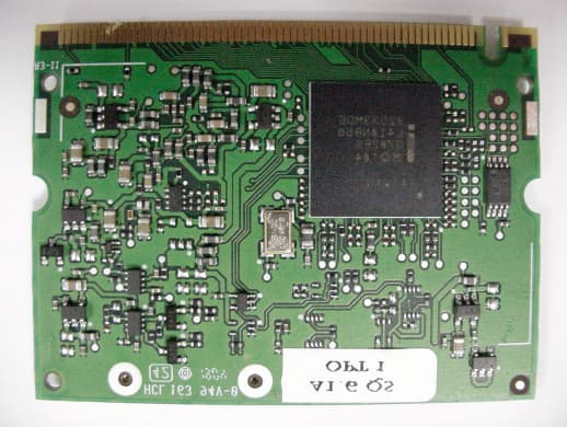
ANO20040601CX2
Oct 06, 2004Model: WM3B2915ABG (802.11a/b/g WLAN Adapter)
Equipment Class
DTS - Digital Transmission System