AQZ-VSR-4141-001differential GPS ground station transmitter
Harris Corporation RF Communications Division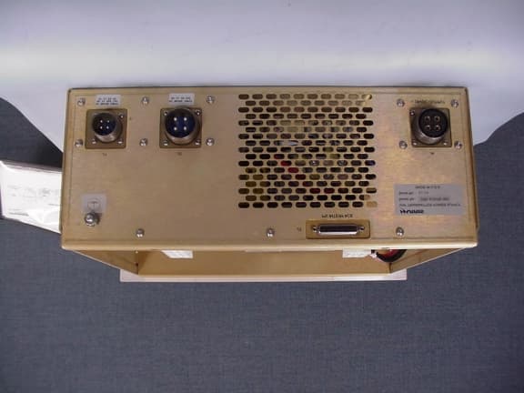
Click to zoom
Application Details
- Equipment Class
- TNB - Licensed Non-Broadcast Station Transmitter
- Date of Grant
- Apr 04, 2001
- Application Purpose
- Original Equipment
- Date of Application
- Aug 14, 2000
- Equipment Note
- differential GPS ground station transmitter
- Frequency Range
- 112.00000000 - 117.95000000
- Country
- United States
Documents & Files
Document Text
Text extracted from the exhibit documents filed with the FCC. Open a document above to read the original.
Users Manual
Attachment to FCC Form 731 FCC ID: AQZ-VSR-4141-001 Exhibit 8 TX Operate Instructions Paragraph 2.1033(c)3 The full contents of Exhibit 8 are contained in 2 files as follows: 1. File 1: this header sheet 2. File 2: an electronic copy of the document: LAAS Host Simulator User Manual. The SCAT VHF Transmitter, model number VSR-4141-001, referenced in this application for certification, has exactly the same hardware as the LAAS VHF Transmitter, model number VLR-4141- 001, referenced in this document. The installed software differs slightly between the two units, solely due to the slight modulation waveform differences between the two, the control of the output power level, and the somewhat narrower frequency range for the SCAT Transmitter, VSR-4141-001. The information contained herein is applicable to both model numbers.
Users Manual
Document Number/Ref.-No.Issue 00-6383A011.0 (113491 2) Page 1 of 26 Copyright 2000 by Harris Corporation, RF Communications Division All rights reserved. No part of this publication may be reproduced or transmitted in any form or by any means, electronic or mechanical, including photocopy, recording, or any information storage and retrieval system, without permission in writing by Harris Corporation, RF Communications Division, Rochester, New York, USA Document Title: LAAS Host Simulator User Manual Document Approval Project Manager Name: J. Lundberg Date and Signature Process Approvals SQA ManagerATC CM ManagerATC SW ManagerATC Dir. Of Ops. Name: D. Kavanagh Name: B. Roeder Name: R. Gray Name: J. Sternowski Date and SignatureDate and SignatureDate and SignatureDate and Signature Document Number/Ref.-No.Issue 00-6383A011.0 (113491 2) Page 2 of 26 Copyright 2000 by Harris Corporation, RF Communications Division All rights reserved. No part of this publication may be reproduced or transmitted in any form or by any means, electronic or mechanical, including photocopy, recording, or any information storage and retrieval system, without permission in writing by Harris Corporation, RF Communications Division, Rochester, New York, USA Change History Issue Change ID DescriptionDateAuthor/Signature 1.0Initial Release09 June 2000D. Hoppe Document Number/Ref.-No.Issue 00-6383A011.0 (113491 2) Page 3 of 26 Copyright 2000 by Harris Corporation, RF Communications Division All rights reserved. No part of this publication may be reproduced or transmitted in any form or by any means, electronic or mechanical, including photocopy, recording, or any information storage and retrieval system, without permission in writing by Harris Corporation, RF Communications Division, Rochester, New York, USA TABLE OF CONTENTS 1INTRODUCTION4 1.1P URPOSE 4 1.2S COPE 4 1.3S YS TE M O VERVIEW 4 1.4D OCUMENT O VERVIEW 4 2APPLICABLE DOCUMENTS6 2.1G OVERNMENT D OCUMENTS 6 2.2N ON -G OVERNMENT D OCUMENTS 6 2.3H ARRIS C ORPORATION RF C OMMUNICATIONS D IV IS ION D OCUMENTS 7 3LAAS HOST SIMULATOR HARDWARE REQUIREMENTS8 3.1PC S YS TE M R EQUIREMENTS 8 3.2C OMPUTER B OARDS CIO-CTR05 C OUNTER I/O ISA CARD 8 3.3I NTERFACE B OX 8 4OPERATION OF THE LAAS HOST SIMULATOR9 4.1C ONNECTING LAAS R ECEIVER AND LAAS T RANSMITTER TO LAAS H OST S IMUL A TOR PC9 4.2F IL E P LACEMENT 10 4.3H OW TO CONFIGURE AND EXECUTE THE LAAS H OST S IMUL A TOR 10 4.3.1Installing the Counter I/O ISA card10 4.3.2Determining if the Counter I/O ISA card is properly installed10 4.3.3Determining if the LAAS Host Simulator can communicate with the LAAS radios11 4.4C ALIBRATING C OUNTER I/O ISA CARD 11 4.5E XPLANATION OF C OLLECTING B LOCK F AILURE R ATE S TATISTICS TO A F IL E C OMMAND 12 5ALPHABETICAL LISTING OF ACRONYMS AND ABBREVIATIONS14 List of Appendices Appendix A Help File Text................................................................................................................................. 15 Appendix B HOSTLAAS.CFG file / description of entries..................................................................................... 24 Appendix C Adapter for LAAS Extended Sensitivity Receiver............................................................................... 25 Appendix D Connecting LHS to LAAS receiver and LAAS transmitter..................................................................... 26 Document Number/Ref.-No.Issue 00-6383A011.0 (113491 2) Page 4 of 26 Copyright 2000 by Harris Corporation, RF Communications Division All rights reserved. No part of this publication may be reproduced or transmitted in any form or by any means, electronic or mechanical, including photocopy, recording, or any information storage and retrieval system, without permission in writing by Harris Corporation, RF Communications Division, Rochester, New York, USA 1 Introduction 1.1 Purpose The purpose of this document is to describe how to setup the Local Area Augmentation System (LAAS) Host Simulator (LHS). The additional purpose of this document is to provide a brief description of how to operate the LAAS Host Simulator. The LAAS Host Simulator will also be referred to as LHS. 1.2 Scope The LAAS Host Simulator User Manual describes the requirements for the Personal Computer (PC) used to control a LAAS receiver and a LAAS transmitter. This document also describes how to configure the ComputerBoards, Inc. CIO-CTR05 Counter I/O ISA card. In addition this document provides a brief description of how to operate the LHS. 1.3 System Overview The LAAS Host Simulator system consists of the following equipment: • Intel compatible PC with monitor, keyboard, and two serial ports • A ComputerBoards, Inc. CIO-CTR05 Counter I/O ISA card that plugs into the PC bus • Any of the following receiver/transmitter configurations: • One LAAS transmitter • One LAAS receiver • One LAAS receiver and one LAAS transmitter • Interface Box with power supply • Shielded RS-232 cables to connect LHS PC to Interface Box and shielded RS-232 cables to connect Interface Box to a LAAS receiver and a LAAS transmitter The LHS is used to demonstrate that a LAAS receiver and a LAAS transmitter can be commanded by and report status to a controlling PC. In addition the LHS is used to demonstrate that LAAS messages can be transmitted in various time slots and received and reported to the controlling PC. 1.4 Document Overview This document is comprised of 5 major sections including: an introduction to the document, a list of referenced documents, a description of the hardware needed for operation of the LAAS Host Simulator, a description of how to operate and how to configure the LAAS Host Simulator, and a list of acronyms and abbreviations. The Introduction section provides a general overview of this document and the LAAS Host Simulator. The Applicable Documents section provides a reference list of documents that provide supporting information to the contents of this document. The Hardware Requi…
Text truncated - open the document above for the full version.
Attestation Statements
Attachment to FCC Form 731 FCC ID: AQZ-VSR-4141-001 Exhibit 2 TX Attestation Statement This is to certify that: All data presented herein was taken by a qualified person under my supervision; The equipment upon which all tests were performed is representative of final production units; The equipment tested was found to comply with the applicable requirements of FCC Rule Part 87; To the best of my knowledge and belief, the facts set forth herein are true and correct. John V. Lundberg Sr. Engineering Manager Harris Corporation RF Communications Division
Block Diagram
Proprietary Information. N o part of this publication may be reproduced or transmitted in any for m or by any means , electronic or mechanica l, inc luding p hotocopy, recording, or any inf ormat ion stora ge and retrieva l syste m, w it hout permiss ion in wr it ing by Harris Corporation, RF Communications Division, Rochester, New York, USA Attachment to FCC Form 731 FCC ID: AQZ-VSR-4141-001 Exhibit 4 TX Block Diagrams Part of Paragraph 2.1033(c)10 Proprietary Information. N o part of this publication may be reproduced or transmitted in any for m or by any means , electronic or mechanica l, inc luding p hotocopy, recording, or any inf ormat ion stora ge and retrieva l syste m, w it hout permiss ion in wr it ing by Harris Corporation, RF Communications Division, Rochester, New York, USA Synthesizer I\Q Modulator Attenuators Codec DSP Gate Pre- Driver Lock Detect Freq. Control VCO Enable Exciter Keyline Power Control Tx Enable Vcont: 0-5 VDC = 6-24 dB Attn Vf 112.000- 117.950 MHz, Pwr Out = 20W avg. VfwdVref Directional Coupler BLOCK DIAGRAM, VHF TRANSMITTER, VSR-4141-001 Temperature SensorPS Fan FaultPS Fan Status - on / offDC input MonitorAC Line Monitor+28 VDC Monitor +5 VDC Monitor RS 422 Converters Integrator Maintenance Enable Switch Power Supply heatsink +5 VDC Power Supply Temp Sensor Power Amplifier Assy +28 VDC +28 VDC AC Line Microprocessor Serial Data Communications and GPS Time Sync Pulses PA Fan Control PA Fan Status & Control AC or DC Mains Select + 12 VDC Power Supply +12 VDC Monitor Driver KeylinePA Keyline Driver x3 PA x3 Vr LPF\Coupler Assy Exciter/Amplifier Proprietary Information. N o part of this publication may be reproduced or transmitted in any for m or by any means , electronic or mechanica l, inc luding p hotocopy, recording, or any inf ormat ion stora ge and retrieva l syste m, w it hout permiss ion in wr it ing by Harris Corporation, RF Communications Division, Rochester, New York, USA DDS U11 PLL U55 LPF LPF VCO Q7, Q8, D38 Balanced Modulator U5 Q9,Q10 Transformer T8 Digital Potentiometer U30 14.745 MHz 2.2400 - 2.359 MHz TCXO 112.000 - 117.950 MHz, -10 dBm ModulatedRF Output - 18 dBm IQ Ref Lock Detector U54 Microprocessor Control BLOCK DIAGRAM, VHF TRANSMITTER, SYNTHESIZER Proprietary Information. N o part of this publication may be reproduced or transmitted in any for m or by any means , electronic or mechanica l, inc luding p hotocopy, recording, or any inf ormat ion stora ge and retrieva l syste m, w it hout permiss ion in wr it ing by Harris Corporation, RF Communications Division, Rochester, New York, USA MRF275MRF275 90 0 0 90 MRF183 Transmision Line Matching Transmision Line Matching Transmision Line Matching Transmision Line Matching Quad Coupler -.3 dB IL Quad Coupler-.3 dB IL MRF275MRF275 90 0 0 90 MRF183 Transmision Line Matching Transmision Line Matching Transmision Line Matching Transmision Line Matching Quad Coupler Quad Coupler MRF275MRF275 90 0 0 90 MRF183 Transmision Line Matching Transmision Line Matching Transmision Line Matching Transmision Line Matching Quad Coupler Quad Coupler Quadrature 3 Way Coupler 0 -90 90 Quadrature 3 Way Coupler 0 -90 90 -.2 dB IL Hybrid LPF Fc 108 118 2 Fc 80 dB .2 dB IL Vr Vf Stripline Directional Coupler .2 dB IL 30 dB Directivity 23 dB Coupling 20 Watt D8PSK Ave Power (46 W pk) into 2:1 VSWR 25.7 W ave 59 W pk (includes .2 dB cabling loss and 2: 1 VSWR excess power ) -.8 dB IL 10 W ave 23.6 W pk 5.6 W ave 13 W pk 5.6 W ave 13 W pk +14 dB +23 dB 0.23 W ave 0.51 W pk 0.23 W ave 0.51 W pk 0.5 W ave 1.1 W pk 2.7 mW ave 6 mW pk 2.7 mW ave 6 mW pk 2.7 mW ave 6 mW pk -.8 dB IL 9.6 mW ave 22 mW pk MRF1508 14 dB (on Exciter pwb) -4.3 dBm ave -0.6 dBm pk 10 W ave 23.6 W pk 10 W ave 23.6 W pk 20 WATT D8PSK TRANSMITTER RF POWER TRAIN
Cover Letter(s)
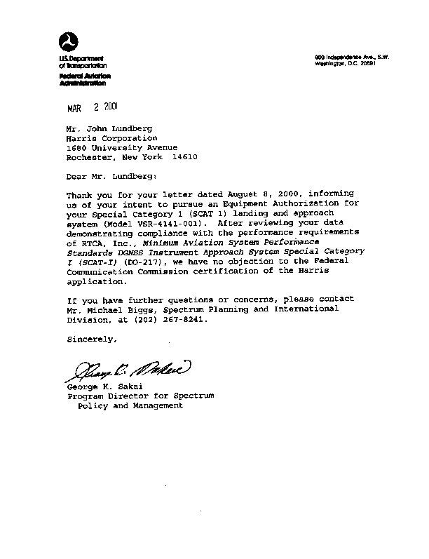
Attachment to FCC Form 731 FCC ID: AQZ-VSR-4141-001 Exhibit 13 Cover Letter The other file in this exhibit includes scanned images of a letter and accompanying information sent to the Federal Aviation Administration on August 8, 2000, in accordance with § 87.147(d) of the FCC Rules.
External Photos
Attachment to FCC Form 731 FCC ID: AQZ-VSR-4141-001 Exhibit 3 VHF Transmitter External Photos Part of Paragraph 2.1033(c)12 External photos are included for both components of the VSR-4141-001 VHF Transmitter: the VSR-4141PA-001 Power Amplifier and the VSR-4141PS-001 Power Supply. The full contents of Exhibit 3 are contained in 2 files as follows: 1. File 1: Full views of the front, rear and sides, for each transmitter component. 2. File 2: Detailed views of the rear of each transmitter component, depicting the ID label details, the relative placement of the ID label and the connectors. Attachment to FCC Form 731FCC ID AQZ-VSR-4141-001 Exhibit 3 External Photographs Tra ns mitte r Powe r Amp lifie r Front View Attachment to FCC Form 731FCC ID AQZ-VSR-4141-001 Exhibit 3 External Photographs Tra ns mitte r Powe r Amp lifie r Le ft V iew Attachment to FCC Form 731FCC ID AQZ-VSR-4141-001 Exhibit 3 External Photographs Tra ns mitte r Powe r Amp lifie r Right View Attachment to FCC Form 731FCC ID AQZ-VSR-4141-001 Exhibit 3 External Photographs Tra ns mitte r Powe r Amp lifie r Rear View Attachment to FCC Form 731FCC ID AQZ-VSR-4141-001 Exhibit 3 External Photographs Tra ns mitte r Powe r Supp ly Front View Attachment to FCC Form 731FCC ID AQZ-VSR-4141-001 Exhibit 3 External Photographs Tra ns mitte r Powe r Supp ly Le ft V iew Attachment to FCC Form 731FCC ID AQZ-VSR-4141-001 Exhibit 3 External Photographs Tra ns mitte r Powe r Supp ly Right View Attachment to FCC Form 731FCC ID AQZ-VSR-4141-001 Exhibit 3 External Photographs Tra ns mitte r Powe r Supp ly Rear View
External Photos
Attachment to FCC Form 731FCC ID AQZ-VSR-4141-001 Exhibit 3 External Photographs Tra ns mitte r Powe r Amp lifie r Labe l V iew Attachment to FCC Form 731FCC ID AQZ-VSR-4141-001 Exhibit 3 External Photographs Tra ns mitte r Powe r Amp lifie r Labe l V iew VSR-4141PA-001 Attachment to FCC Form 731FCC ID AQZ-VSR-4141-001 Exhibit 3 External Photographs Tra ns mitte r Powe r Amp lifie r Connector View Attachment to FCC Form 731FCC ID AQZ-VSR-4141-001 Exhibit 3 External Photographs Tra ns mitte r Powe r Amp lifie r Connector View VSR - 4141PA - 001 Attachment to FCC Form 731FCC ID AQZ-VSR-4141-001 Exhibit 3 External Photographs Tra ns mitte r Powe r Supp ly Connector View VLR - 4141PS - 001
External Photos
Attachment to FCC Form 731 FCC ID: AQZ-VSR-4141-001 Exhibit 3 VHF Transmitter External Photos Part of Paragraph 2.1033(c)12 External photos are included for both components of the VSR-4141-001 VHF Transmitter: the VSR-4141PA-001 Power Amplifier and the VSR-4141PS-001 Power Supply. The full contents of Exhibit 3 are contained in 2 files as follows: 1. File 1: Full views of the front, rear and sides, for each transmitter component. 2. File 2: Detailed views of the rear of each transmitter component, depicting the ID label details, the relative placement of the ID label and the connectors. Attachment to FCC Form 731FCC ID AQZ-VSR-4141-001 Exhibit 3 External Photographs Tra ns mitte r Powe r Amp lifie r Front View Attachment to FCC Form 731FCC ID AQZ-VSR-4141-001 Exhibit 3 External Photographs Tra ns mitte r Powe r Amp lifie r Le ft V iew Attachment to FCC Form 731FCC ID AQZ-VSR-4141-001 Exhibit 3 External Photographs Tra ns mitte r Powe r Amp lifie r Right View Attachment to FCC Form 731FCC ID AQZ-VSR-4141-001 Exhibit 3 External Photographs Tra ns mitte r Powe r Amp lifie r Rear View Attachment to FCC Form 731FCC ID AQZ-VSR-4141-001 Exhibit 3 External Photographs Tra ns mitte r Powe r Supp ly Front View Attachment to FCC Form 731FCC ID AQZ-VSR-4141-001 Exhibit 3 External Photographs Tra ns mitte r Powe r Supp ly Le ft V iew Attachment to FCC Form 731FCC ID AQZ-VSR-4141-001 Exhibit 3 External Photographs Tra ns mitte r Powe r Supp ly Right View Attachment to FCC Form 731FCC ID AQZ-VSR-4141-001 Exhibit 3 External Photographs Tra ns mitte r Powe r Supp ly Rear View
External Photos
Attachment to FCC Form 731FCC ID AQZ-VSR-4141-001 Exhibit 3 External Photographs Tra ns mitte r Powe r Amp lifie r Labe l V iew Attachment to FCC Form 731FCC ID AQZ-VSR-4141-001 Exhibit 3 External Photographs Tra ns mitte r Powe r Amp lifie r Labe l V iew VSR-4141PA-001 Attachment to FCC Form 731FCC ID AQZ-VSR-4141-001 Exhibit 3 External Photographs Tra ns mitte r Powe r Amp lifie r Connector View Attachment to FCC Form 731FCC ID AQZ-VSR-4141-001 Exhibit 3 External Photographs Tra ns mitte r Powe r Amp lifie r Connector View VSR - 4141PA - 001 Attachment to FCC Form 731FCC ID AQZ-VSR-4141-001 Exhibit 3 External Photographs Tra ns mitte r Powe r Supp ly Connector View VLR - 4141PS - 001
ID Label/Location Info
Attachment to FCC Form 731 FCC ID: AQZ-VSR-4141-001 Exhibit 1 TX ID Label Paragraph 2.1033(c)11 The equipment identification label to be used on the VSR-4141-001 VHF Transmitter is shown below and is actual size. TX FCC ID: AQZ-VSR-4141-001 Made in U.S.A. VHF Transmitter This label will be placed on the rear side of the VSR-4141PA-001 Power Amplifier chassis, near the center. Refer to Exhibit 3, External Photos, for a showing of the exact label location.
ID Label/Location Info
Attachment to FCC Form 731 FCC ID: AQZ-VSR-4141-001 Exhibit 1 TX ID Label Paragraph 2.1033(c)11 The equipment identification label to be used on the VSR-4141-001 VHF Transmitter is shown below and is actual size. TX FCC ID: AQZ-VSR-4141-001 Made in U.S.A. VHF Transmitter This label will be placed on the rear side of the VSR-4141PA-001 Power Amplifier chassis, near the center. Refer to Exhibit 3, External Photos, for a showing of the exact label location.
Internal Photos
Attachment to FCC Form 731 FCC ID: AQZ-VSR-4141-001 Exhibit 9 VHF Transmitter Internal Photos Part of Paragraph 2.1033(c)12 Internal photos are included for both components of the VSR-4141-001 VHF Transmitter: the VSR-4141PA-001 Power Amplifier and the VSR-4141PS-001 Power Supply. Exc iter Board Power Amp lifierBoard Attachment to FCC Form 731FCC ID AQZ-VSR-4141-001 Exhibit 9 Internal Photographs Tra ns mitte r Powe r Amp lifie r Top View Attachment to FCC Form 731FCC ID AQZ-VSR-4141-001 Exhibit 9 Internal Photographs Tra ns mitte r Powe r Amp lifie r Exc iter Asse mb ly To p View Exc iter Asse mb ly Attachment to FCC Form 731FCC ID AQZ-VSR-4141-001 Exhibit 9 Internal Photographs Tra ns mitte r Powe r Amp lifie r Power Amp lifier Board To p View Power Amp lifier Board Attachment to FCC Form 731FCC ID AQZ-VSR-4141-001 Exhibit 9 Internal Photographs Tra ns mitte r Powe r Amp lifie r D ire c t io n a l C o up le r As s e mb ly To p View D ire c t io n a l C o up le r Bo a rd Attachment to FCC Form 731FCC ID AQZ-VSR-4141-001 Exhibit 9 Internal Photographs Tra ns mitte r Powe r Supp ly Top View Contro l Board +28 volt Power Supply AC/DC Ma insAsse mb ly DC OutputFilte r Attachment to FCC Form 731FCC ID AQZ-VSR-4141-001 Exhibit 9 Internal Photographs Tra ns mitte r Powe r Supp ly AC/DC Ma ins Board Top View Attachment to FCC Form 731FCC ID AQZ-VSR-4141-001 Exhibit 9 Internal Photographs Tra ns mitte r Powe r Supp ly DC Outp ut F ilter Board Top View
Operational Description
Proprietary Information. N o part of this publication may be reproduced or transmitted in any for m or by any means , electronic or mechanica l, inc luding photocopy, recording, or any inf ormat ion st orage and retrieva l syste m, w it hout per miss ion in wr it ing by Harris Corporation, RF Communications Division, Roc hester, New York, USA Attachment to FCC Form 731 FCC ID: AQZ-VSR-4141-001 Exhibit 12 TX Operational Description • General Information • Range of Operating Power Values [Paragraph 2.1033(c)6] • Description of Circuitry [Paragraph 2.1033(c)10] • Digital Modulation Description [Paragraph 2.1033(c)13] General Information The Harris Model VSR-4141-001 is designed to be a differential Global Positioning System (GPS) VHF ground station transmitter for use in Special Category I (SCAT-1) landing and approach systems. The VSR-4141-001 VHF Transmitter and the Harris Model VSR-4201-001 VHF Receiver together form a radio data broadcast subsystem. The transmitter transmits differential and high-accuracy precision approach waypoint information to an airborne subsystem in order to support highly accurate and reliable GNSS navigation. The transmitted signal is also received by the VHF Receiver (monitor), which demodulates the signal and reports the messages received to a ground facility differential correction processor. This processor also supplies transmit messages to the transmitter. The transmitter uses time mark pulses to set the timing of the transmitted messages. An external interface diagram of the VHF Transmitter is shown in Figure 1. Proprietary Information. N o part of this publication may be reproduced or transmitted in any for m or by any means , electronic or mechanica l, inc luding photocopy, recording, or any inf ormat ion st orage and retrieva l syste m, w it hout per miss ion in wr it ing by Harris Corporation, RF Communications Division, Roc hester, New York, USA Antenna Interface AC Power DC Power Serial Data Interface Remote Power Control VHF Transmitter RS-422 RS-422 Star Point Ground Front Panel Indicators Power on Tx Fault TCXO Test Point Maintenance Lock-out Switch GPS Time Mark Figure 1: Interface Block Diagram, VHF Transmitter Unit With reference to the block diagrams submitted as Exhibit 4, and the schematic diagrams submitted as Exhibit 5, the VHF Transmitter employs digital microcontrollers that perform all control and modulation waveform synthesis functions. The G7D emission utilizes a differentially encoded, 8 phase shift keyed (D8PSK) modulated signal. Maximum power output, over the 112-117.950 MHz frequency range, is 20 Watts average. The transmitter can be powered either from the AC mains, over the operating voltage range of 85 to 265 VAC, or a nominal 28 VDC. 2.1033(c)6 Range of specific operating power levels, and description of any means provided for variation. The rated transmitter output power is 20 Watts average, with a D8PSK waveform. Power output levels of 17.8 Watts (-0.5 dB) and 15.9 Watts (-1.0 dB) are also selectable. Selection of the output level is solely through the remote control interface. Closed loop power control is used to set and maintain the output level. Proprietary Information. N o part of this publication may be reproduced or transmitted in any for m or by any means , electronic or mechanica l, inc luding photocopy, recording, or any inf ormat ion st orage and retrieva l syste m, w it hout per miss ion in wr it ing by Harris Corporation, RF Communications Division, Roc hester, New York, USA 2.1033(c)10 Description of all circuitry and devices provided for determining and stabilizing frequency, for suppression of spurious radiation, for limiting modulation, and for limiting power. Frequency stabilization The VSR-4141-001 Transmitter uses a temperature compensated crystal oscillator (TCXO) to achieve the required frequency stability over its operating temperature range. The TCXO is located on the Exciter board and is used as a master reference oscillator for all transmitter circuits. The TCXO is purchased as a completed unit and consists of a Colpitts oscillator with varactor- thermistor temperature compensating networks. The TCXO vendor tests and calibrates each unit before shipment to ensure that all specifications are met. The TCXO used in the VSR-4141-001 has a frequency stability of 1 part per million (ppm) over the operational temperature range. It also has a DC control pin which is used as a fine frequency adjust to set the oscillator precisely on frequency and correct for aging drift. Refer to Exhibit 5 for a schematic diagram of the circuit in which the TCXO is operated. Suppression of spurious radiation A low pass filter is used to suppress noise on the audio prior to going to the modulator. A RF high pass filter within the low RF signal level stages of the transmitter is used to suppress out-of-band low frequency RF before going to the higher level RF amplifiers. For higher frequency spurious emissions, the transmitter employs a seventh order elliptic function low pass filter with a cutoff frequency of 155 MHz. This filter is physically located on the Directional Coupler/Low Pass filter board assembly. Electrically, it is in the signal path between the power amplifier and the antenna connector in order to suppress conducted harmonic energy before the antenna port. Refer to Exhibit 5 for the schematic diagram of the low pass filter and its associated circuits. Also please refer to Exhibit 9, Internal Photographs, for pictures showing construction and mounting of the low pass filter. For radiated emissions, the transmitter is packaged inside a sheet metal enclosure. Top and bottom covers are equipped with RF gasketing material to prevent cabinet radiation from exceeding specified limits. Filtering is also used on all input/output connectors to further minimize radiation. Modulation limiting The VSR-4141-001 Transmitter employs a digital signal processor (DSP) integrated circuit which runs firmware signal processing algori…
Text truncated - open the document above for the full version.
Parts List/Tune Up Info
Attachment to FCC Form 731 FCC ID: AQZ-VSR-4141-001 Exhibit 10 TX Tune-Up Information Paragraph 2.1033(c)9 The VSR-4141-001 VHF Transmitter utilizes a solid-state power amplifier chain with wideband matching circuits. These matching circuits are comprised of fixed length transmission line segments which eliminate the need for tuning. The only adjustments provided in the transmit amplifier chain are for setting the bias on the various stages. These adjustments are set at the factory and do not require field adjustment.
Schematics
Attachment to FCC Form 731 FCC ID: AQZ-VSR-4141-001 Exhibit 5 Schematic Diagrams Part of Paragraph 2.1033(c)10 Schematic diagrams are included for all circuits used to determine and stabilize frequency, suppress spurious radiation, limit modulation and limit power. The full contents of Exhibit 5 are contained in 4 files as follows: 1. File 1: this header sheet. 2. File 2: drawing number 12008-1251, for the Exciter pwb. 3. File 3: drawing number 12008-1551, for the Directional Coupler/LPF assembly. 4. File 4: drawing number 12008-1651, for the Power Amplifier assembly. The 20 Watt SCAT VHF Transmitter, model number VSR-4141-001, referenced in this application for certification, has exactly the same hardware as the 150 Watt LAAS VHF Transmitter, model number VLR-4141-001. The installed software differs slightly between the two units, solely due to the slight modulation waveform differences between the two, the control of the output power level, and the somewhat narrower frequency range of the SCAT Transmitter, VSR-4141-001. The schematic diagrams included in this exhibit are applicable to both model numbers, but may occasionally reference the higher power levels of the LAAS Transmitter, VLR-4141-001.
Schematics
Attachment to FCC Form 731 FCC ID: AQZ-VSR-4141-001 Exhibit 5 Schematic Diagrams Part of Paragraph 2.1033(c)10 Schematic diagrams are included for all circuits used to determine and stabilize frequency, suppress spurious radiation, limit modulation and limit power. The full contents of Exhibit 5 are contained in 4 files as follows: 1. File 1: this header sheet. 2. File 2: drawing number 12008-1251, for the Exciter pwb. 3. File 3: drawing number 12008-1551, for the Directional Coupler/LPF assembly. 4. File 4: drawing number 12008-1651, for the Power Amplifier assembly. The 20 Watt SCAT VHF Transmitter, model number VSR-4141-001, referenced in this application for certification, has exactly the same hardware as the 150 Watt LAAS VHF Transmitter, model number VLR-4141-001. The installed software differs slightly between the two units, solely due to the slight modulation waveform differences between the two, the control of the output power level, and the somewhat narrower frequency range of the SCAT Transmitter, VSR-4141-001. The schematic diagrams included in this exhibit are applicable to both model numbers, but may occasionally reference the higher power levels of the LAAS Transmitter, VLR-4141-001.
Test Report
Attachment to FCC Form 731 FCC ID: AQZ-VSR-4141-001 Exhibit 6 TX Test Report • FCC Form 731 Submittal Matrix • Final Stages DC Voltages/Currents [Paragraph 2.1033(c)8] • TX Test Report [Paragraph 2.1033(c)14] The full contents of Exhibit 6 are contained in 4 files as follows: 1. File 1: this header sheet, including: • a submittal matrix for the Form 731 attachments (exhibits) vs. the FCC Part 2 requirements for the SCAT VHF Transmitter, Harris model number VSR-4141-001; • DC voltages and currents for the final amplifying stages; • the main portion of the transmitter test report. 2. File 2: Power Output procedure and data 3. File 3: Occupied Bandwidth procedure and data 4. File 4: Frequency Stability procedure and data The SCAT VHF Transmitter, model number VSR-4141-001, referenced in this application for certification, has exactly the same hardware as the LAAS VHF Transmitter, model number VLR-4141-001. The installed software differs slightly between the two units, solely due to the slight modulation waveform differences between the two, the control of the output power level, and the somewhat narrower frequency range of the SCAT Transmitter, VSR-4141-001. Any test data in this report that references the LAAS Transmitter is applicable to both model numbers, unless otherwise so noted. SUBMITTAL MATRIX Part 2 Requirement (Paragraph) DescriptionFiling Submittal 2.1033(c)1Name/mailing addressForm 731 2.1033(c)2FCC IdentifierForm 731 2.1033(c)3Operating InstructionsExhibit 8 2.1033(c)4Emission TypeForm 731 2.1033(c)5Frequency RangeForm 731 2.1033(c)6Operating Power LevelsPart of Exhibit 12 2.1033(c)7Maximum Power RatingForm 731 2.1033(c)8Final Stage DC Voltages/Currents Part of Exhibit 6 2.1033(c)9Tune-Up ProcedureExhibit 10 2.1033(c)10Circuit DetailsExhibits 4 (block diagrams), 5 (schematics), and part of 12 (description) 2.1033(c)11ID LabelExhibit 1 2.1033(c)12PhotographsExhibits 3 (external) and 9 (inter nal) 2.1033(c)13Modulation DescriptionPart of Exhibit 12 2.1033(c)14Test ReportPart of Exhibit 6 2.1033(c)15Part 97 Power AmplifierNot applicable 2.1033(c)16AM Broadcast Stereo Exciter- Generator Not applicable 2.1033(c)17Single ApplicationNot applicable Attestation StatementExhibit 2 Test Setup PhotosExhibit 7 Cover LetterExhibit 13 2.1033(c)8 DC voltages and currents into the final amplifier stages Refer to Exhibit 4, Block Diagrams, and Exhibit 5, Schematic Diagrams, for further details about the Exciter and Power Amplifier PWB assemblies. A summary of the DC power input to the transmit amplifier devices (at 20 watt RF output level) is as follows: DC Voltages and Currents (20 Watt RF power level) PredriverDriverOut…
Text truncated - open the document above for the full version.
Contact Information
Applicant
Thomas Camper, Jr.(Regulatory Manager)
Technical Contact
Harris CorporationDavid F Snyder
[email protected]716-242-3126
RF Communications Division · Rochester, New York · United States
Technical Specifications
| # | Rule Parts | Frequency Range | Power Output | Emission | Tolerance |
|---|---|---|---|---|---|
| 1 | 87 | 112 MHz - 117.95 MHz | 20 W | 14K0G7D | 2.0000000000 ppm |
Other Applications from Harris Corporation RF Communications Division

AQZ-RF-7800W-RPG2
Feb 02, 2020The device is to be used in fixed and nomadic infrastructure for Ethernet data backhaul.
Equipment Class
NII - Unlicensed National Information Infrastructure TXAQZ-RF-7800W-G2
Dec 19, 2015For use in fixed and nomadic infrastructure for Ethernet data backhaul.
Equipment Class
NII - Unlicensed National Information Infrastructure TX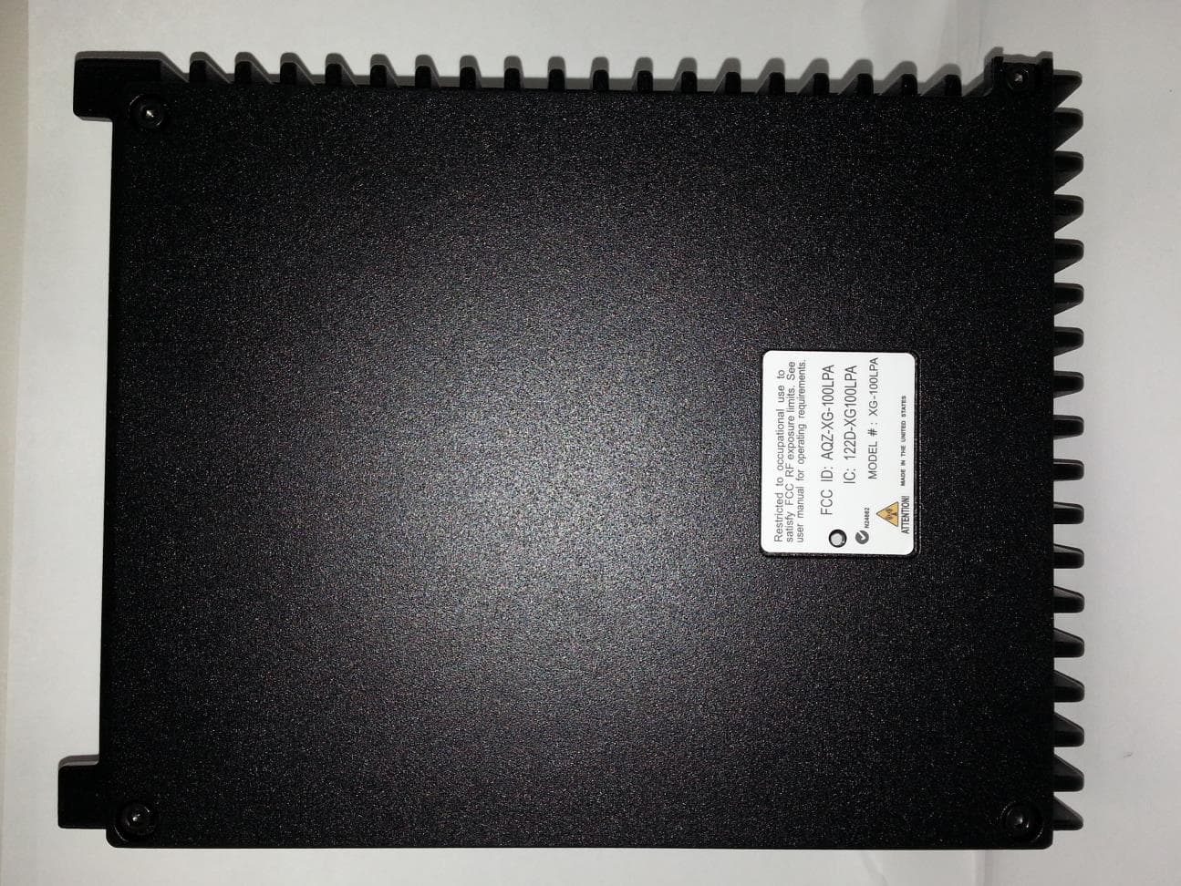
AQZ-XG-100LPA
Feb 09, 2015XG-100LPA Low Band Power Amplifier
Equipment Class
TNB - Licensed Non-Broadcast Station Transmitter
AQZ-12131-1000
Feb 26, 2013Tablet Display Unit
Equipment Class
DSS - Part 15 Spread Spectrum Transmitter
AQZ-XG-100M00
May 23, 2011Unity MultiBand Mobile
Equipment Class
DSS - Part 15 Spread Spectrum Transmitter