ASIV2T001USB wireless transmitter
JVC KENWOOD Corporation
Click to zoom
Application Details
- Equipment Class
- DTS - Digital Transmission System
- Date of Grant
- Apr 10, 2005
- Application Purpose
- Original Equipment
- Date of Application
- Apr 10, 2005
- Equipment Note
- USB wireless transmitter
- Frequency Range
- 2412.00000000 - 2472.00000000
- Company
- JVC KENWOOD Corporation
- Country
- Japan
Documents & Files
Document Text
Text extracted from the exhibit documents filed with the FCC. Open a document above to read the original.
Users Manual
Warnings, Cautions, and Others Mises en garde, précautions et indications diverses Caution–– STANDBY/ON button! Disconnect the mains plug to shut the power off completely. The STANDBY/ON button in any position does not disconnect the mains line. The power can be remote controlled. Attention—Touche STANDBY/ON! Déconnectez la fiche d’alimentation secteur pour couper l’alimentation complètement. La touche STANDBY/ON, dans n’importe quelle position, ne déconnecte pas le système du secteur. L’alimentation ne peut pas être télécommandé. CAUTION To reduce the risk of electrical shocks, fire, etc.: 1. Do not remove screws, covers or cabinet. 2. Do not expose this appliance to rain or moisture. ATTENTION Afin d’éviter tout risque d’électrocution, d’incendie, etc.: 1. Ne pas enlever les vis ni les panneaux et ne pas ouvrir le coffret de l’appareil. 2. Ne pas exposer l’appareil à la pluie ni à l’humidité. WARNING: TO REDUCE THE RISK OF FIRE OR ELECTRIC SHOCK, DO NOT EXPOSE THIS APPLIANCE TO RAIN OR MOISTURE. CAUTION: TO REDUCE THE RISK OF ELECTRIC SHOCK, DO NOT REMOVE COVER (OR BACK). NO USER SERVICEABLE PARTS INSIDE. REFER SERVICING TO QUALIFIED SERVICE PERSONNEL. RISK OF ELECTRIC SHOCK DO NOT OPEN The lightning flash with arrowhead symbol, within an equilateral triangle is intended to alert the user to the presence of uninsulated "dangerous voltage" within the product's enclosure that may be of sufficient magnitude to constitute a risk of electric shock to persons. The exclamation point within an equilateral triangle is intended to alert the user to the presence of important operating and maintenance (servicing) instructions in the literature accompanying the appliance. CAUTION Note to CATV system installer: This reminder is provided to call the CATV system installer’s attention to Section 820-40 of the NEC which provides guidelines for proper grounding and, in particular, specifies that the cable ground shall be connected to the grounding system of the building, as close to the point of cable entry as practical. CAUTION Changes or modifications not approved by JVC could void the user’s authority to operate the equipment. For Canada/pour le Canada CAUTION: TO PREVENT ELECTRIC SHOCK, MATCH WIDE BLADE OF PLUG TO WIDE SLOT, FULLY INSERT ATTENTION: POUR EVITER LES CHOCS ELECTRIQUES, INTRODUIRE LA LAME LA PLUS LARGE DE LA FICHE DANS LA BORNE CORRESPONDANTE DE LA PRISE ET POUSSER JUSQUAU FOND For U.S.A Declaration of Conformity: Trade Name:JVC Model Number:RX-D301S/RX-D302B This device complies with Part 15 of the FCC Rules. Operation is subject to the following two conditions: (1) This device may not cause harmful interference. (2) This device must accept any interference received, including interference that may cause undesired operation. Responsible Party:JVC Americas Corp. Address:1700 Valley Road, Wayne New Jersey 07470 Telephone Number: 973-317-5000 For USB wireless transmitter This device complies with Part 15 of the FCC Rules. Operation is subject to the following two conditions: (1) This device may not cause harmful interference. (2) This device must accept any interference received, including interference that may Cause undesired operation. FCC Radiation Exposure Statement: For Canada/pour le Canada This Class B digital apparatus complies with Canadian ICES-003. Cet appareil numérique de la classe B est conforme à la norme NMB-003 du Canada. For Canada/pour le Canada Operation is subject to the following two conditions: (1) this device may not cause interference, and (2) this device must accept any interference, including interference that may cause undesired operation of the device. L’utilisation de ce dispositif est autorisée seulement aux conditions suivantes : (1) il ne doit pas produire de brouillage et (2) l’utilisateur du dispositif doit être prêt à accepter tout brouillage radioélectrique reçu, même si ce brouillage est susceptible de compromettre le fonctionnement du dispositif. For U.S.A This equipment has been tested and found to comply with the limits for a Class B digital device, pursuant to part 15 of the FCC Rules. These limits are designed to provide reasonable protection against harmful interference in a residential installation. This equipment generates, uses and can radiate radio frequency energy and, if not installed and used in accordance with the instructions, may cause harmful interference to radio communications. However, there is no guarantee that interference will not occur in a particular installation. If this equipment does cause harmful interference to radio or television reception, which can be determined by turning the equipment off and on, the user is encouraged to try to correct the interference by one or more of the following measures: - Reorient or relocate the receiving antenna. - Increase the separation between the equipment and receiver. - Connect the equipment into an outlet on a circuit different from that to which the receiver is connected. - Consult the dealer or an experienced radio/TV technician for help. safety_RX-D301S[J]_f.p6505.2.22, 16:441 12 4. Turn on the receiver, then slide the USB WIRELESS switch on the rear to “ID LEARNING,” and select the source as “USB WIRELESS.” When you slide the switch, the lamp in the switch starts flashing. 5. Set the volume to minimum. IMPORTANT: Always set volume to “0” when connecting or disconnecting the other equipment. 6. Press and hold ID on the transmitter to make a wireless communication with the receiver. When you press and hold the button, the ID lamp on the transmitter flashes. When the receiver recognizes the transmitter, the “L” and “R” indicators (see page 16) light up on the display. The lamp on the rear stops flashing and lights up. 7. Slide the switch on the receiver to “ON.” • If you do not, no sound signal is transmitted to the receiver. NOTES • The signal-reachable distance is about 30 m (100 ft.), but it may differ depending on the operating conditions and circumstances. • The PLAYER lamp on t…
Text truncated - open the document above for the full version.
External Photos
Page 1 CONSTRUCTION PHOTOS OF EUT Page 2
Internal Photos
Page 3 Page 4 Page 5 Page 6 Page 7
Operational Description
FCC ID: ASIV2T001 Report No. RF940315L04 Operational Description The transmitter of the EUT is powered by host equipment. The antenna type is Chip antenna without antenna connector. The other instruction, please have a look at the users manual. DSSS Information This device is Direct Sequence Spread Spectrum, the data is mixed by pseudorandom code which is an orthogonal code. The mixed data is digital modulated by π/4 DQPSK technique depends on the data rates. The CCK coding is applied for increasing the data rate, and also the processing gain will be increased. The bit rates is 2Mbps, the chip rates are always 2Mbps.
RF Exposure Info
FCC ID: ASIV2T001 Report No: SA940315L04 1 RF EXPOSURE REPORT REPORT NO.: SA940315L04 MODEL NO.: QAL0708-001 ACCORDING: FCC Guidelines for Human Exposure IEEE C95.1 APPLICANT: Victor Company of Japan, LTD ADDRESS: 3-12, Moriya-cho, Kanagawa-ku, Yokohama221, Japan ISSUED BY: Advance Data Technology Corporation LAB ADDRESS: No. 47, 14th Ling, Chia Pau Tsuen, Lin Kou Hsiang 244, Taipei Hsien, Taiwan, R.O.C. TEST LOCATION: No. 19, Hwa Ya 2 nd Rd., Wen Hwa Tsuen, Kwei Shan Hsiang, Taoyuan Hsien 333, Taiwan, R.O.C. FCC ID: ASIV2T001 Report No: SA940315L04 2 RF Exposure Measurement 1. Introduction In this document, we try to prove the safety of radiation harmfulness to the human body for our product. The limit for Maximum Permissible Exposure (MPE) specified in FCC 1.1310 is followed. The Gain of the antenna used in this product is measured in a Fully Anechoic Chamber (FAC) calibrated for antenna measurement in ADT, and also the maximum total power input to the antenna is measured. Through the Friis transmission formula and the maximum gain of the antenna, we can calculate the distance, away from the product, where the limit of MPE is reached. Although the Friis transmission formula is a far field assumption, the calculated result of that is an over-prediction for near field power density. We will take that as the worst case to specify the safety range. 2. RF Exposure Limit According to FCC 1.1310: The criteria listed in the following table shall be used to evaluate the environmental impact of human exposure to radio-frequency (RF) radiation as specified in 1.1307(b) LIMITS FOR MAXIMUM PERMISSIBLE EXPOSURE (MPE) Frequency Range (MHz) Electric Field Strength (V/m) Magnetic Field Strength (A/m) Power Density (mW/cm 2 ) Average Time (minutes) (A)Limits For Occupational / Control Exposures 300-1500......F/3006 1500-100,000......56 (B)Limits For General Population / Uncontrolled Exposure 300-1500......F/15006 1500-100,000......1.030 F = Frequency in MHz FCC ID: ASIV2T001 Report No: SA940315L04 3 3. Friis Formula Friis transmission formula: Pd = (Pout*G) / (4*pi*r 2 ) where Pd = power density in mW/cm 2 Pout = output power to antenna in mW G = gain of antenna in linear scale Pi = 3.1416 R = distance between observation point and center of the radiator in cm If we know the maximum Gain of the antenna and the total power input to the antenna, through the calculation, we will know the MPE value at distance 20cm. Ref.: David K. Cheng, Field and Wave Electromagnetics, Second Edition, Page 640, Eq. (11-133). 4. EUT Operating condition The software provided by Manufacturer enabled the EUT to transmit and receive data at lowest, middle and highest channel individually. FCC ID: ASIV2T001 Report No: SA940315L04 4 5. Conclusion No Evaluation Required if power is below this threshold: F(GHz)mW Low2.412 High2.472 24.57 Maximum measured transmitter power: Pout (dBm)Pout (mW) Conducted Power13.1320.559 EIRP Power12.1316.331 *Note: The antenna is Chip antenna with -1dBi gain Threshold for no SAR evaluation is 24.57mW Transmitter power is 20.559mW Conclusion: No SAR evaluation required since Transmitter Pout is below FCC threshold
Schematics
55 44 33 22 11 D D C C B B A A NO S/PDIFOUT I2SINTERFACE NO GPIOCONTROL NORECORD FreqmodeHi:48kLo:44.1k FREQUENCYRANGE FOR SN11122ARF : R13,R21,R31,R34 install 0 ohmR32 install 100K ohm Otherwise : N.L FOR SN11122APF : R22,R27,R33 install 0 ohm Otherwise : N.L FOR SN11122ARF : <Doc> <RevCode> <Title> C 11 Tuesday, December 07, 2004 TitleSize Document Number Rev Date: Sheet of CS DIGIEN LFB RECORD ARF:LRCK/APF:SDOARF:GPIO3/APF:BCK LFA RSTN REQ_CPU FREQ ARF:BCK/APF:LRCK SDI_USB MP_DO U_LED SCLK_CPU CODEC NCS_CPU CODEC U_LED GPIO2 MP_DI D-D+ SKDIGIEN RECORD BCK_USB GPIO2 SDA_CPU LRCK_USBTEST1TEST2 ID_Learn_triggerCH_trigger CH_triggerID_Learn_trigger FREQMODE1 FREQ0 ARF:SDO/APF: N.L FREQMODE1ARF:SDO/APF: N.LARF:LRCK/APF:SDO LRCK_USB ARF:GPIO3/APF:BCK SDI_USB ARF:BCK/APF:LRCK BCK_USB FREQ PAVCCDGNDNCS_CPUSCLK_CPUSDA_CPUREQ_CPUTEST1TEST2 FREQ0 AGND AGND DGND DGND PGND AVDD DGND AGND VDD_U AVDD DGND DGND VDD_U AGND AGND AGND PAVCC DGND AVDD AGND AGND AVDD AVDD VDD_U DGND AGND DGND VDD_U VDD_U AGND DGND DGND VDD_U VDD_U DGND VDD_U VDD_U DGND DGND AVDD PAVCC DGND DGNDVDD_U VDD_U DGNDDGND DGND DGNDDGND DGND PAVCC VDD_U DGND PGND R11 100K U1 SN11122APF 1 2 3 4 5 6 7 8 9 10 11 12 131415161718192021222324 25 26 27 28 29 30 31 32 33 34 35 36 373839404142434445464748 SPDIFI DIGIEN DR DW SK CS XCDOUT CODECSEL TAVDD USBDP USBDN TAVSS XRSTN RSTN VOLDN VOLUP XCSN RECORD XSCLK1 XLRCK1 XSDO1 XMCLK1 XLRCK2 XSCLK2 VDDA LFA VSSA XCDCLK GPIO1 SDA SCL XMCLK2 XOUSB XIUSB VSS VDD FREQSELHIDMUTERMUTERSPDIFOLEDNXSDINPDSWMUTEPGPIO2VDDALFBVSSA SW2 R12N.L C9 0.1UF R130 / N.LR22 0 / N.L R21 0 / N.L L7 BEAD/120 ohm R10100K R9 100K R261.5k R33 0 / N.L R32 100K / N.L R31 0 / N.L R27 0 / N.L C14 100PF C12 0.1UF R24 22 C13 0.1UF R23 22 + C1010UF SW1 + C114.7UF C15 0.22UF R4100K L4 BEAD/220 ohm R2 100K R3 100K JP1 PIN HEADER 2.0mm 1x5 12354 R1830K C6 100PF + C410UF C5 0.1UF JP2 PIN HEADER 2.0mm 1x5 12354 C7 0.1UF + C3 2.2UF U2AC93C46-10SI-2.7/SOIC-8(ATMAL) 1234 5678 CS SK DI DO GNDORGNCVCC C19 0.1UF JP5 PIN HEADER 2.0mm 1x8 12356478 R5 10K JP4PIN HEADER 2.0mm 1x2 12 C8 0.1UF R1 1K C2 20PF R20 100K C1 20PF R61M L8 1 32 4 R34 0 / N.L C17 0.1UF U3G914D(3.3V) 123 45 INGNDEN nc OUT R36 0 R35 0 + C1610UF R16 100K R14 100K X1 CRY 42.24MHZ 7X5mm 12 34 1GND 3 GND JP3PIN HEADER 2.0mm 1x212 R290 R300 C240.1UF C2210UF C231UF J1USB type A,TH 1234 5 6 VCC-DATA+DATAGND TAB1 TAB2 R8 100K L3BEAD/220 ohm C26 10UF C27 0.1UF R15 100K + C25 22UF C2110UF R70 L5 BEAD/120 ohm R19 100K L6 BEAD/120 ohm C20 0.1UF R25 100K R1710K D2 LL4148 R28 100K 55 44 33 22 11 D D C C B B A A LDO is close to IA8 Single chip LDO is close to RF transceiverLDO is close to RF transceiver <Doc> <RevCode> <Title> Custom 13 Tuesday, December 07, 2004 TitleSize Document Number Rev Date: Sheet of CH_trigger TEST2 CH_triggerSDA_CPUSCLK_CPUNCS_CPU SDI_I2SLRCK_INBCK_INTEST1 ID_Learn_trigger ID_learn_trigger ID_learning V3.3 U_LED REQ_CPU V3.3 AGND DGND PGND RGND DGND VCCIOPGND VCCIO_R VCCIO VCC3V3 RGND VCC2V8 VCCIO_R DGND RGND V3.3 RGND VCCIO_R RGND DGND VCCIO_R RGND DGND RGND V3.3 V3.3 DGND R9 330 D2 LED 12 R26 10K L1BEAD JP2 PIN HEADER 2.0mm 1x5 12354 JP1 PIN HEADER 2.0mm 1x5 12354 U2G914B(2.8V) 123 45 INGNDEN nc OUT C100.1uF C12 0.01UF C910UF C11 2.2uF C310UF D1 LED 12 U1G914D(3.3V) 123 45 INGNDEN nc OUT L2BEAD C6 0.01UF R8 22 C5 10UF C4 0.1uF R51K R21K C18 1UF C17 1UF R22 330 D4LED 1 2 JP42 HEADER 12 C15 2.2uF R4 0 R3 0 C14 0.1uF L3BEAD L4BEAD C13 10UF U3G914D(3.3V) 123 45 INGNDEN nc OUT C16 0.01UF JP3 PIN HEADER 2.0mm 1x2 12 R62 0 CH_trigger REQ_CPU ID_learn_trigger ID_learning NCS_CPUSCLK_CPUSDA_CPU SDI_I2SLRCK_INBCK_INTEST1TEST2 55 44 33 22 11 D D C C B B A A 1.25V for no R 1.75V for no R 0110 1 Normal 1 TEST1 MODE 0 ID Disable 0 ReserveNo ID / PN 9 TEST1 RX IQ SIGNAL TX IQ SIGNAL <Doc> <RevCode> <Title> C 23 Tuesday, December 07, 2004 TitleSize Document Number Rev Date: Sheet of V2.5 REFP XRVT RI- V3.3 RQ- V2.5 RI+ VPLL2 IA8_44MHZ RQ+ TEST2TEST1 RF_44MHZ V3.3 TI+ TI- TXQ- TQ+ TQ- IA8_44MHZ BCK_IN V3.3V3.3 SDI_I2SLRCK_IN V3.3 TXI- ID_learning PLL_ON RQ+ LNAGAIN REQ_CPU CH_trigger RI+ XRVB SCK_RF V2.5 TX_ON TXQ-TXI- VPLL1 SCLK_CPU TXI+ AGC EEDATA V3.3 EECLK SDA_RF RI- REFN VPLL1 XRVT TEST2 VPLL2 TXQ+ XRVB V2.5 EEWP RX_ON V3.3 TXI+ TEST1 SDA_CPU RQ- TXQ+ ID_learn_trigger NCS_CPU REFNREFP SEN_RF V2.5V2.5 V3.3 V3.3 V3.3 V3.3 V3.3 V3.3 V3.3 V3.3 R49 22 R46 22 R44 22 C51 0.1uF C52 0.1uF C33 0.1uF C24 N.L R18N.L C35 10UF C25 0.1uF R25 1M R29 1M C28 0.1uF R28 10K R16200K R27 10K R31 10K C30 0.1uF R19 10K R21 10K R20 10K U10AT24C64A-10TU-2.7 1234 5678 A0A1A2 GND SDASCLWPVCC C55 0.1uF R15 75K/+-1% C56 0.1uF R12 0 C44 1000PF R11 0 R24 1.5K C46 33NF C210.1uF C36 0.1uF C20 0.1uF R17 6.8K R41 300 R6 0 L80 C63 10PF C32 0.1uF C48 33NF RF ADDAAGC ADC Audio ADDA PLL Power ON Reset RF Interface Clock GPIO Logic Function MPU Interface 3.3VDigitalPower2.5VDigitalPowerRegulatorPowerTEST Pin U4IA8TX128 123456789 1011121314151617181920 2122232425262728 2930 3132 3334353637 383940 4142 434445464748495051525354555657585960 616263646566676869707172 7374 7576777879 80818283848586878889909192939495969798 99 100 101102103104105106 107108 109110111112113114115116117 118119120121122123124125126127128 GNDADCVCCADCVIPIVINIREFPVCMREFNRESETADVINQVIPQRESETDACOMPGNDADAVCCADAIDOPIDONQDOPQDONVCCOGNDO ICLK GPIO[32] SW_A/GPIO[45]SW_B/GPIO[46] GPIO[33] RXD/GPIO[47] RXBCLK/GPIO[48] GPIO[34] VCCKGNDK CCH1/GPIO[35] T2out/T2in/GPIO[8] AGND_FP2CPO_FP2AVCC_FP2VCCOGNDO SEN_RF SDATA_RF SCLOCK_RF VCCKGNDK SPDIF_LOCK/SYNC/GPIO[49] GPIO[10]GPIO[11] CLK44M_OUT CLK44M_IN GPIO[12] SYSCLK_OUT/GPIO[13] NCS_CPU SCLK_CPU SDA_CPU GPIO[14]GPIO[15] REQ_CPU/GPIO(7) GPIO[16]GPIO[17]GPIO[18]GPIO[19] INRST AVCC_HPLHPOUTRHPOUTAGND_HPAGNDVREFNVCMVREFPAVCCRLINEINLLINEINMICIN POR EXT_RST VCCOGNDOTEST0TESTATESTB EEDATA/GPIO[50] EECLK/GPIO[51] EEWP/GPIO[52] GPIO[0]GPIO[1] INT1/GPIO[53]INT0/GPIO[54] SDI_ADC SDI_I2S LRCK_IN BCK_IN CLK10M_IN SPDIF_IN GPIO[2]GPIO[3] RS232_RxD/GPIO[4] T2EX/GPIO[5] GPIO[20]GPIO[21] VCCOGNDO GPIO[22]GPIO[23]GPIO[24]GP…
Text truncated - open the document above for the full version.
Test Report
FCC ID: ASIV2T001 Report No.: RF940315L041Report Format Version 2.0.2 FCC TEST REPORT REPORT NO.: RF940315L04 MODEL NO.: QAL0708-001 RECEIVED: Mar. 15, 2005 TESTED: Mar. 15 ~ Mar. 28, 2005 ISSUED: Mar. 29, 2005 APPLICANT: Victor Company of Japan, LTD ADDRESS: 3-12, Moriya-cho, Kanagawa-ku, Yokohama221, Japan ISSUED BY: Advance Data Technology Corporation LAB ADDRESS: No. 47, 14th Ling, Chia Pau Tsuen, Lin Kou Hsiang 244, Taipei Hsien, Taiwan, R.O.C. TEST LOCATION: No. 19, Hwa Ya 2nd Rd., Wen Hwa Tsuen, Kwei Shan Hsiang, Taoyuan Hsien 333, Taiwan, R.O.C. This test report consists of 73 pages in total. It may be duplicated completely for legal use with the approval of the applicant. It should not be reproduced except in full, without the written approval of our laboratory. The client should not use it to claim product endorsement by CNLA, A2LA or any government agencies. The test results in the report only apply to the tested sample. 0528 ILAC MRA FCC ID: ASIV2T001 Report No.: RF940315L042Report Format Version 2.0.2 Table of Contents 1.CERTIFICATION ......................................................................................................4 2.SUMMARY OF TEST RESULTS ..............................................................................5 2.1 MEASUREMENT UNCERTAINTY ...........................................................................6 3.GENERAL INFORMATION.......................................................................................7 3.1GENERAL DESCRIPTION OF EUT.........................................................................7 3.2DESCRIPTION OF TEST MODES...........................................................................8 3.2.1 CONFIGURATION OF SYSTEM UNDER TEST ...................................................... 9 3.2.2 TEST MODE APPLICABILITY AND TESTED CHANNEL DETAIL: ........................ 10 3.3GENERAL DESCRIPTION OF APPLIED STANDARDS ........................................12 3.4DESCRIPTION OF SUPPORT UNITS ...................................................................13 4.TEST TYPES AND RESULTS ................................................................................14 4.1CONDUCTED EMISSION MEASUREMENT .........................................................14 4.1.1 LIMITS OF CONDUCTED EMISSION MEASUREMENT....................................... 14 4.1.2 TEST INSTRUMENTS............................................................................................ 14 4.1.3 TEST PROCEDURES ............................................................................................ 15 4.1.4 DEVIATION FROM TEST STANDARD .................................................................. 15 4.1.5 TEST SETUP ......................................................................................................... 16 4.1.6 EUT OPERATING CONDITIONS ........................................................................... 16 4.1.7 TEST RESULTS ..................................................................................................... 17 4.2RADIATED EMISSION MEASUREMENT ..............................................................37 4.2.1 LIMITS OF RADIATED EMISSION MEASUREMENT............................................ 37 4.2.2 TEST INSTRUMENTS............................................................................................ 38 4.2.3 TEST PROCEDURES ............................................................................................ 39 4.2.4 DEVIATION FROM TEST STANDARD .................................................................. 39 4.2.5 TEST SETUP ......................................................................................................... 40 4.2.6 EUT OPERATING CONDITIONS ........................................................................... 40 4.2.7 TEST RESULTS ..................................................................................................... 41 4.36dB BANDWIDTH MEASUREMENT .....................................................................48 4.3.1 LIMITS OF 6dB BANDWIDTH MEASUREMENT ................................................... 48 4.3.2 TEST INSTRUMENTS............................................................................................ 48 4.3.3 TEST PROCEDURE............................................................................................... 49 4.3.4 DEVIATION FROM TEST STANDARD .................................................................. 49 4.3.5 TEST SETUP ......................................................................................................... 49 4.3.6 EUT OPERATING CONDITIONS ........................................................................... 49 4.3.7 TEST RESULTS ..................................................................................................... 50 4.4MAXIMUM PEAK OUTPUT POWER .....................................................................54 4.4.1 LIMITS OF MAXIMUM PEAK OUTPUT POWER MEASUREMENT...................... 54 4.4.2 INSTRUMENTS...................................................................................................... 54 FCC ID: ASIV2T001 Report No.: RF940315L043Report Format Version 2.0.2 4.4.3 TEST PROCEDURES ............................................................................................ 55 4.4.4 DEVIATION FROM TEST STANDARD .................................................................. 55 4.4.5 TEST SETUP ......................................................................................................... 55 4.4.6 EUT OPERATING CONDITIONS ........................................................................... 55 4.4.7 TEST RESULTS ..................................................................................................... 56 4.5POWER SPECTRAL DENSITY MEASUREMENT.................................................57 4.5.1 LIMITS OF POWER SPECTRAL DENSITY MEASUREMENT .............................. 57 4.5.2 TEST INSTR…
Text truncated - open the document above for the full version.
Test Setup Photos
FCC ID: ASIV2T001 Report No.: RF940315L0469Report Format Version 2.0.2 5. PHOTOGRAPHS OF THE TEST CONFIGURATION CONDUCTED EMISSION TEST Test Mode 1 FCC ID: ASIV2T001 Report No.: RF940315L0470Report Format Version 2.0.2 Test Mode 2 FCC ID: ASIV2T001 Report No.: RF940315L0471Report Format Version 2.0.2 RADIATED EMISSION TEST Test Mode 1 FCC ID: ASIV2T001 Report No.: RF940315L0472Report Format Version 2.0.2 Test Mode 2
Contact Information
Applicant
Yasukazu Katakai(Manager)
Technical Contact
Advance Data Technology CorporationCody Chang
[email protected]886-3-3183232
No. 19, Hwa Ya 2nd Rd., Kwei Shan Hsiang · Taoyuan Hsien · Taiwan
Non-Technical Contact
Advance Data Technology CorporationStephanie Hung
[email protected]886-3-3183232
Test Firm
Bureau Veritas CPS (H.K.) Ltd. Taoyuan BranchRichard Chen
Technical Specifications
| # | Rule Parts | Frequency Range | Power Output |
|---|---|---|---|
| 1 | 15C | 2.41 GHz - 2.47 GHz | 21.00 mW |
Other Applications from JVC KENWOOD Corporation

ASIZWSA1
Jul 27, 2020SMART HEADSETS
Equipment Class
DSS - Part 15 Spread Spectrum Transmitter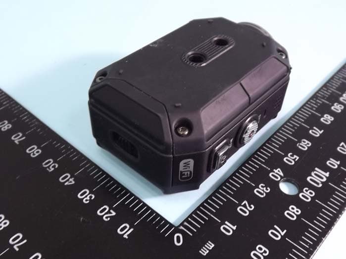
ASIP4C101
Jul 11, 2012Action Camera
Equipment Class
DTS - Digital Transmission System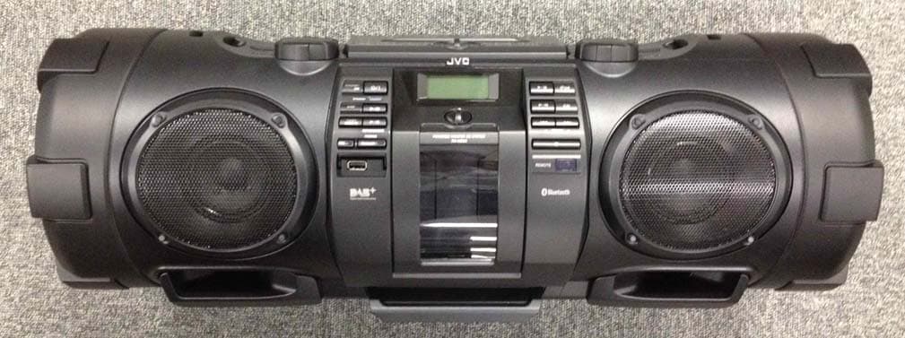
ASIVCB008
Apr 17, 2012POWERED WOOFER CD SYSTEM
Equipment Class
DSS - Part 15 Spread Spectrum Transmitter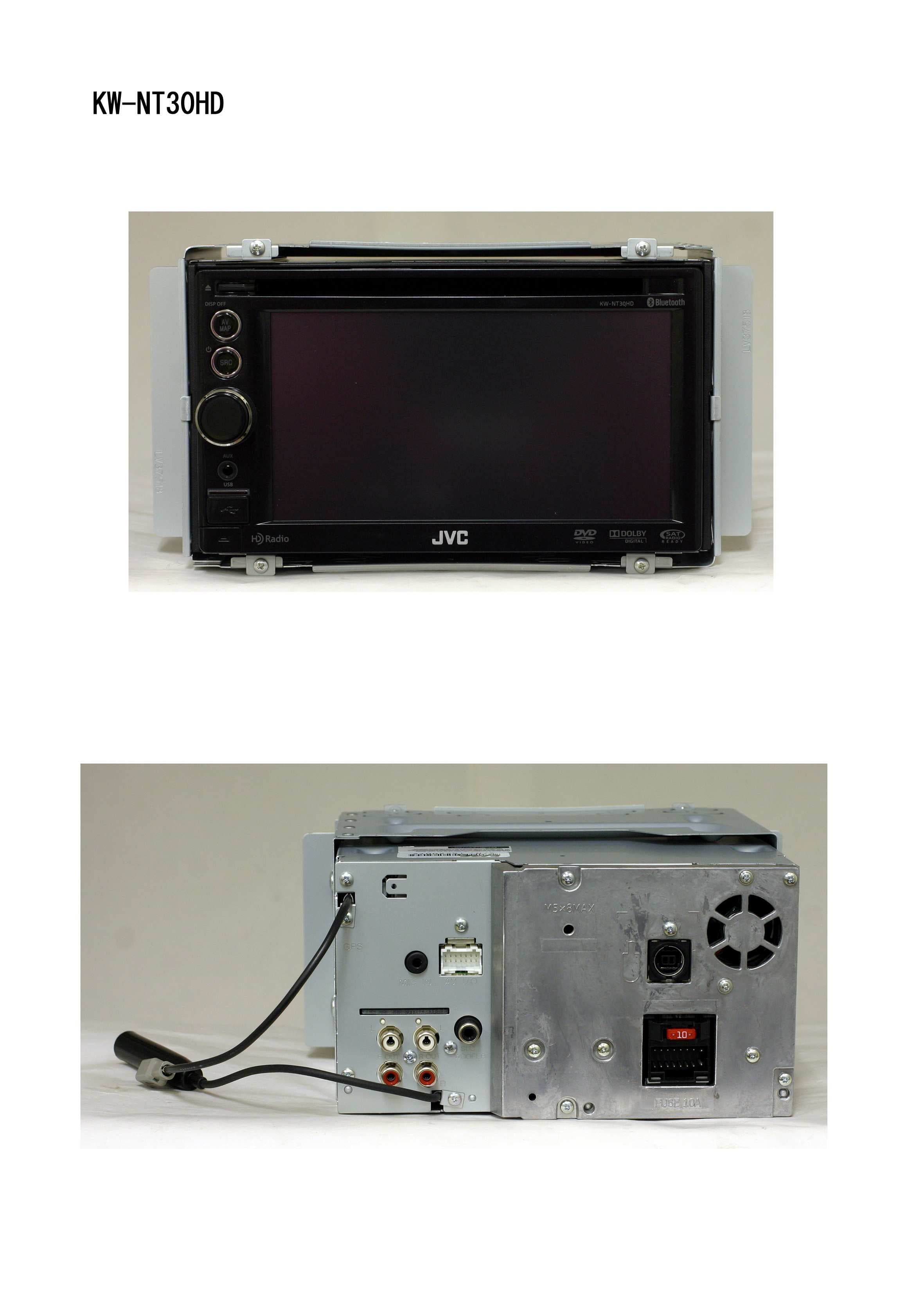
ASIV1B007
Jan 31, 2011GPS Navigation System
Equipment Class
DSS - Part 15 Spread Spectrum Transmitter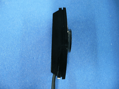
ASIVBA006
Nov 29, 2010Bluetooth audio adaptor for vehicle use.
Equipment Class
DSS - Part 15 Spread Spectrum Transmitter