AZ489FT1625Hand-Held Portable Radio
Motorola Solutions, Inc.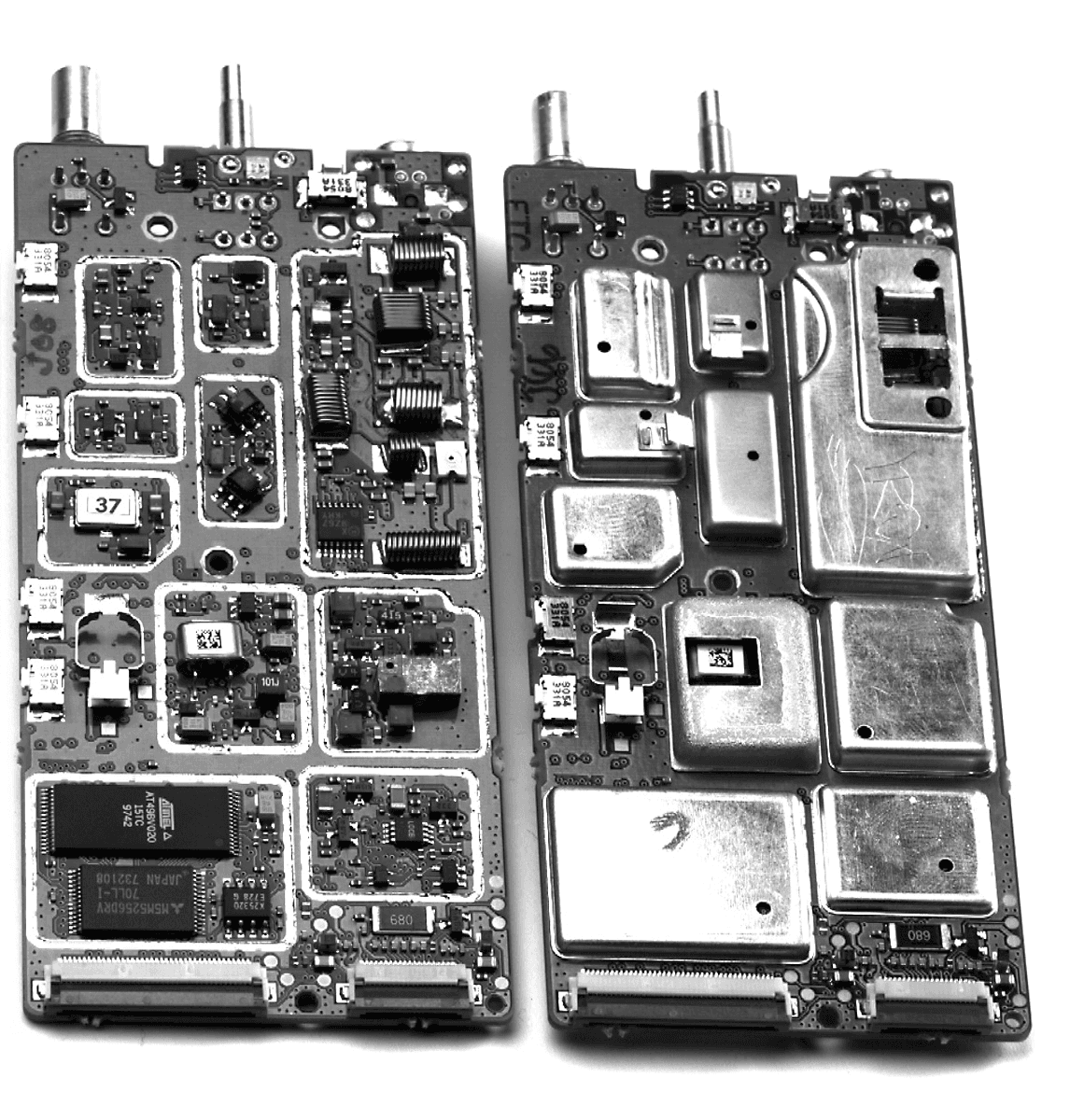
Click to zoom
Application Details
- Equipment Class
- TNF - Licensed Non-Broadcast Transmitter Held to Face
- Date of Grant
- Sep 07, 1998
- Application Purpose
- Original Equipment
- Date of Application
- Jul 05, 1998
- Equipment Note
- Hand-Held Portable Radio
- Frequency Range
- 29.70000000 - 50.00000000
- Company
- Motorola Solutions, Inc.
- Country
- United States
Documents & Files
Document Text
Text extracted from the exhibit documents filed with the FCC. Open a document above to read the original.
Users Manual
GP338 Professional Two-Way Radio Motorola Inc. FCC ID: AZ489FT1625 EXHIBIT 12 English 2-YEAR LIMITED WARRANTY FOR RADIOS We thank you for purchasing our Motorola radios. These radios are manufactured according to the highest quality standards set and are backed by Motorola’s two (2) year warranty. The rechargeable Motorola supplied batteries have a one (1) year warranty. Kindly approach your dealer for more information. Motorola warrants its radios and batteries against defects in material and workmanship under normal use and service for the period stated above. Motorola recommends that you use Motorola supplied accessories and batteries in connection with the radio. We would also advise you against attempting any modifications or repairs or any other form of unauthorised service to your radio. Should you have any queries, please contact: Singapore - Telephone/Fax: (65) 3810408&9/2871068 Beijing- Telephone/Fax: (86-10) 68437222/68438195 Please see next page for more information. Fill in the details of your radio below for your own reference: Model Name/No.: Serial Number: Date of Purchase: Dealer Name: Address: Telephone: #WarisPreUser.book Page 1 27, May 1998, 9:44 AM 4A-1.1Specifications GENERALTRANSMITTER RECEIVER All specifications are subject to change without notice. Low Band Frequency: 29.7---50 MHz Channel Capacity: Popular : 16 Channels Preferred : 128 Channels Power Supply: 7.5 Volts ±20% Dimensions with Standard Capacity NiMH Battery: with High Capacity NiMH Battery: 153mm x 62.3mm x 44mm 153mm x 62.3mm x 46mm Weight: with Standard Capac- ity NiMH Battery: with High Capacity NiMH Battery: 431.3 g 464.8 g Average Battery Life @ (5-5-90 Duty Cycle) Standard Capacity NiMH Battery: High Capacity NiMH Battery: Low Power High Power Sealing: Passes rain testing per IP54 Shock: Meets MIL-STD-810-C,D & E and TIA/EIA 603 Vibration: Meets MIL-STD-810-C,D & E and TIA/EIA 603 Dust: Meets MIL-STD-810-C,D & E and IP54 Humidity: Meets MIL-STD-810-C,D & E and TIA/EIA 603 Low Band RF Output NiMH @ 7.5V: Low 1W High 7 W Frequency: 29.7---50 MHz Channel Spacing: 20/25 kHz Freq. Stability (-30∞C to +60∞C) 0.00025% Spurs/Harmonics: -36 dBm Audio Response: (from 6 dB/oct. Pre- Emphasis, 300 to 3000Hz) +1, -3 dB Audio Distortion: @ 1000 Hz, 60% Rated Max. Dev. <5% FM Noise: -40 dB FCC ID: AZ489FT1625 Low band 25kHz Frequency: 29.7---50 MHz Sensitivity 12dB EIA SINAD: 0.30 mV Adjacent Channel Selectivity ETS -70 dB Intermodulation ETS -65 dB Freq. Stability (-30∞C to +60∞C): 2.5 ppm Spur Rejection: -70 dB Image Rejection: -70 dB Audio Output @ <5% Distortion 500 mW 1 Contents English CONTENTS CONTENTS Radio Overview . . . . . . . . . . . . . . . . . . . . 3 Parts of the Radio. . . . . . . . . . . . . . . . . . . . . . . . 3 On/Off/Volume Knob . . . . . . . . . . . . . . . . . 4Channel Selector Knob. . . . . . . . . . . . . . . . . 4Programmable Buttons . . . . . . . . . . . . . . . . . 4Push-to-Talk (PTT) Button . . . . . . . . . . . . . 7Microphone . . . . . . . . . . . . . . . . . . . . . . . . . 7Menu Keys . . . . . . . . . . . . . . . . . . . . . . . . . . 7Keypad Keys (for keypad radios only) . . . . 8 LCD Screen . . . . . . . . . . . . . . . . . . . . . . . . . . . . 9 Programmable Buttons Audio Indicators . . 11 Getting Started . . . . . . . . . . . . . . . . . . . . 13 Battery Information . . . . . . . . . . . . . . . . . . . . . 13 Battery Status . . . . . . . . . . . . . . . . . . . . . . . 13Charging your Battery . . . . . . . . . . . . . . . . 13 Accessory Information. . . . . . . . . . . . . . . . . . . 14 Attaching the Battery . . . . . . . . . . . . . . . . . 14Removing the Battery . . . . . . . . . . . . . . . . 14Attaching the Antenna . . . . . . . . . . . . . . . . 15Removing the Antenna. . . . . . . . . . . . . . . . 15Attaching the Belt Clip. . . . . . . . . . . . . . . . 15Removing the Belt Clip . . . . . . . . . . . . . . . 16 Turning the Radio On or Off . . . . . . . . . . . . . . 16Adjusting the Radio’s Volume . . . . . . . . . . . . . 16Selecting a Radio Channel . . . . . . . . . . . . . . . . 17Sending a Call. . . . . . . . . . . . . . . . . . . . . . . . . . 17Receiving a Call . . . . . . . . . . . . . . . . . . . . . . . . 17 Radio Calls . . . . . . . . . . . . . . . . . . . . . . . .19 Selective Call . . . . . . . . . . . . . . . . . . . . . . . . . . 19 Making a Selective Call . . . . . . . . . . . . . . . 19Receiving a Selective Call . . . . . . . . . . . . . 19 Call Alert . . . . . . . . . . . . . . . . . . . . . . . . . . . . . 20Radio Check . . . . . . . . . . . . . . . . . . . . . . . . . . . 21Emergency Alarm. . . . . . . . . . . . . . . . . . . . . . . 22Radio Call List . . . . . . . . . . . . . . . . . . . . . . . . . 22 Editing an Entry (for keypad radios only) . 22 Select Zone . . . . . . . . . . . . . . . . . . . . . . . . . . . . 23Talkaround . . . . . . . . . . . . . . . . . . . . . . . . . . . . 23Squelch . . . . . . . . . . . . . . . . . . . . . . . . . . . . . . . 24Power Level . . . . . . . . . . . . . . . . . . . . . . . . . . . 25Tone Tagging . . . . . . . . . . . . . . . . . . . . . . . . . . 25 Name Tone Tagging . . . . . . . . . . . . . . . . . . 25Call Tone Tagging . . . . . . . . . . . . . . . . . . . 26 Scan . . . . . . . . . . . . . . . . . . . . . . . . . . . . .27 Starting or Stopping a Scan Operation . . . . . . . 27 Using the Menu. . . . . . . . . . . . . . . . . . . . . . 27 #WarisPreUser.book Page 1 27, May 1998, 9:44 AM Contents 2 English CONTENTS Using the Scan key . . . . . . . . . . . . . . . . . . . 28 Talkback. . . . . . . . . . . . . . . . . . . . . . . . . . . . . . 28Deleting a Nuisance Channel. . . . . . . . . . . . . . 28Adding a Deleted Nuisance Channel back to the Scan List . . . . . . . . . . . . . . . . . . . . . . . . . . . . . 28Scan Channel Discovery Alert. . . . . . . . . . . . . 28Editing the Scan List . . . . . . . . . . . . . . . . . . . . 29 To Add or Delete Items in the Scan List . . 29 Prioritization of a Scan List …
Text truncated - open the document above for the full version.
Attestation Statements
MOTOROLA INC FCC ID:AZ489FT1625 STATEMENT OF CERTIFICATION The technical data supplied with this application, having been taken under my supervision is hereby duly certified. The following is a statement of my qualifications: 1) MSEE Texas A&M University 1994 2) 4 years experience in the development and testing of Land Mobile Communications Products NAME: Ronald D. Javor SIGNATURE: DATE: 26 May 1998 POSITION: Senior Engineer I hereby certify that the above application was prepared under my direction and that to the best of my knowledge and belief, the facts set forth in the application and accompanying technical data are true and correct: NAME: Philip Craig Warder SIGNATURE: DATE: 26 May 1998 POSITION: Principal Staff Engineer
Attestation Statements
MOTOROLA INC FCC ID:AZ489FT1625 LIST OF EXHIBITS FCC DESCRIPTION EXHIBIT REFERENCE I. Certification of Data12.907 II. Identification label information22.983-(f) III. General Information3 1. Production Plans2.981-(c) 2. Application References2.1061 3. Data Submittal Procedure 4. Similar Applications IV. Description4 1. Technical Characteristics2.983(d)1,2,3,4,5 2. Application V. Function of Semiconductor or52.983-(d)-6 other active devices VI. Circuit Diagrams62.983-(d)-7 VII. Tune-up Procedure72.983-(d)-9 VIII. Circuit Description2.983-(d)-10,11 1. Frequency Stabilizing8A 2. Modulation Limiting8B and Post Limiter Filter 3. Harmonic Suppression8C 4. Power Limiting8D 5. Refer to item 3 & 48E IX. Measured Data2.983-(e) 1.Data Index9 2.RF Output-Data9A2.985 3.Modulation Characteristics2.987 a. Audio Response9B b. Low Pass Filter Response9C c. Modulation Limiting9D 4. Occupied Bandwidth9E2.989 5. Conducted Spurious Emissions 9F2.991 6. Radiated Spurious Emissions9G2.993 7. Frequency Stability (Temp. & Supply Volt)9H2.995 X. Photograph(s)102.983-(g) XI. Instruction Manual112.983-D-8 XII. Measurement Procedure and Test Equip. Used122.999
Cover Letter(s)
FCC ID:AZ489FT3794 ______________________________________________________________________________ Radio Products Group 8000 West Sunrise Boulevard, Fort Lauderdale, Florida 33322. (954) 723-5000 Date: July 01, 1998 Authorization & Evaluation Division Federal Communications Commission Laboratory 7435 Oakland Mills Road Columbia, MD 21046 Subject: Application for Type Acceptance of Transmitter with FCC ID: AZ489FT1625. Attention: George Tannahill, Frank Coperich Gentlemen: Motorola Inc, 8000 West Sunrise Boulevard, Fort Lauderdale, Florida, herein submits application for Type Acceptance of the subject transmitter. This transmitter is primarily intended for use in a portable radio application with capabilities for communications with transmit power of 1 - 7 Watts or 30 dBm to 38.5 dBm. The power is variable 14% of the value listed. The subject transmitter complies with Section 90.203 of the rules in that the operator cannot directly program transmit frequencies using only the unit's normally accessible external controls. Enclosed is a complete Type Acceptance Application. Contact me (954) 723-5793 if you require any additional information. Sincerely, Mike Ramnath FCC Liaison Fax (954) 723-4794
External Photos
MOTOROLA INC FCC ID:AZ489FT1625 PHOTOGRAPHS The following photographs are attached. Front view of plain minus model with antenna Front view of plain minus model without antenna Top of battery Front view of popular keypad model Front view of popular non-keypad model Front view of preferred keypad model Front view of preferred non-keypad model Back of front housing Back of transceiver chassis showing FCC label location Top of radio showing controls Top of keypad board and display Back of keypad board and display Transceiver board and chassis Top of transceiver board without shields Top of transceiver board with shields Back of transceiver board without shields Back of transceiver board with shields EXHIBIT 10 MOTOROLA INC FCC ID:AZ489FT1625 Front view of Plain Minus model with antenna EXHIBIT 10 MOTOROLA INC FCC ID:AZ489FT1625 Front view of Plain MinusFront view of PopularFront view of Popular Model w/o antennaModel w/o antennaKeypad Model w/o antenna MOTOROLA INC FCC ID:AZ489FT1625 Front view of PreferredFront view of Preferred Full Model w/o antennaModel w/o antenna EXHIBIT 10 MOTOROLA INC FCC ID:AZ489FT1625 Back view of radio withView of battery pack battery removed showing showing label and mating FCC label locationcontacts to radio View of radio looking down on controls EXHIBIT 10 MOTOROLA INC FCC ID:AZ489FT1625 Back view of the front housing showing keypad board installed Front view of keypad board Back view of keypad board and display and display EXHIBIT 10 MOTOROLA INC FCC ID:AZ489FT1625 Transceiver Board mounted on chassis EXHIBIT 10 MOTOROLA INC FCC ID:AZ489FT1625 Top side of transceiver board Top side of transceiver board with shields removedwith shields in place EXHIBIT 10 MOTOROLA INC FCC ID:AZ489FT1625 Back side of transceiver board Back side of transceiver board with shields removedwith shields in place EXHIBIT 10
ID Label/Location Info
MOTOROLA INC FCC ID:AZ489FT1625 IDENTIFICATION LABEL LOCATION See The Attached Photograph Or Sketch X Back Of Radio Back Of Radio Under Belt Clip TYPE X The label is a paper polyester film laminate with a pressure sensitive adhesive backing. The adhesive is a permanent type acrylic with a minimum peel strength of 40 oz/inch. MARKINGS (TEXT) X See The Attached Photograph Label Attached Below. See Attached Drawing. EXHIBIT 2
ID Label/Location Info
MOTOROLA INC FCC ID:AZ489FT1625 GENERAL INFORMATION 1. PRODUCTION PLANS: Volume production of this device is planned. 2. APPLICATION REFERENCES: a. Portable Products and their application. b. Portable Products Transmitter Modulation Methods c. Motorola, Boynton Beach Open Area Test Site. 3. DATA SUBMITTAL PROCEDURE: Data is supplied in accordance with Part 2, subpart J of the Commissions’ Rules. 3. SIMILIAR APPLICATIONS: Type Acceptance application with FCC ID:AZ489FT4826. EXHIBIT 3
Operational Description
MOTOROLA INC FCC ID:AZ489FT1625 DESCRIPTION I.Transmitter Technical Characteristics -- Pursuant 2.983 (d) A. RF Power Output1 - 7 Watts (Variable) B. Frequency Range 29.7 - 50 MHz C. Frequency Stability 0.00025 % D. Emissions 16K0F3E E. Spurious Emissions - 51.5dBc F. DC Voltage and Current into 7.5 Volts the final RF amplifier stage/stages 7Amps II.Transmitter Application : This transmitter is primarily intended for use as a hand-held portable radio. The transmitter is characterized by the following features, options and accessories. A. Power Supply Available Attached battery B. Antenna Available 1. Helical X , Telescopic , Whip , Dipole , Dribble External , External _ . C. Squelch Types Available 1. Carrier Squelch X . 2. Tone "Private Line" X . 3. Digital "Private Line" X . D. Microphone - Control 1. Internal Microphone X . 2. Remote Shoulder Mounted Microphone X . E. Maximum Transmit Channel Capability 128 . F. Housing The transmitter will be housed in the housing shown in the accompanying photographs. G. Other Options 1. Single Tone Encoder X 2. Multiple Single Tone Encoder X 3. Touch Code Encoder X 4. Unit ID Encoder X 5. EMS Telemetry Encoder 6. Time out Timer X 7. Voice Encryption X 8. Digital Signaling 9. Sel-Call Decode 10. Trunking X 11. Conventional X 12. Digital Voice EXHIBIT 4
Operational Description
MOTOROLA INC FCC ID:AZ489FT1625 CIRCUIT DESCRIPTION A general description of the overall circuit is covered in the instruction manual. This section provides the description of circuits required by subpart 2.983 of the Commission’s rules. Circuits not described in the manual are covered in this exhibit. The following are included: 1. Means for Frequency Stabilization 8A 2. Means for Limiting Modulation and Low Pass Filtering8B 3. Means for Attenuating Spurious Emissions8C 4. Means for Limiting Power8D 5. Reference Figure for items 3 and 48E EXHIBIT 8 MOTOROLA INC FCC ID:AZ489FT1625 Section 8A - Circuitry for determining and stabilizing frequency This product uses a frequency synthesizer to generate the transmitter signal which is then applied to the transmitter power amplifier. The frequency stability of the output signal from the synthesizer is determined by the stability of the reference frequency applied to the synthesizer input. The figure above shows the frequency synthesizer with the appropriate circuitry highlighted. The reference frequency for the synthesizer is 17.0 MHz. This is determined by the crystal component indicated as Y201 in the figure. Notice also that a varactor, CR211 is connected to one side of the resonator. By varying the voltage applied to the varactor, the frequency of the reference oscillator can be varied. This voltage is supplied from Pin 25 of U205 and is called the warp voltage. The reference oscillator active device is internal to U205 and connects to the resonator at pins 23 and 24. The center frequency of crystal resonators varies in a mathematically predictable way over temperature and following a known polynomial curve. Due to production variations, the coefficients of the curve are slightly different for each crystal. To account for this each crystal is individually characterized and labeled. The integrated circuit U205 contains circuitry which senses the ambient temperature and adjusts the warp voltage to track out the variation in resonator center frequency over temperature. This circuitry is designed to be custom programmed for the slight variations in crystals that are indicated on the crystal label. At the time of production, the label is read and the correct adjustments are programmed into the radio. The reference oscillator is power off a regulated supply voltage. This eliminates variation of the frequency with battery voltage. EXHIBIT 8A MOTOROLA INC FCC ID:AZ489FT1625 Section 8B - Audio Low-pass Filtering and Modulation Limiting Audio processing and modulation limiting are performed inside a custom integrated circuit, U404. This IC takes audio from either the internal or external microphone and performs the necessary processing and outputs modulation information to the synthesizer. The figure below will help explain in the discussion of this operation. ** If the diagram above does not appear, go under the View menu and select Page Layout. Audio from the microphone is routed to a microphone preamp which adjusts for the differences in sensitivity between internal and external microphones. The signal is then routed to a four pole lowpass filter to bandlimit the signal to 4 kHz and then through a highpass filter which remove energy in the low frequency part of the spectrum which is used for signaling. The signal is the preemphasized and then sent to a limiter. This nonlinear circuit clamps the peak value of the audio signal. By limiting this peak value of the audio waveform, we are able to limit the peak value of modulation output to the synthesizer and thereby peak deviation from the transmitter. After the limiter, the audio is passed through a 5 pole lowpass splatter filter to remove higher frequency energy and then subaudible signalling such as CTCSS is summed in. This signal goes through a programmable attenuator before going to the synthesizer. Alignment procedures for the radio will adjust the modulation attenuator and thereby maximum deviation with the audio level driven into limit. The level of the subaudible signaling tone is a known peak value and alignment procedures offset the transmitter deviation setting to insure peak deviation is kept below maximum limit. EXHIBIT 8B Audio From Microphone Modulation output to synthesizer Subaudible Signaling Mic Preamp Mic Lowpass Preemphasis Limiter Splatter Filter Summer Modulation Attenuator Mic Highpass Internal to custom audio processing integrated circuit MOTOROLA INC FCC ID:AZ489FT1625 Section 8C - Attenuation of Spurious Emissions Note: Schematic references refer to the Figure in Section 8E This product is equipped with a lowpass filter following the transmitter output to attenuate spurious harmonics of the transmitter. This filter consists of inductors L100, L101, and L102 as well as capacitors C103, C106, C107, C110, C111, C114 and C116. The elements form a general parameter type lowpass filter with 7 poles and 3 zeros. In addition, the matching of the final device is lowpass in nature. This network is formed by L105,L106 and L107 as well as capacitors C118 - C123 inclusive. Both of these networks attenuate the harmonic emissions from the final amplifier. Section 8D - Limiting of Transmit Output Power Note: Schematic references refer to the Figure in Section 8E This product limits the output power of the transmitter by limiting the dc current into the final device. The current for the RF final amplifier, Q100, flows through resistor R102. The voltage on both sides of this resistor are sensed and connected to a custom integrated circuit which is used for power control functions, U102, at pins 1 and 27. This IC senses the differential voltage across the resistor and compares it to a reference voltage supplied by an internal digital to analog converter. The difference in voltage between these signals controls the magnitude of the output voltage from the IC on Pin 4. Integrated circuit U101 is a RF driver amplifier whose output power is controlled by the magnitude of the voltage applied to pi…
Text truncated - open the document above for the full version.
Parts List/Tune Up Info
MOTOROLA INC FCC ID:AZ489FT1625 Function of RF Semiconductors & Other Active Devices SchematicDeviceCircuit Key Type Application Source D100PIN diodeRF SwitchMACOM D101PIN diodeRF SwitchMotorola Q100MOSFETRF Final AmplifierC-MAC America U101ICRF Driver AmplifierMotorola U102ICRF Power Control ICMotorola VR101ICTemperature SensorNational Semiconductor CR201VaractorOscillator TuningToshiba CR202VaractorOscillator TuningToshiba CR211VaractorOscillator TuningToshiba D201DiodeVoltage MultiplierMotorola Q201BJTBuffer AmplifierHewlett Packard Q202JFETOscillatorPhilips Q203JFETOscillatorPhilips Q204JFETOscillatorPhilips U203VaractorOscillator TuningToshiba U204ICVoltage regulatorAnalog Devices U205ICFrequency Synthesizer ICAtmel U207Dual BJTDC SwitchingRohm CR301VaractorOscillator tuningToshiba Q301BJTOscillatorHewlett Packard U301Dual gate MOSFETIF amplifierPhilips U302ICInverterToshiba U303ICReceiver Backend ICMotorola Q400MOSFETDC switchingPhilips Q403BJTDC switchingMotorola Q405Dual BJTDC switchingRohm Q410Dual BJTDC switchingRohm Q416MOSFETDC switchingPhilips U400ICVoltage RegulatorNational Semiconductor U404ICAudio ProcessingAtmel U407ICEEPROMAtmel U405ICStatic RAMMitsubishi U406ICFlash ROMAtmel U409ICMicroprocessorMotorola U410ICVoltage regulatorImpala Linear U420ICAudio Power AmplifierPhilips CR502Dual BJTLED DriverRohm CR503Dual LEDOperator InterfaceStanley D501Schottky ring quad diodeMixerHewlett Packard D502Dual Schottky diodeAmplitude LimiterMotorola Q509BJTPreampHewlett Packard Q601BJTDC SwitchingMotorola Q602BJTDC SwitchingMotorola Q603BJTDC SwitchingMotorola Q604BJTDC SwitchingMotorola U602ICComparatorMotorola U604Dual BJTDC SwitchingRohm Display ModuleUser InterfaceOptrex EXHIBIT 5 MOTOROLA INC FCC ID:AZ489FT1625 ___________________________________________________________________________________ COMMENTS: The Motorola designators are special code numbers for active devices used in Motorola radios. These devices are either identical or derived from the device family listed under Source, by the manufacturer or are proprietary to Motorola. Service people do not have access to any cross-references or given any information on proprietary devices and are prevented from making unauthorized substitution. EXHIBIT 5
Parts List/Tune Up Info
MOTOROLA INC FCC ID:AZ489FT1625 TUNEUP PROCEDURE Preparations • Place a fully charged battery on the radio or connect the radio to a 7.5 v power supply. • Connect the tuning cable assembly to the radio side connector and to the COM port on the computer used by the tuner program. (Note: This is customizable in the tuner program) • Start the tuner program on the computer. • Power on the radio. • Read the current tuning values by File -> Read Radio Information and SoftPots. Frequency Adjustment • Setup the test equipment to monitor the carrier frequency. • Select frequency adjustment on the tuner with TxAlign -> Reference Oscillator Warp. The tuner will display a screen with single slider control, a PTT Toggle button and a Program button. • Click on the PTT Toggle button to key up the transmitter. • Adjust the slider control with the mouse to warp the transmitter to within 10 Hz. • Click on the PTT Toggle button to dekey the transmitter. • Save the value with the Program button. • Exit the Reference Oscillator Warp function Transmit Power Adjustments Note: The radio supports operation at two different power levels (High and Low) on a channel by channel basis. There are separate alignment screens for high and low power. • Setup the test equipment to measure transmitter power. • Select power adjustment on the tuner with TxAlign -> Transmit Power -> High. The tuner will display a screen with seven slider controls, a PTT Toggle button and a Program button. Each slider corresponds to one RF frequency subrange. • Select the first slider. • Click on the PTT Toggle button to key up the transmitter. • Adjust the slider control with the mouse to set the transmitter power to the value as indicated in the table below: Radio Power Power Set Point 6 watts6.6 watts 5 watts5.5 watts 4 watts4.4 watts 3 watts3.3 watts 2 watts2.2 watts 1 watt1.1 watts • Click on the PTT Toggle button to dekey the transmitter. • Repeat for each subrange. • Save the values with the Program button. • Exit the Transmit Power function. • If the radio is uses only high power channels, proceed to adjust deviation. If low power channels are used, repeat the procedure above for low power alignment by selecting TxAlign - > Transmit Power -> Low. EXHIBIT 7 MOTOROLA INC FCC ID:AZ489FT1625 TUNEUP PROCEDURE (Continued) Transmit Deviation • Setup the test equipment to measure deviation. • Inject a 1000 mV peak to peak tone at 1000 Hz into the tuning cable assembly Audio In port. • Select deviation adjustment on the tuner with TxAlign -> VCO Attenuation. The tuner will display a screen with seven slider controls and a PTT Toggle button. Each slider corresponds to one RF frequency subrange. • Select the first slider. • Click on the PTT Toggle button to key up the transmitter. • Adjust the slider control with the mouse to set the transmitter deviation to as indicated in the table below: Channel Spacing Deviation Setting 20.0 kHz4.50 kHz • Click on the PTT Toggle button to dekey the transmitter. • Repeat for each subrange. • Save the values with the Program button. • Exit the VCO Attenuation function. Modulation Balance • Setup the test equipment to measure deviation. • Inject a 100 mV peak to peak tone at 80 Hz into the tuning cable assembly Audio In port. • Select modulation balance adjustment on the tuner with TxAlign -> Modulation Balance Attn. The tuner will display a screen with seven slider controls, a PTT Toggle button and a Program button. Each slider corresponds to one RF frequency subrange. • Select the first slider. • Click on the PTT Toggle button to key up the transmitter. • Note the deviation from the 80 Hz tone. • Change the tone frequency to 3000 Hz. • Adjust the slider control with the mouse to set the transmitter deviation to with 2% of the value at 80 Hz. • Click on the PTT Toggle button to dekey the transmitter. • Repeat for each subrange. • Save the values with the Program button. • Exit the Modulation Balance Attn. function. EXHIBIT 7
Schematics
MOTOROLA INC FCC ID:AZ489FT1625 SCHEMATIC DIAGRAMS The following schematic diagrams will be similar to those that appear in the final service manual. 1) Frequency Generation Unit. a) Frequency Generation Unit b) Synthesizer c) Voltage Controlled Oscillator 2) Transmitter. The sheets are incorporated found in an associated Adobe PDF file included with this application. The name of the Adobe PDF file is AZ489FT1625_Exhibit 6.pdf EXHIBIT 6
Schematics
11 .01uF C145 220nH .01uF L109 5V_TX CSX CLK DATA RESET BATT_B+_4 C111 SEE TABLE SEE TABLE SEE TABLE SEE TABLE SEE TABLESEE TABLE .01uF C126 .01uF C124 .01uF C146 SEE TABLE C110 R110 24K C139 .01uF L110 L103 750nH C123 510pF 1000pF C130 V5EXT 17 VAR1 20 VAR2 18 VAR3 24 VG 15 VL 6 VLIM 19 RFIN 1 RS 21 RSET 31 RX 23 T1 2 TEMP 30 14 V10V45 16 DATA 28 9 F168 GND1 8 GND2 25 INT 4 NA 22 Q 11 QX 10 BPOS 27 CEX 29 3 CI CJ 5 CL 7 CLK 26 CQ 12 CQX 13 U102 H99S-4 ANO 32 100 R112 470K R114 .01uF C142 IF108 IF104 1000pF R103 200 C141 C140 1000pF SWITCH S100 12 E100 BEAD C135 SEE TABLE C115 SEE TABLE L107 6.2K R104 R108 10 510pF R111 12K C122 C134 .01uF C127 10uF C143 .01uF 1 2 3 5 4 100 T100 XFMR R113 2 3 R115 10 RF_JACK J101 GND 4 1 NC4 15 RFIN 166 RFOUT1 RFOUT2 7 VCNTRL 1 VD1 14 VG1 2 VG2 3 G2 11 4 GND1 5 GND2 12 GND3 13 GND4 NC1 8 NC2 9 NC3 10 09Z67 U101 0.1uF C125 C114 SEE TABLE C131 1000pF 200 R101 C147 22pF C107 SEE TABLE IF109 470 C138 R107 .01uF 0.1uF C133 C132 .01uF R102 0.1 SEE TABLE C106 C136 .01uF R106 200 D100 C144 .01uF 4 TAB4 Q100 ANTENNA_NUT J102 1 TAB1 2 TAB2 3 TAB3 L104 2.2uH C103 SEE TABLE D101 C121 180pF R109 1K L101 L102 L100 L106 IF103 47pF C118 200 R105 180pF C120 0.1uF SHIELD SH100 C128 R117 1MEG 2K 3 GND 1 POS VOUT 2 R116 IF101 LM50 VR101 IF107 IF105 L105 IF106 L108 220nH C129 .01uF 1000pF C119 47pF C137 IF102 C108 1uF RX_IN AUX4 EMER TX_INJ FL0830035P Low Band RF Board Transmitter Schematic Circuit Reference Range 1 29.7 — 42 MHz Range 2 35 — 50 MHz Motorola Part Number Description Motorola Part Number Description CAPACITOR, Fixed: pF ± 5%; 50V unless stated CAPACITOR, Fixed: pF ± 5%; 50V unless stated C1032113740F38302113740F3318 C1062113740F44512113740F4139 C1072113740F47682113740F4556 C1102113740F42432113740F4036 C111, C114 2113740F48752113740F4556 C1152113740F33182113740F3115 INDUCTOR, RF:INDUCTOR, RF: L100 2460591X13125nH2460591X12110nH L1012460591X08166nH2460591X14137nH L1022460591X12110nH2460591X1689nH L1052460591X09110nH2460591X13125nH L1062460591X1050nH2460591X1546nH L1072409348J055.6nH2409348J043.6nH Circuit Reference Range 1 29.7 — 42 MHz Range 2 35 — 50 MHz Motorola Part Number Description Motorola Part Number Description 15 IF235 VCO SYNTH AUX2AUX3PRE_IN RX_INJ TX_INJ VCTRLVSF IF204 IF258IF234IF240IF229IF231 IF200 IF233IF232 IF208 IF241 IF201IF207 IF237IF239 IF206IF202 IF242IF243 IF205IF203 AUX2 AUX3AUX4 CLK CSXDATALOCKMODIN PRE_IN SWB+ VCTRL VDD VSF 5V_RXCLK_TXCLK_RXDATA_RX DATA TX_INJ16_8_MHZ_RX 16_8_MHZ SWB+_RX SWB+ VDD_RXDATA_TXRX_INJ LOCK MODIN CLK CSX_TX5V_TX 5V AUX4 CSX VDD 16.8MHZ 5V FL0830039P Low Band RF Board FGU Leaded Part 1 Schematic 16 IF264 2 IF272 CR501 1 IF210 IF259 IF216 IF276IF277 12 PB503 SWITCH M200 IF275 IF260 IF263 IF217 IF267 IF278 IF209 IF212 IF228IF218 IF273 IF224 IF271IF274 M201 2 1 IF225IF211 F1 24V 3A C503 IF261 100pF IF268 IF279 IF223 IF280 IF222 IF265 IF221 1 2 IF220 IF266 IF226 SWITCH PB502 IF230 IF214IF227 IF270 IF213 RTA3_2 UNSWB+_1 BATT_B+_2 UNSWB+_2 MECH_SW_B+_2 SB3SB2 LI_ION IF215 DEMOD_1 SQ_OUT_1 DEMOD_2SQ_OUT_2 BATT_CODE_1 BATT_CODE_2 EMER_1 EMER_3 RSSI_1 RSSI_2 RESET_1 RESET_3 VOL_1 VOL_2 RED_LED_1 GREEN_LED_1 RED_LED_2GREEN_LED_2 PTT_1 PTT_2 LVZIF_SEL_1 LVZIF_SEL_2 SB1_1 SB1_2 MECH_SW_B+_1 RTA0_1RTA1_1 RTA0_2RTA1_2 RTA2_1RTA3_1 RTA2_2 FL0830040P Low Band RF Board FGU Leaded Part 2 Schematic 17 CR211 2.2uH L222 1 C298.01uF 13 VRO WARP 25 XTAL1 23 XTAL2 24 SH200 SHIELD TEST1 37 TEST2 38 VBPASS 21 VCP 47 VMULT1 15 VMULT2 14 VMULT3 12 VMULT4 11 PRE_GND 33 PRE_VDD 34 PVREF 35 REFSEL 18 SFBASE 27 SFCAP 26 SFIN 30 SFOUT 28 LOCK MODIN 10 MODOUT 41 NC1 17 NC2 29 NC3 31 PD_GND 44 5 PD_VDD PREIN 32 DATA 7 DGND 6 DVDD 36 FREFOUT 19 IADAPT 45 INDMULT 16 IOUT 434 AUX3 2 AUX4 3 AVDD 20 BIAS1 40 BIAS2 39 CCOMP 42 CEX 9 CLK 8 U205 63A27 ADAPTSW 46 AGND 22 AUX1 48 AUX2 1 L223100uH 2.7pFC237 2.2uF 2K R229 C258 1 OUT 2 OUT 0 R221 17.0MHz 75Z02 Y201 GND 3 OUT IN C259 1uF 100uH L225 C248 0.1uF .01uF .01uF C264 430 C260 R224 C2474.7uF R223100K R228 51 0.1uF 1 TP201 TEST_POINT 1 C265 R230 TEST_POINT TP200 .047uF 0 C257 C249 .01uF 0.47uFC234 C238 0.1uF D201 C24247pF R222 75K SHIELD SH201 1 R225 750 4 OUT 3 SD U204 ADP3300 6 ERR 1 GND 5 IN 2…
Text truncated - open the document above for the full version.
Contact Information
Applicant
Deanna Zakharia(Regulatory Compliance Manager)
Technical Contact
Motorola IncMike Ramnath
[email protected](954) 723-5793
8000 West Sunrise Boulevard · Fort Lauderdale, Florida · United States
Non-Technical Contact
Motorola IncMike Ramnath
[email protected](954) 723-5793
Technical Specifications
| # | Rule Parts | Frequency Range | Power Output | Emission | Tolerance |
|---|---|---|---|---|---|
| 1 | 90 | 29.7 MHz - 50 MHz | 7 W | 16K0F3E | 2.5000000000 ppm |
Other Applications from Motorola Solutions, Inc.
AZ489FT4980
Sep 08, 2026Portable two way radio
Equipment Class
TNF - Licensed Non-Broadcast Transmitter Held to FaceAZ489FT4981
Aug 14, 2026Handheld Portable - TANAPA BPR 45 400-470 MHZ 4W NKP
Equipment Class
TNF - Licensed Non-Broadcast Transmitter Held to Face
AZ489FT7187
Jul 13, 2026Portable 2-Way Radio with Bluetooth, Bluetooth LE, WIFI 2.4GHz, WIFI 5GHz, LTE
Equipment Class
DSS - Part 15 Spread Spectrum TransmitterAZ499FT6031
May 11, 2026Operation Critical Wireless Earpiece PTT
Equipment Class
DSS - Part 15 Spread Spectrum Transmitter
AZ499FT5879
Dec 19, 20252-way Portable Radio with BT, BTLE, WIFI, NFC and LTE
Equipment Class
DSS - Part 15 Spread Spectrum Transmitter