AZ489FT3799Hand Held Transmitter
Motorola Solutions, Inc.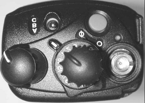
Click to zoom
Application Details
- Equipment Class
- TNF - Licensed Non-Broadcast Transmitter Held to Face
- Date of Grant
- Mar 27, 2000
- Application Purpose
- Original Equipment
- Date of Application
- Feb 29, 2000
- Equipment Note
- Hand Held Transmitter
- Frequency Range
- 136.00000000 - 174.00000000
- Company
- Motorola Solutions, Inc.
- Country
- United States
Documents & Files
Document Text
Text extracted from the exhibit documents filed with the FCC. Open a document above to read the original.
Users Manual
MOTOROLA INC.FCC ID: AZ489FT3799 EXHIBIT 8 INSTRUCTION MANUAL x Preliminary Manual Attached. Complete Manual Attached. Note: See XTS3500bsm.pdf document to view XTS3500 Basic Service Manual information.
Users Manual
1 ™ Digital XTS 3500 ™ Portable Radios Basic Service Manual 2 Foreword This manual covers all models of the ASTRO™ Digital XTS 3500 ® Portable Radio, unless otherwise specified. It includes all the information necessary to maintain peak product performance and maximum working time, using the pass/fail service approach. This basic level of service is typical of some local service centers, self-maintained customers, and some distributors. Included in this manual are: radio specifications for the VHF and UHF frequency bands; a general description of ASTRO Digital XTS 3500 models; recommended test equipment, service aids, and tools; radio alignment procedures; fundamental disassembly/reassembly procedures; and general maintenance recommendations. For details on the operation of the radio, or board or component-level troubleshooting, refer to the applicable manuals, available separately. To help you with your selection, a list is provided under “Related Publications” at the front of this manual. Safety Before operating an ASTRO XTS 3500 Radio, please read the “Safety Information” section in the front of this manual. Manual Revisions Changes which occur after this manual is printed are described in “FMRs.” These FMRs provide complete information on changes, including pertinent parts list data. i Table of Contents Foreword . . . . . . . . . . . . . . . . . . . . . . . . . . . . . . . . . . . . . . . . . . . . . . . . . . . . . . . . . . inside front cover List Of Figures. . . . . . . . . . . . . . . . . . . . . . . . . . . . . . . . . . . . . . . . . . . . . . . . . . . . . . . . . . . . ii List of Tables. . . . . . . . . . . . . . . . . . . . . . . . . . . . . . . . . . . . . . . . . . . . . . . . . . . . . . . . . . . . . ii Related Publications . . . . . . . . . . . . . . . . . . . . . . . . . . . . . . . . . . . . . . . . . . . . . . . . . . . . . . iii Portable Radio Model Numbering System. . . . . . . . . . . . . . . . . . . . . . . . . . . . . . . . . . . . . iv Specifications for VHF Radios. . . . . . . . . . . . . . . . . . . . . . . . . . . . . . . . . . . . . . . . . . . . . . . . v Specifications for UHF Radios. . . . . . . . . . . . . . . . . . . . . . . . . . . . . . . . . . . . . . . . . . . . . . . vi Glossary . . . . . . . . . . . . . . . . . . . . . . . . . . . . . . . . . . . . . . . . . . . . . . . . . . . . . . . . . . . . . . . . vii Safety Information . . . . . . . . . . . . . . . . . . . . . . . . . . . . . . . . . . . . . . . . . . . . . . . . . . . . . . . . x 1 - Introduction . . . . . . . . . . . . . . . . . . . . . . . . . . . . . . . . . . . . . . . . . . . . . . . . . . . . . . . . . . . 1 General . . . . . . . . . . . . . . . . . . . . . . . . . . . . . . . . . . . . . . . . . . . . . . . . . . . . . . . . . . . . . . . . . . . . . . . 1 Notations Used in This Manual . . . . . . . . . . . . . . . . . . . . . . . . . . . . . . . . . . . . . . . . . . . . . . . . . . . . 1 Radio Description . . . . . . . . . . . . . . . . . . . . . . . . . . . . . . . . . . . . . . . . . . . . . . . . . . . . . . . . . . . . . . . 2 FLASHport . . . . . . . . . . . . . . . . . . . . . . . . . . . . . . . . . . . . . . . . . . . . . . . . . . . . . . . . . . . . . . . . . . . . . 2 2 - Basic Maintenance . . . . . . . . . . . . . . . . . . . . . . . . . . . . . . . . . . . . . . . . . . . . . . . . . . . . . .3 Introduction to This Section . . . . . . . . . . . . . . . . . . . . . . . . . . . . . . . . . . . . . . . . . . . . . . . . . . . . . . 3 Preventive Maintenance . . . . . . . . . . . . . . . . . . . . . . . . . . . . . . . . . . . . . . . . . . . . . . . . . . . . . . . . . . 3 Handling Precautions . . . . . . . . . . . . . . . . . . . . . . . . . . . . . . . . . . . . . . . . . . . . . . . . . . . . . . . . . . . . 4 3 - Recommended Test Equipment and Service Aids . . . . . . . . . . . . . . . . . . . . . . . . . . . . . 5 Recommended Test Equipment . . . . . . . . . . . . . . . . . . . . . . . . . . . . . . . . . . . . . . . . . . . . . . . . . . . . 5 Service Aids . . . . . . . . . . . . . . . . . . . . . . . . . . . . . . . . . . . . . . . . . . . . . . . . . . . . . . . . . . . . . . . . . . . . 5 Field Programming Equipment . . . . . . . . . . . . . . . . . . . . . . . . . . . . . . . . . . . . . . . . . . . . . . . . . . . . 6 4 - Performance Checks . . . . . . . . . . . . . . . . . . . . . . . . . . . . . . . . . . . . . . . . . . . . . . . . . . . . .7 Introduction to This Section . . . . . . . . . . . . . . . . . . . . . . . . . . . . . . . . . . . . . . . . . . . . . . . . . . . . . . 7 Setup . . . . . . . . . . . . . . . . . . . . . . . . . . . . . . . . . . . . . . . . . . . . . . . . . . . . . . . . . . . . . . . . . . . . . . . . . 7 Display Radio Test Mode . . . . . . . . . . . . . . . . . . . . . . . . . . . . . . . . . . . . . . . . . . . . . . . . . . . . . . . . . 7 Non-Display Radio Test Mode . . . . . . . . . . . . . . . . . . . . . . . . . . . . . . . . . . . . . . . . . . . . . . . . . . . . 10 5 - Radio Alignment Procedures . . . . . . . . . . . . . . . . . . . . . . . . . . . . . . . . . . . . . . . . . . . . . 15 Introduction to This Section . . . . . . . . . . . . . . . . . . . . . . . . . . . . . . . . . . . . . . . . . . . . . . . . . . . . . 15 General . . . . . . . . . . . . . . . . . . . . . . . . . . . . . . . . . . . . . . . . . . . . . . . . . . . . . . . . . . . . . . . . . . . . . . 15 Reference Oscillator Alignment . . . . . . . . . . . . . . . . . . . . . . . . . . . . . . . . . . . . . . . . . . . . . . . . . . . 17 Transmit Power Alignment. . . . . . . . . . . . . . . . . . . . . . . . . . . . . . . . . . . . . . . . . . . . . . . . . . . . . . . 18 Transmit Deviation Balance (Compensation) Alignment . . . . . . . . . . . . . . . . . . . . . . . . . . . . . . . 19 Transmit Deviation Limit Alignment. . . . . . . . . . . . . . . . . . . . . . . . . . . . . . . . . . . . . . . . . . . . . . . 20 Front End Filter Alignment. . . . . . . . .…
Text truncated - open the document above for the full version.
Attestation Statements
MOTOROLA INC FCC ID: AZ489FT3799 EXHIBIT 2 STATEMENT OF CERTIFICATION The technical data supplied with this application, having been taken under my supervision is hereby duly certified. The following is a statement of my qualifications: 1) MSEEOklahoma State University MBA Oklahoma State University 2) 6 years experience in the development, testing and certification of Land Mobile Communications Products NAME: Stephen L. Kersten SIGNATURE: DATE: 21 February 2000 POSITION: Senior Staff Electrical Engineer I hereby certify that the above application was prepared under my direction and that to the best of my knowledge and belief, the facts set forth in the application and accompanying technical data are true and correct: NAME: Daniel Marks SIGNATURE: DATE: 21 February 2000 POSITION: Engineering Manager
Attestation Statements
MOTOROLA INC FCC ID: AZ489FT3799 RF EXPOSURE INFORMATION: In accordance with 47 CFR 2.1093 (c), this transmitter has been subjected to routine environmental evaluation for RF exposure and found to be compliant with the limits specified in 47 CFR 2.1093 (d). EXHIBIT 11
Block Diagram
MOTOROLA INC.FCC ID: AZ489FT3799 BLOCK DIAGRAMS & CIRCUIT DESCRIPTION A general description of the overall circuit is covered in the instruction manual. This section provides the description of circuits required by subpart 2.983 of the Commissions’ rules. Circuits not described in the manual are covered in this exhibit. The following are included: 1.Means for Carrier Frequency Generation and Stabilization4A 2.Means for Modulation Limiting and Low Pass Filter4B 3.Means for Harmonic Suppression4C 4.Means for Power Limiting4D EXHIBIT 4 MOTOROLA INC.FCC ID: AZ489FT3799 CARRIER FREQUENCY GENERATION AND STABILIZATION Circuit Description: The carrier frequency is generated using a fractional-N frequency synthesizer. This consists of a phase-locked loop circuit with a voltage controlled oscillator (VCO) whose output is fed back to a programmable divider chain. The divide ratios are determined from information stored in the memory ICs and bussed to the synthesizer via a microcomputer. The microcomputer extracts the data for the division ratios as determined by the system select switch or by loading data stored in the memory ICs. Using a time averaged algorithm a combination of divide ratios are used so that the reference frequency can be a much higher value than the value of the frequency resolution. Modulation occurs by a combination of directly coupling the modulation signal to the low pass filter in the loop and by processing the digitized analog modulation signal to alter the divider values. A temperature compensated crystal oscillator, operating at 16.8 MHz and stable to 2.0 parts per million over temperature extremes is used for the frequency reference. The 16.8 MHz reference is further divided into one of three reference frequencies which is compared to the divided down VCO output in a phase detector which in turn provides a DC steering voltage back to the VCO. A Block diagram of the VCO/Synthesizer system is shown below. EXHIBIT 4A MOTOROLA INC.FCC ID: AZ489FT3799 MODULATION LIMITING AND LOW PASS FILTERING Circuit Description: The pre-emphasis, modulation limiting and low pass filtering of this transmitter are accomplished in the Digital Signal Processor IC (U602) using software implementations of digital filters. Analog audio is digitized in the DSP Support IC (U603) and then transferred to the DSP (U602) where it is pre-emphasized and scaled. Sub-audible tones and audio frequency signaling information is generated in the DSP, scaled, and summed with audio. The combined signal is then filtered using a low pass filter. Signals are then returned to the DSP Support IC (U603) and converted to analog signals. The limited, filtered audio is then fed through digitally programmable attenuators to the modulation ports on the synthesizer module. Digital mode modulation is similar, except no pre- emphasis or summing is required. A block diagram of the limiting and low pass filtering is shown below. EXHIBIT 4B MOTOROLA INC.FCC ID: AZ489FT3799 HARMONIC SUPPRESSION CIRCUIT Circuit Description: Additional attenuation for harmonics is provided by a low pass filter between the Antenna Switch and the Antenna port. The VHF transceiver uses a seventh order, three pole, elliptic low pass filter as shown in the diagram below. The input is on the left, from the antenna switch, at C105. The output is on the right, to the antenna connector. Circuit Diagram: EXHIBIT 4C MOTOROLA INC.FCC ID: AZ489FT3799 POWER LIMITING The transmitter automatic level control (ALC) circuit consists of the following functional blocks. AR1Power Amplifier (PA) DC1Directional coupler D1RF detector U1Power Control IC (PCIC) DC1 AR1 D1 To Antenna Switch Modulated RF from Synthesizer C1 R1 U1 D/A #1 Figure 1 - Transmitter ALC Block Diagram Power amplifier (PA) AR1 amplifies the modulated radio frequency (RF) signal to the rated output power level of the radio. The PA gain is adjustable by means of a control voltage signal (Vctrl) from the Power Control IC (PCIC). Increasing Vctrl increases the PA gain. Directional coupler DC1 couples a fixed fraction of the PA forward power into detector D1. The output of detector D1 is a DC voltage (Vdet) with an amplitude proportional to the PA forward power. At the PCIC (U1) signal Vdet connects to the inverting input of an operational amplifier. Internal D/A converter (D/A#1) is programmed to a reference voltage (Vref) which is proportional to the output power set point. Constants of proportionality are computed by the factory tuning procedure for each radio over the range of powers and frequencies, and stored in the radio’s internal non-volatile memory. Vref connects to the non-inverting input of the op-amp. The ALC loop is levelled when Vdet is equal to Vref. PCIC maintains Vctrl at the voltage required to level the loop. Loop transient response is determined by time constants which are set by the PCIC internal programmable resistor R1 and external capacitor C1. MOTOROLA INC.FCC ID: AZ489FT3799 EXHIBIT 4D Thus the transmitter ALC maintains a constant power level over all radio operating conditions. Accuracy is determined by the linearity of DC1 and D1, and the settabillity of D/A#1. EXHIBIT 4E
Cover Letter(s)
FCC ID:AZ489FT4828 ______________________________________________________________________________ Radio Products Group 8000 West Sunrise Boulevard, Fort Lauderdale, Florida 33322. (954) 723-5000 Date:February 29, 2000 Authorization & Evaluation Division Federal Communications Commission Laboratory 7435 Oakland Mills Road Columbia, MD 21046 Subject: Application for Certification of Transmitter with FCC ID: AZ489FT3799. Attention: Frank Coperich, George Tannahill. Gentlemen: Motorola Inc, 8000 West Sunrise Boulevard, Fort Lauderdale, Florida, herein submits application for Certification of the subject transmitter. This transmitter is intended for use in a Portable Radio environment with capabilities for clear and coded communications with a variable transmit power of 1-6 Watt (30-37.8 dBm). The subject transmitter complies with Section 9.203 of the Rules in that the operator cannot directly program transmit frequencies using the unit's normally accessible external controls. A complete Certification application is enclosed, contact Mike Ramnath at (954)723-5793 or Fax (954)723-4794 if you require any additional information. Sincerely, Mike Ramnath FCC Liaison Email: [email protected] EXHIBIT 13
External Photos
MOTOROLA INC.FCC ID: AZ489FT3799 EXTERNAL PHOTOGRAPHS The following photographs are attached. 1.Front view. 2.Back view with battery. 3.Back view (FCC label location). 4.Side view (Right). 5.Side view (Left). 6.Top view (Controls). EXHIBIT 3 MOTOROLA INC.FCC ID: AZ489FT3799 FRONT VIEW EXHIBIT 3-1 MOTOROLA INC.FCC ID: AZ489FT3799 BACK VIEW WITH BATTERY EXHIBIT 3-2 MOTOROLA INC.FCC ID: AZ489FT3799 BACK VIEW (FCC LABEL) EXHIBIT 3-3 MOTOROLA INC.FCC ID: AZ489FT3799 SIDE VIEW (RIGHT) EXHIBIT 3-4 MOTOROLA INC.FCC ID: AZ489FT3799 SIDE VIEW (LEFT) EXHIBIT 3-5 MOTOROLA INC.FCC ID: AZ489FT3799 TOP VIEW EXHIBIT 3-6
ID Label/Location Info
MOTOROLA INC FCC ID: AZ489FT3799 IDENTIFICATION LABEL LOCATION See the attached Photograph or Sketch X Back of Radio Back of Radio under Belt Clip TYPE X The label is a paper polyester film laminate with a pressure sensitive adhesive backing. The adhesive is a permanent type acrylic with a minimum peel strength of 40 oz/inch. MARKINGS (TEXT) X See the Attached Photograph Label Attached Below. See Attached Drawing. EXHIBIT 1 MOTOROLA INC FCC ID: AZ489FT3799 GENERAL INFORMATION I.Production Plans -- Pursuant 2.981 (c) Quantity production is planned. II.Application References -- Pursuant 2.1061 Reference is made to the following Motorola "Application References" 1. Portable Products and their application. 2. Portable Products Transmitter Modulations Methods. 3. Plantation, Florida Antenna Range. III.Data Submittal Procedure: Data is supplied in accordance with Part 2, Sub-part J of the Commissions’ rules. Necessary Bandwidth Computation for 8K10F1E Emission Designator The FCC Rule & Regulations Part 2, §2.202(b) defines Necessary Bandwidth as the minimum value of the occupied bandwidth sufficient to ensure that transmission of information at the rate and with the quality required for the system employed. §2.202(c) lists four methods of determining the necessary bandwidth, including the use of formulas in §2.202(g), and measurement in cases where the other methods of §2.202(c) do not apply. It is felt that while these formulas apply well to voice and many older digital modulation systems, the formulas do not apply to the high performance digital modulation employed in the system submitted for type acceptance because of difficulties determining representative values for the factors K and M. We have, therefore, used the measurement criteria of §2.202(c)(4). The value cited, 8K10, is the bandwidth that contains 99% of the total transmitted power. The 99% value was chosen because §2.202(b) defines Necessary Bandwidth as the minimum value of the occupied bandwidth. In turn, §2.202(b) defines Occupied Bandwidth as the frequency bandwidth such that, below its lower and above its upper frequency limits, the mean powers radiated are each equal to 0.5% of the total mean power radiated by a given emission, i.e., contains 99% of the total transmitted power. IV.Applicable References: ∑ Reference Type Acceptance FCC ID: AZ489FT4821 ∑ EIA/TIA-603 Land Mobile FM or PM Communications Equipment Measurement and Performance Standards ∑ FCC Federal Regulations Part 47 Sec. 2.983-2.999 ∑ FCC Federal Regulations Part 90 Sec.90.210 EXHIBIT 1a
Internal Photos
MOTOROLA INC.FCC ID: AZ489FT3799 INTERNAL PHOTOGRAPHS The following photographs are attached. 1.RF board (Top). 2.RF board (Bottom). 3.Vocon board (Top). 4.Vocon board (Bottom). EXHIBIT 9 MOTOROLA INC.FCC ID: AZ489FT3799 RF BOARD (TOP VIEW) EXHIBIT 9-1 MOTOROLA INC.FCC ID: AZ489FT3799 RF BOARD (BOTTOM VIEW) EXHIBIT 9-2 MOTOROLA INC.FCC ID: AZ489FT3799 VOCON BOARD (TOP VIEW) EXHIBIT 9-3 MOTOROLA INC.FCC ID: AZ489FT3799 VOCON BOARD (BOTTOM VIEW) EXHIBIT 9-4
Operational Description
MOTOROLA INC FCC ID: AZ489FT4828 DESCRIPTION I.Transmitter Technical Characteristics -- Pursuant 2.983 (d) A. RF Power Output1 - 6 Watt (Variable) B. Frequency Range136 - 174 MHz C. Frequency Stability0.00020 % D. Emissions16K0F3E,11K0F3E, 8K10F1E, 8K10F1D, 20K0F1E E. Spurious Emissions- 75 dBc F. DC Voltage and Current into7.5 Volts the final RF amplifier stage/stages 2.0Amps II.Transmitter Application : This transmitter is primarily intended for use as a hand-held portable radio. The transmitter is characterized by the following features, options and accessories. A. Power Supply Available Ni-Cad Battery X , Mercury Battery , , Alkaline Battery , AC , Lead Acid Battery , Ni-MH Battery X ,Li-Ion X B.Antenna Available 1. Helical X , Telescopic , Whip X , Dipole , Dribble External , External . C. Squelch Types Available 1. Carrier Squelch X . 2. Tone "Private Line" X . 3. Digital "Private Line" X . D. Microphone - Control 1. Handset/Palm Microphone X 2. Wireline control X . E. Maximum Transmit Channel Capability 250 . F. Housing The transmitter will be housed in the housing shown in the accompanying photographs. G. Other Options 1. Single Tone Encoder X 2. Multiple Single Tone Encoder 3. Touch Code Encoder 4. Unit ID Encoder X 5. EMS Telemetry Encoder 6. Time out Timer X 7. Voice Encryption X 8. Digital Signaling X 9. Sel-Call Decode X 10. Trunking X 11. Conventional X 12. Digital Voice X _ EXHIBIT 12
Parts List/Tune Up Info
MOTOROLA INC.FCC ID: AZ489FT3799 Function of RF Semiconductors & Other Active Devices Schematic DesignatorDeviceCircuit KeyMotorolaTypeApplicationSource U1057W50ICRF AmpMotorola U3057W52ICMixerMotorola Q4018N55ICIF AmpPhilips Y20163A22ModuleRef. OscillatorMotorola U20363A27ICSynthesizerMotorola U20250U54ICVCO/BufferMotorola U10263A89ICRF PA DriverMotorola Q10485Y59ModuleRFPAMotorola U10465B01ICPower ControlMotorola U10357W85ICA/D-D/AMotorola COMMENTS: The Motorola designators are special code numbers for active devices used in Motorola radios. These devices are either identical or derived from the device family listed under Source, by the manufacturer or are proprietary to Motorola. Service people do not have access to any cross-references or given any information on proprietary devices and are prevented from making unauthorized substitution. EXHIBIT 10-1 MOTOROLA INC.FCC ID: AZ489FT3799 TUNE-UP PROCEDURE The following Tune-up procedure is similar to what will appear in the final service manual enclosed. A universal side connector is required for the following tuning procedure. A list of the universal side connector pins is shown below. Universal Side Connector Pins LHDATA/BOOT_DOUT/ KEYFAIL* SB9600_BUSY RS232_DOUT/BOOT_DIN 1 13 OPT_SEL1 OPT_SEL2 EXT_MIC RTSBIN* RS232_DIN CTSOUT* OPTB+/BOOT_SEL/VPP 2 12 EXT_SPKR GND SPKR_COM Transmitter Alignment Procedure STEPPROCEDURE 1. Connect radio to Radio Interface Box (RIB box) using radio accessory connector and connect RIB box to computer. 2. Connect radio antenna port to Modulation Analyzer. 3. Power up radio and all equipment. 4. From the Main Menu in RSS (Radio Service Software) enter the Transmit Alignment Menu by pressing F2-F2. The following alignments may be adjusted by pressing the relevant function key. 5. TX Power (F3)- a.Key radio by pressing F6. b.Adjust TX power using the up-down arrows. c.De-Key the radio by pressing F6. d.Save new value to the codeplug by pressing F8. e. Repeat for other power levels and channels. f.Proceed to Reference Oscillator warp by pressing F10-F2. EXHIBIT 10-2 MOTOROLA INC.FCC ID: AZ489FT3799 6. Reference Oscillator (F2)- a.Key radio by pressing F6. b.Adjust Reference Oscillator frequency to the selected mode customer frequency, as indicated on the customer information sheet, to within +/-100 Hz. The frequency counter must use a frequency reference known to have a frequency stability of 0.10 PPM or better. c.De-Key the radio by pressing F6. d.Save new value to the codeplug by pressing F8. e.Proceed to the TX Deviation Balance Menu by pressing F10-F4. 7. TX Deviation Balance (F4)- a.Key radio by pressing F4. b.Measure the deviation and record the value. c.De-Key the radio by pressing F4. d.Key radio by pressing F6. e.Use the up-down arrows to adjust the deviation to within +/-2% of the value recorded in Step 7.b. above. f.Save new values to the codeplug by pressing F8. g.Repeat for other channels. Proceed to TX Deviation Limit Menu by pressing F10-F5. 8. TX Deviation Limit (F5)- a.Key radio by pressing F6. b.Adjust the deviation using the up-down arrows to a value between 2.750 and 2.820 kHz. c.Save new values to the codeplug by pressing F8. d. Repeat for other channels. EXHIBIT 10-3
Schematics
MOTOROLA INC.FCC ID: AZ489FT3799 SCHEMATIC DIAGRAMS The following schematic diagrams will be similar to those that appear in the final service manual. 1.RF Board 2.Vocon Board Note: See Rfschem.pdf and Voconschem.pdf documents to view RF and Vocon board schematics respectively. EXHIBIT 5 MOTOROLA INC.FCC ID: AZ489FT3799
Schematics
110 P1-26 G2 FracN SH5 SHIELD J3-1J3-2 2 31 2 31 VR902 20V VR901 20V C9010.1uF SHIELD SH1 ANTENNA TRANSMITTER FGU RECEIVER D2A2 FREF MODRF MOSIRAW_B+RST_L RXRF RX_SD_H SPCKTXB+TXEN_LUSEL RX FE#1 P1-17P1-19P1-21 100 R914 RX_LO_IN RX_RF_IN SHUTDOWN SWB+ W901 F3.3V 2.1MHZ_IN D2A2_IN RDORDOXRODCRSBI 1uFC908 F901 32V 2A R2007 100K R2006100K Q503 BCW60B 100K MGSF1P02LT1Q502 C904 R902 F3.3V .01uF SH2 SHIELD RX FE#2 C9242000pF W919 W910 W909 W908 W918 W917 W907 W916 W915 W906 W905 C9071uF W912 NC L901 6.8uH W902 W923 P1-11 W911 W920 P1-25P1-9P1-18P1-23P1-2P1-1P1-16P1-15P1-20P1-24P1-14 J2 C903 1uF C902 G4 1uF G5 P1-6 W921 SHIELD SH10 W922 F3.3V VCO BUF 0.1uFC905 SHIELD G6 ABACUS SH8 G1 R91310K P1-4 100K R907 P1-5P1-12P1-10P1-13 G3 P1-3 J3-3 W913 SHIELD SH6 Rx 2nd LO SH3 SHIELD VCO TANK 2685344C01 W903 P1-7 SHIELD SH101 HARM FILT C920 1uF EPIC SH4 SHIELD WP 88Z01 E901 CLK_S 6 EN_CS 1 4 GND HOLD 7 SI 5 SO 2 VCC 8 3 NC X25160 U907 EEPROM P1-27P1-8P1-22 W914 W904 TX_2.1_MHZ 88Z01 E902 16.8MHZ_OUT BATTEPIC_SELFCLKFSELFSILOCK_DET_HMISORST_L RX_2.1_MHZ RX_LO_OUT SCKSFSSTDTXE TXRF_OUT BATT FUSEB+FUSEB+ SWB+ RF_SWB+ TOOLHOLE TH901 PIN1 EPIC_SEL_L SPI_MOSI SPI_MOSI SPI_MOSI SPI_MOSI TX_INHIBIT_H TX_INHIBIT_H GNDGNDGNDGND RESET_L RESET_L RESET_L RESET_L EEP_SEL_L EEP_SEL_L SPI_CLK SPI_CLK SPI_CLK SPI_CLK TXE BAT_STAT BAT_STAT SSCK SSCK SSTD SSTD LOCK_DET LOCK_DET DOUT DOUT DOUT ODC ODC ODC SPI_MISO SPI_MISO UNI_SEL_L UNI_SEL_L UNI_SEL_L 16.8MHZ 16.8MHZ 16.8MHZ DOUTX DOUTX DOUTX SBI SBI SBI EPIC_SEL_L PLATED_HOLE RXRF RXRF D2A2 D2A2 BAT_RTN SSFS SSFSTXE MAEPF-26987-O VHF Transceiver Board Interconnection Diagram 111 F3.3V NC NC FSUV C256 33pF 0.1uF C263 5.1pFC281 C221 4.7uF NCNCNC NC 0.1uFC277 L201 2.2uH 1.2K R282 NC 100K R271 4.7uF C255 0.1uF C254 NC 0.1uFC239 F3.3V NC NC NC 20K R208 NC 43K R212 82 R231 NC VDD 13 VOPT 12 VREG 11 NC 680 R228 NC 18 NC 19 NC 1 NC 2 NC 3 SI 25 SO 21 SS 24 NC 28 NC 29 NC 30 NC 31 NC 32 NC 15 NC 16 NC 17 DET_SINE 8 EN_CE 23 FO_SQWAVE 10 26 GND NC 14 NC 4 NC 5 NC 6 BG 20 CEXT 7 CKL_S 22 DCWARP 27 DE 9 5.1K NC FSUV NC 16.8MHz63A22Y201 F3.3V R281 NC 0.1uF C262 100K R250 0.1uFC272 C2730.1uF NCNC NC NCNC .047uF C210 NC R259 23 1 84 30K Q201 1 32 MC33202U201-1 0.1uF C222 100pF C250330pF F3.3V C201 NC NC NC F5V NC NC TXE VBLIN 13 VCNTF 12 VCNTO 11 VSSR 46 NC 32 STD 33 TCAPP 18 TCAPPM 19 TCLK 2 TCLKB 1 TSLOT 48 TSLOTB 47 37 OUTQ OUTQB 5 RSTB 38 SCK 34 SFS 35 SPCK 43 SPI 42 SPO 41 SRD 40 INI 21 INIB 22 INQ 23 INQB 24 IREF 17 OUTI 8 OUTIB 76 CREF CSB 44 DGND 30 DSPCLK 36 DVDD1 29 DVDD2 31 DVDD3 45 FMOUT 9 ICLKR 4 ASW 10 AVDD1 27 AVDD2 3 CLKIN 39 CPBYP 16 CPM 15 CPP 14 20 U271 57W85 ADDAG AGC 25 AGCB 26 AGND1 28 AGND2 L2162.2uH 6 K1 3 K2 2 K3 1 C253 0.1uF D210 A1 4 A2 5 A3 2000pF C235 0.1uF NC C238 C271 R255 30K 100K NC 4.3pF VRO 13 25 WARP 23 XTAL1 24 XTAL2 R272 37 TEST1 38 TEST2 21 VBPASS 47 VCP 15 VMULT1 14 VMULT2 12 VMULT3 11 VMULT4 33 PRE_GND 34 PRE_VDD 35 PVREF 18 REFSEL 27 SFBASE 26 SFCAP 30 SFIN 28 SFOUT 10 MODIN 41 MODOUT 17 NC1 29 NC2 31 NC3 44 PD_GND PD_VDD 5 32 PREIN 7 DATA 6 DGND 36 DVDD 19 FREFOUT 45 IADAPT 16 INDMULT 43 IOUT LOCK 42 AUX3 3 AUX4 20 AVDD 40 BIAS1 39 BIAS2 42 CCOMP 9 CEX 8 CLK U203 46 ADAPTSW 22 AGND 48 AUX1 1 AUX2 220 63A27 C206 R221 0.1uF C251 .01uF D201 4 A1 5 A2 6 A3 3 K1 2 K2 1 K3 56K 330K R209 NC NC F3.3V NC R275 NC NC 0.1uF C219 NC NC NC FSUV 1000pF C211 R273 100 C2420.1uF F3.3V 4.7uF NC C2521p1T .047uF C230 C229 10uF C231 C212 .047uF NC .01uF R274 NC C217 FSUV 100K 0.1uF .01uF C216 NC 2.2uHL215 0.1uF 0.1uF C241 C276 C240 NCNC 1000pF F3.3V NC F3.3V 56K R207 100pF C205 C2614700pF C275 0.1uF 0.1uFC274 0.1uFC237 R25730K F5V R256 39K 1.2K R201 NC NC 0 R211 1uH L214 560R216 TX_2.1_MHZRX_2.1_MHZAUX3VCTRL PRESC RST_L RST_L STD SCK SFSTXE MISO 16.8MHZ_OUTLOCK_DET_H FCLK FSEL FSI EPIC_SEL MAEPF-26988-O VHF Transceiver Board Schematic Diagram (Sheet 1 of 6) 112 NC L212 180nH C26522pF .01uFC921 0.1uF F5V C2004 R258330 100K C20151.8pF C214 330pF R253 C236 7.0pF LM317M U2000 ADJUST 1 IN 3 OUT 2 FSUV C245 330pF R217 39nHL915 330 R218 15pF C234 18 330pF FSUV C224 4.7uFC2005 11.87nH L912 C2003 .022uF OUTPUT SENSE 2 SHUTDOWN 3 330pFC208 LP2951C U2001 6 5V_TAP 5 ERROR FEEDBACK 7 GND 4 INPUT 81 7.0pF LASER TRIM LASER TRIM C220 470R213 R2002 10KR203 3.57K 220R202 C20161pF 1uH L204 100K R252 C223 330pF 10KR204 2.49KR2001 330pF W201 1uF C257 33 C2001 C2000 R206 1uH 0.1uF FB+ L213 D211 1.8pFC2014 L203 10nH NC D212 FSUV 12pF C218 C215 1pF 330pFC209 R214470 L206 1uH R229 100pF F3.3V 51 C246 D202 18 R235 L914 R2000 0 18.08nH L91318nH C213 FSUV F5V 9.1pF 15 C2600.1uF R210R223 33 U201-2MC33202 65 7 84 C226 330pF 1KR254 L208 C2002 F3.3V 150nH VCC_BUFFERS 14 VCC_LOGIC 18 3.3uF RX_SWITCH 7 SUPER_FLTR 3 19 TRB_INTX_BASE 16 TX_EMITTER 15 TX_IADJ 1 TX_OUT 10 TX_SWITCH 13 GND_BUFFERS 11 GND_FLAG 9 GND_LOGIC 17 PRESC_OUT 12 RX_BASE 5 RX_EMITTER 6 RX_IADJ 2 RX_OUT 8 U202 50U54 VCOBIC COLL_RFIN 4 FLIP_IN 20 C266 TP201 4.7pF L209 FSUV FB+ 1uH C244 330pF 1pF C227 470 R233 L207 1uH 10pF C225 12pF C264 AUX3 RST_L BATT RX_LO_OUT VCTRL TXRF_OUT PRESC MAEPF-26989-O VHF Transceiver Board Schematic Diagram (Sheet 2 of 6) 113 L2 390nH 18pF C44 R5V2 1T1p C7510uF C3 D23 330pF L41 1uH L11 150nH D20 10KR2 R40 100 GND1 1 GND2 3 GND3 8 RF_IN 2 RF_OUT 7 VCC 6 MX2070A U10 ABP 4 AG2 5 .01uF C36 D7 D8 100KR1001 L3 43.67nH D1 D3 C25 24pF L4 22nH L12 56nH C10 330pF 10uFC341p1T D5 L50 1.2uH 9.1K R5V1 R44 330pFC20 D2 C13 8.2pF C12 7.5pF 6 GND1 GND2 2 GND3 3 5 GND4 1 IN 4 OUT FL41 TS-75 .01uF C15 43.67nH L1 C1002330pF 330pFC35 R5V1 C43.9pF D4 24pF C24 68 R5V1 R30 R110K C49 1pF 9.1pF C48 L40 1uH 33nHL24 .01uF C16 123 54 120pF XFMR T31 C22 1 2 3 5 4 C210.1uF NC XFMR T30 L42 820nH D6 1.8pF C11 R10 10 0.1uFC2 C32 330pF .01uFC1003 C30330pF C41 R1000 0 0.1uF 13 IFN 11 IFP 12 LOIN 14 RFN 7 RFP 8 R5V1 BBP BDIV 4 3 BVDD GND 1 GND1 5 GND2 6 GND3 9 GND4 10 GND5 U30 MX2072A 2 5.1pF C43 C10003.3uF .01uF C33 GND 4 INPUT 8 OUTPUT 1 SENSE 2 SHUTDOWN 3 LP2951C U1000 6 5V_TAP 5 ERROR FEEDBACK 7 120pF C23 R2110K .01uF C37 GND2 2 GND3 3…
Text truncated - open the document above for the full version.
Schematics
127 VCC=3.3V (Rest on Controller page) RTSIN* UNIVERSAL CONNECTOR INT_MIC_J101 SECURE TYPE 1 FOR TYPE 1NOT PLACED RS232_DOUTRS232_DIN INT_SPKR_NEG_J101 INT_SPKR_J101 ADJUST RESITORS FOR BRIGHTNESS ENCRYPTION I/F CTSOUT* R443 10K 3.3V_CONT 3 J701-13 R407 1K 3.3V_CONT TP183 C429 470pF W430 10K 100K 3.3V_CONT R448 R401 C427 470pF J701-8 W420 JU104 0 1 JU114 470pF C410 J101-33 0 0 R470 100K 2 J101-28 R435 300 L418 270nH TP178 J101-3 J701-12 5.6V VR410 C442 33pF 470pF C452 3 C433 470pF J101-34 10K R457 SW_B+ J701-38 11V VR419 1 R471 100K J701-29 W433 C412 470pF VR415 11V TP174 0 C428 J701-20 UNSW_B+ 470pF JU106 3.3V_CONT R436 0 270 UNI_SEL* UP_CLK R452 390 LOCK_DET*_UP OPTB+_BOOTSEL_VPPOPT_SEL1OPT_SEL2 OSC_SEL* POR*_UP RED_LEDRS232_DIN_UPRS232_DOUT-BOOT_IN_UPRTA(3:0)RTSIN*_ENC R_W* SB9600_BUSY SPIBUS(5:0) SPI_CS2 DATA(7:0) DEBUG_BKGD DISPLAY_SEL* DSP_HDS DSP_RST* EEPROM_SEL* EMC_EN* EMC_REQ EMC_WAKEUP* GRE_LED HEN* HREQ* INT_PTT KEYPAD(8:0) KRSIC_CS* THUNDER CONTROLLER LHDATA-BDM-BOOT_OUT-KEYFAIL* A(21:0) B+CNTL BAT_STAT BL_EN BL_HOME BOOT_MODE CNTL_TOP(3:0) CTSOUT*_UP C453 470pF J101-25 390 C463 470pF R446 J701-23 C456 33pF J701-9 470pF C450 470pF VR420 5.6V C417 J101-11 10K JU115 0 B+SENSE R411 R449 220 D401 0 JU105 C441 470pF J701-35 UNSW_B+ 0 JU101 1K R473 R403 100K C416 470pF J701-25 J101-1 W440 C458 33pF 11V VR403 C431 470pF VR412 11V J101-9 2 D402 1K J701-26 2 R474 J101-10 J701-4 I1 12 I2 SC403 R467 R438 27 TP177 1K J101-32 TP171 470pF 2 SW_B+ C430 J101-26 J101-16 1K R476 J701-36 J101-22 3.3V_CONT 3 3.3V_CONT 100K 1 J701-21 3.3V_CONT R455 R437 82 J701-11 J101-21 J101-8 J701-10 470pF 0 JU116 C432 TP184 R493 0 11V R454 100K VR409 R838 1K VR416 18V J701-34 J101-38 VR407 6.2V TP173 Q401 68 R441 J101-20 1…
Text truncated - open the document above for the full version.
Contact Information
Applicant
Deanna Zakharia(Regulatory Compliance Manager)
Technical Contact
Motorola IncMike Ramnath
[email protected]954-723-5793
8000 West Sunrise Blvd · Ft. Lauderdale, Florida · United States
Technical Specifications
| # | Rule Parts | Frequency Range | Power Output | Emission | Tolerance |
|---|---|---|---|---|---|
| 5 | 9 | 136 MHz - 174 MHz | 6 W | 20K0F1E | 2 ppm |
Other Applications from Motorola Solutions, Inc.
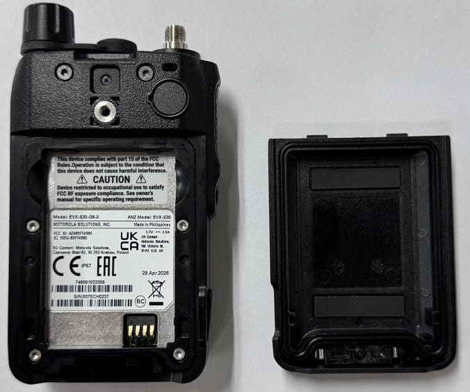
AZ489FT4980
Sep 08, 2026Portable two way radio
Equipment Class
TNF - Licensed Non-Broadcast Transmitter Held to FaceAZ489FT4981
Aug 14, 2026Handheld Portable - TANAPA BPR 45 400-470 MHZ 4W NKP
Equipment Class
TNF - Licensed Non-Broadcast Transmitter Held to Face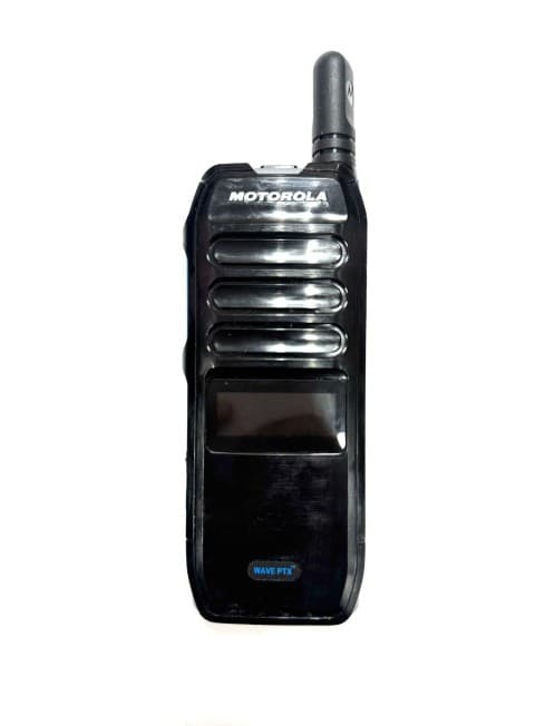
AZ489FT7187
Jul 13, 2026Portable 2-Way Radio with Bluetooth, Bluetooth LE, WIFI 2.4GHz, WIFI 5GHz, LTE
Equipment Class
DSS - Part 15 Spread Spectrum TransmitterAZ499FT6031
May 11, 2026Operation Critical Wireless Earpiece PTT
Equipment Class
DSS - Part 15 Spread Spectrum Transmitter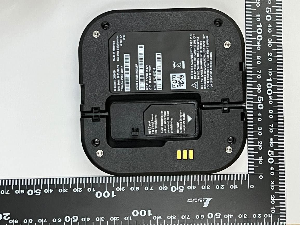
AZ499FT5879
Dec 19, 20252-way Portable Radio with BT, BTLE, WIFI, NFC and LTE
Equipment Class
DSS - Part 15 Spread Spectrum Transmitter