AZ489FT4832
Motorola Solutions, Inc.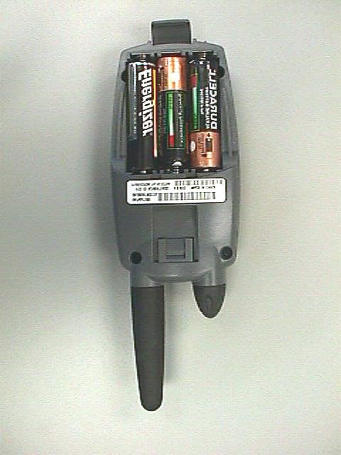
Click to zoom
Application Details
- Equipment Class
- FRF - Part 95 Family Radio Face Held Transmitter
- Date of Grant
- Apr 11, 1999
- Application Purpose
- Original Equipment
- Date of Application
- Mar 22, 1999
- Frequency Range
- 462.56250000 - 467.71250000
- Company
- Motorola Solutions, Inc.
- Country
- United States
Documents & Files
Document Text
Text extracted from the exhibit documents filed with the FCC. Open a document above to read the original.
Users Manual
Applicant: Motorola Inc FCC ID: AZ489FT4832 INSTRUCTION MANUAL X Preliminary Manual attached. Complete Manual attached. EXHIBIT 8 Applicant: Motorola Inc FCC ID: AZ489FT4832 Let’s Talk About Your New Radio Motorola FR50 radios operate on Family Radio Service (FRS) designated frequencies. This license-free, short range, two-way radio service was established specifically for family and group recreational use. You can use your radios anywhere within the United States and other areas listed by the FCC. Contact the FCC for more information. Batteries FR50 radios operate with 3 AA alkaline batteries providing approximately 30 hours of use. That’s about 3 hours of talk and 27 hours of standby time. To Install: 1.With the back of the radio facing you, flip the battery door clip down to release door. 2.Lift door off. 3.Insert 3 AA batteries making sure the plus signs are aligned on batteries and in the battery chamber. 4.Replace the battery cover. 5.Reposition the battery door clip and snap into place. Low Battery Alert: When batteries are low, the radio will chirp 1 to 2 seconds after turning power on, every 10 minutes, and after release of the Push-To-Talk button. Replace the batteries immediately to avoid interrupted use. Note: Remove batteries before storing your radio for extended periods. Batteries corrode over time and may cause permanent damage to your radio. Belt Clip Motorola FR50 radios come standard with a belt clip. To Attach: 1.Locate the belt clip attachment opening on the radio’s back. 2.Align the belt clip with the grooves in the radio back. 3.Gently push up until it clicks into place. To Remove: 1. Grasp radio firmly. 1. Pull belt clip up and off the radio back. Before You Can Talk Read this manual carefully, make sure you know how to properly operate the radio before use. Motorola FR50 radios have 14 channels. To talk to others, all radios in your group must be set to the same channel (see charts in “Appendix A”). Turn the Radio On: 1.Rotate Power/Volume knob until you hear a click. The radio will beep to confirm. The display will show the current channel. 2.To turn radio off, Rotate Power/Volume knob until you hear a click and display disappears. Set the Channel 1. Turn the radio on. 1. Press Menu button. Current channel will begin to flash. Applicant: Motorola Inc FCC ID: AZ489FT4832 1. Use scroll buttons to set a new channel. The new channel will flash. 1. Press Menu button to set new channel. To Communicate Monitor Button: The Monitor button is used to check activity on current channel before transmitting. It also lets you hear the radio’s volume level when you’re not receiving so you can adjust the volume. Radio Etiquette: Your radio’s 14 channels are shared on a “take turns” basis. This means other groups may be talking on the channels. For uninterrupted communications, follow the steps below: 1.Use the Monitor button to check activity on the channel before talking. 2.Don’t talk over someone who is already using the channel – your message may not be completely heard. Try changing the Channel to avoid channel congestion. Note: Since the channels are shared, your conversations will not be private and you may hear others talking. Adjust the Volume: Rotate Volume knob until you reach a comfortable listening level. Rotate knob clockwise to increase and counter clockwise to decrease volume. Sending Messages: 1.Check channel activity by pressing Monitor button, you’ll hear static if the channel is clear to use. Don’t transmit if someone’s talking on the channel. 2.To maximize clarity, hold radio 2 to 5 inches from mouth. Press Push-To-Talk button and speak into radio. The LED Indicator Light glows continuously when transmitting. To receive messages, release the Push-To-Talk button. Time-out Timer: The Time-out Timer feature helps extend battery life. The radio will emit a continuous warning tone if the Push- To-Talk button is pressed for 60 continuous seconds and will stop transmitting. Call Tone Call Tones identify sender and alert receiver. Press the Call button and users on your channel will be alerted with your Call Tone. To Use Call Tone: 1. Turn radio on. 1. Press Call button. Compander Feature: FR50 radios have a built-in voice compander that enhances the audio quality, creating crystal clear communications. Talk Range Motorola FR50 radios have been designed to maximize performance and improve transmission range in the field. It is recommended that you do not use the radios closer than 5 feet apart because of heavy interference. Applicant: Motorola Inc FCC ID: AZ489FT4832 Optimal Range: Maximum talk range in flat, open areas, for up to 2 (two) miles. Medium Range: Range is decreased when buildings and trees are in the way. Minimal Range: Dense foliage and mountains can limit range. Care of Your Radio To clean the radio, wipe with a soft cloth dampened with water. Don’t use cleaners or solvents on the radio, they can harm the body and leak inside, causing permanent damage. Battery contacts may be wiped with a dry, lint-free cloth. If the radio gets wet, turn it off and remove batteries immediately. Dry battery compartment with a soft cloth to minimize potential water damage. Leave cover off the battery compartment overnight or until completely dry. Do not use the radio until completely dry. Frequently Asked Questions Will FR50 radios work with other two-way radios? Radios operating on the same frequency can communicate with each other. Radios with Interference Eliminator codes must have the codes off to talk to FR50 radios. Why are there so many channels? The more channels, the less channel congestion. If people use the radios in congested areas, i.e. malls, zoos, ski areas, the choice of more channels reduces interrupted communications. If you hear other conversations, simply change your channel to find a less busy channel to talk on. How many radios can communicate in the same group? As many as you want, as long as the radios are set to the same channel and code (or code…
Text truncated - open the document above for the full version.
Attestation Statements
FCC ID: AZ489FT4832 STATEMENT OF CERTIFICATION The technical data supplied with this application, having been taken under my supervision is hereby duly certified. The following is a statement of my qualifications: 1) B.S.E.E. from the University of Miami. 2) M.S.E.E from Florida Atlantic University. 3) 2 years of Design and Development experience in the field of two-way radio communications. Name: Joe Zbib Signature: Joe Zbib (signed) Date: March 18,1999 . Position: Electrical Dev. Engineer I hereby certify that the above application was prepared under my direction and that to the best of my knowledge and belief, the facts set forth in the application and accompanying technical data are true and correct: Name: Mark Bradford Signature: Mark Bradford (signed) Date: March 18,1999 Position: Senior Resource Manager EXHIBIT 2
Block Diagram
Applicant: Motorola Inc FCC ID: AZ489FT4832 BLOCK DIAGRAMS A general description of the overall circuit is not covered in an instruction manual. This section provides the description of circuits required by subpart 2.983 of the Commissions’ rules. Circuits not described in the manual are covered in this exhibit. The following are included: 1. Means for Frequency Stabilization4A 2. Means for Modulation Limiting4B and Low Pass Filter 3. Means for Harmonic Suppression4C 4. Means for Limiting Power4D EXHIBIT 4 Applicant: Motorola Inc FCC ID: AZ489FT4832 CARRIER FREQUENCY GENERATION AND STABILIZATION CIRCUIT DESCRIPTION: The carrier frequency is generated using frequency synthesizer IC102 with an external voltage controlled oscillator (VCO) composed of active element Q103, tunable inductor L106 and varactor D102 and associated bias and filtering components. The reference frequency for the synthesizer is set at 12.8 MHz by X-OSC01 a 2.5 ppm temperature compensated crystal oscillator. The oscillator operates off a regulated voltage to minimize frequency variations with battery voltage. Transistor Q106 and PIN diode D103 is used to range shift the VCO between transmit and receive frequencies. The VCO operates at one half the desired frequency and discrete components are used select the second harmonic for the transmit power amplifier and the receiver local oscillator. Transmitter modulation is applied to PIN diode D103 through variable resistor VR102. For circuit diagram refer to the schematic in Exhibit 5. EXHIBIT 4A Applicant: Motorola Inc FCC ID: AZ489FT4832 MODULATION LIMITING AND LOW PASS FILTER BLOCK DIAGRAMS: Microphone audio is generated in audio transducer MIC101 or applied from an external audio accessory through accessory jack CN101. This signal is then high pass filtered using IC104A and discrete components. This filtered signal is then compressed by compander IC103 and pre- emphasized and limited by IC104B and associated discrete components. Q109 and associated discrete components provide a 3 pole low pass filter with a corner frequency of 3 kHz to filter the limiter output. Variable resistor VR102 is used to set the maximum deviation to 2.4 kHz. PIN diode D103 is used to couple the modulation signal into the VCO. For circuit diagram refer to the schematic in Exhibit 5. EXHIBIT 4 B Applicant: Motorola Inc FCC ID: AZ489FT4832 HARMONIC SUPPRESSION CIRCUIT CIRCUIT DESCRIPTION: . The output of the transmit power amplifier is followed by a combination matching network and low pass filter to attenuate harmonics from the amplifier and PIN diode based antenna switch. The matching and low pass filter is composed of C148, L111, C149, C150, C151, L112, C152 and C153. Bias for the PIN diode antenna switch (D104 and D101) is provided by L110 and R127. For circuit diagram refer to the schematic in Exhibit 5. EXHIBIT 4C Applicant: Motorola Inc FCC ID: AZ489FT4832 MEANS FOR LIMITING POWER CIRCUIT DESCRIPTION The transmit power amplifier is a two stage discrete design. The driver stage uses a Toshiba 2SC5087 bipolar transistor (Q104) with an input drive of about 0 dBm and an output power of about 18 dBm. The output stage uses a Toshiba 2SK3078 FET (Q105) with an output power of about 27 dBm. The output stage is followed by a low pass filter, a PIN diode antenna switch and a permanently attached antenna. The output power is not adjustable and is set by discrete components in the power amplifier. For circuit diagram refer to the schematic in Exhibit 5. EXHIBIT 4D
Cover Letter(s)
FCC ID: AZ489FT4832 Radio Products Group 8000 West Sunrise Boulevard, Fort Lauderdale, Florida 33322. (954)723-5000 Date: March 23, 1999. Authorization and Evaluation Division Federal Communications Commission Laboratory 7435 Oakland Mills Road Columbia. MD 21046 Att:Frank Coperich, George Tannahill Subject: Application for Certification of Transmitter with FCC ID: AZ489FT4832. Gentlemen: Motorola Inc, 8000 West Sunrise Boulevard, Fort Lauderdale, Florida, herein submits application for Certification of the subject transmitter. This transmitter is primarily intended for use in the Family Radio Service (FRS) application with capabilities for clear communications with transmit output power of 0.5 Watt or 27 dBm. The subject transmitter complies with Section 90.203 of the rules in that the operator cannot directly program transmit frequencies using only the unit’s normally accessible external controls. Enclosed is a complete Type Acceptance Application. Contact me (954) 723-5793 or Fax me at (954) 723-4794, if you require any additional information. Sincerely, Mike Ramnath. FCC Liaison.
External Photos
Applicant: Motorola Inc FCC ID: AZ489FT4832 EXTERNAL PHOTOGRAPHS Front view of Radio EXHIBIT 3-1 Applicant: Motorola Inc FCC ID: AZ489FT4832 Rear view of Radio showing FCC ID location. EXHIBIT 3-2 Applicant: Motorola Inc FCC ID: AZ489FT4832 Magnified view of FCC ID. EXHIBIT 3-3 Applicant: Motorola Inc FCC ID: AZ489FT4832 Rear view of Radio with battery cover removed. EXHIBIT 3-4
ID Label/Location Info
Applicant: Motorola Inc FCC ID: AZ489FT4832 LIST OF EXHIBITS DESCRIPTION EXHIBIT REFERENCE I. Identification label information12.983-(f) & General Information1a 1. Production Plans2.981-(a) 2. Application References2.1061 3. Data Submittal Procedure 4. Similar Applications II. Certification of Data2 III. External Photographs32.983-(g) IV. Block Diagrams4 1. Frequency Stabilizing4A 2. Modulation Limiting4B and Post Limiter Filter 3.Harmonic Suppression 4C 4.Power Limiting4D V. Schematic Diagrams52.983-(d)-7 VI. Test Report6 1. Data Index6 2. RF Output Data6A2.985 3. Modulation Characteristics2.987 A. Audio Response & Low Pass Filter Response6B, 9C B. Modulation Limiting6D 4. Occupied Bandwidth6E2.989 5. Conducted Spurious Emissions 6F2.991 6. Radiated Spurious Emissions6G2.993 7. Frequency Stability (Temperature & Supply Voltage)6H-1, 9H-22.995 8. Transient Frequency Behavior6I90.214 VII. Test Set-up Procedures72.999 VIII. Instruction Manual8 2.983-(d)-8 IX. Internal Photographs.9 2.983-(g) X. Parts List and Tune-Up procedures102.983-(d)-6, 9 XI. RF Exposure Information112.1093 XII. Operational Description12 2.983- (d)1,2,3,4,5 1. Technical Characteristics 2. Application XIII. Cover Letter13 Applicant: Motorola Inc FCC ID: AZ489FT4832 IDENTIFICATION LABEL LOCATION X See The Attached Photograph Or Sketch Back Of Radio Back Of Radio Under Belt Clip TYPE X The label is a paper polyester film laminate with a pressure sensitive adhesive backing. The adhesive is a permanent type acrylic with a minimum peel strength of 40 oz/ inch. The label is laser etched into the Urethane paint, exposing the Nickel plating on the Zamak casting substrate. Since no adhesive is required, the label is permanent and tamper-proof. (** - NOTE- The label attached below is a paper polyester film laminate, as described above. This is just for sample purposes, as the actual label is laser etched into the casting) MARKINGS (TEXT) See the attached Photograph, Exhibit 3. EXHIBIT 1 Applicant: Motorola Inc FCC ID: AZ489FT4832 GENERAL INFORMATION I.Production Plans—Pursuant 2.983 ( c ). Quantity production is planned. II.Application References -- Pursuant 2.1061 Reference is made to the following Motorola “Application References” 1. Portable Products and their application. 2. Portable Products Transmitter Modulations Methods. III.Data Submittal Procedure: Data is supplied in accordance with Part 2, Sub-part J of the Commissions’ Rules. IV.Similar, currently Type Accepted Transmitter, FCC ID: AZ489FT4818. EXHIBIT 1a
Internal Photos
Applicant: Motorola Inc FCC ID: AZ489FT4832 INTERNAL PHOTOGRAPHS Front View of Main Board. EXHIBIT 9-1 Applicant: Motorola Inc FCC ID: AZ489FT4832 Back view of Main Board. EXHIBIT 9-2
Operational Description
Applicant: Motorola Inc FCC ID: AZ489FT4832 OPERATIONAL DESCRIPTION I.Transmitter Technical Characteristics—Pursuant 2.983 (d) A. RF Power Output0.5 Watt B. Frequency Range 462.5625 - 467.7125 MHz C. Frequency Stability 0.00025 % D. Emissions 11K0F3E, (see General Info. ) E. Spurious Emissions 76.1dBc F. DC Voltage and Current into 4.5 Volts the final RF amplifier stage/stages 450 mAmps II.Transmitter Application This transmitter is primarily intended for use in a hand-held two-way portable radio. The radio is characterized by the following features, options and accessories. A.Power Supply Available 1. NiCad Battery , Mercury Battery , Alkaline Battery X , AC , Lead Acid Battery , Nickel Metal Hydride . B.Antenna Available 1. Helical X , Telescopic , Whip , Dipole , Dribble External _________, External __________. C.Squelch Types Available 1. Carrier Squelch X . 2. Tone “Private Line” . 3. Digital “Private Line” . D.Microphone - Control 1. Handset/Palm Microphone X . 2. 600 Ohm wireline control . E.Maximum Transmit Channel Capability 14 . F.Housing The transmitter will be housed in the housing shown in the accompanying photographs. G.Other Options 1. Single Tone Encoder N/A 2. Multiple Single Tone Encoder N/A 3. Touch Code Encoder N/A 4. Unit ID Encoder N/A 5. EMS Telemetry Encoder N/A 6. Time out Timer X 7. Voice EncryptionN/A 8. Digital Signaling N/A 9. Sel-Call Decode N/A 10. Trunking N/A EXHIBIT 12
Parts List/Tune Up Info
Applicant: Motorola Inc FCC ID:AZ489FT4832 PARTS LIST AND TUNE-UP PROCEDURE REFERENCEDESCRIPTIONVENDORVENDOR P/N D101,D103PIN DIODE 1SS314TOSHIBA1SS314 D102DIODE VARACTOR 1SV214TOSHIBA1SV214 D104PIN DIODE BAR63-03WSIEMENSBAR63-03W D105SILICON DUAL DIODE ARRAYSROHMDA204K D106SCHOTTKY DIODESROHMRB425D Q101TR CHIP NPN 2SC4226R24NEC2SC4226R24 Q102TR.CHIP FET DUAL GATE 3SK320TOSHIBA3SK320 Q103TR CHIP HN3C10FTTOSHIBAHN3C10FT Q104TR CHIP 2SC5087COTOSHIBA2SC5087CO Q105TR. CHIP FET 2SK3078TOSHIBA2SK3078 Q106, Q112TR CHIP NPN 2SC27122SC2712 Q107, Q108, Q111 TR DIGITAL CHIP PNP DTA143EKAROHMDTA143EKA Q109N-CHANNEL J-FET 2SK303SANYO2SK303 Q110TR DIGITAL CHIP NPN DTC114EKAROHMDTC114EKA BPF101SAW FILTER 465.1375MHZ SAMSUNGSAMSUNGS465PC BPF102CRYSTAL FILTER 26.05MHZ KSSKSSMXF 26.05-15A6 BPF103CERAMIC FILTER 450 kHz MURATAMURATACFW450G IC101IC DBL5019V IF SYSTEMDAEWOODBL5019V IC102IC M64082AGP PLL ICMITSUBISH I M64082AGP IC103COMPANDER IC DBL5020V SOPDAEWOODBL5020V IC104IC KA358D LOW POWER DUAL OP AMP SOP SAMSUNGKA358D IC105IC RECEIVER AMP MC34119D-R2MOTOROL A MC34119 IC106CMOS MICROCONTROLLERTOSHIBATMP87C405M IC107IC XC62AP3002PR 3V REGULATOR SOT89TOREXXC62AP3002PR IC1083.3V DETECTOR S-80733AN-DX-X(SOT-89- 3) SEIKOS-80733AN-DX-X IC201RAM MAPPING 32X4 LCD CONTROLLERHOTEXHT1621B X0SC0112.8MHZ KXN1292A MOTOROLA TCXOMOTOROL A KXN1292A X0SC02CRYSTAL 4.194304MHZ CSA-309 CITIZENCITIZENCSA-310 EXHIBIT 10 Applicant: Motorola Inc FCC ID:AZ489FT4832 TUNE UP PROCEDURE The following tune-up procedure is for the factory only. There will be no customer tuning. Tuning Procedures ALIGNMENT (PCB level) (Test Condition: under CH1) NO.ITEMALIGNMENT METHODREMARK 1.Standby current1. Set A-METER, and RX mode 2. Check the standby current <45mA VDC 2.RX Current @ Rated 1. Set SG RF level to –50dBm with 1.5kHz deviation at 1kHz audio frequency. 2. Rotate the volume switch to the position, which give an output 900mV at TP14. 3. Check the RX current <200mA 3.Talk on current1. Set A-METER, and TX mode 2. Check the talk on current <500mA DC 4.Tx VCO1. Set TX mode 2. Adjust L106 to provide 2.4 VDC at TP04 on CH14 3. Check TP04 to provide 0.5 ~ 1.2 VDC on CH1 5.Rx VCO1. Set RX mode on CH1 2. Check TP04 to provide 0.5 ~ 1.2 VDC on CH1 3.Check TP04 to provide 1.5 ~ 2.5 VDC on CH14 6.Tx Power1. Set TX mode 2. Check transmit power to provide 26 ~ 27.5dBm 7.Tx Frequency1. Adjust VR103 to provide 462.5625MHz ± 300Hz 8.Tx Modulation & distortion 1. Input 55mV 1000Hz at TP05 2. Adjust VR102 to provide max TX deviation 2.4kHz. 3. Check normal deviation @ input 5.5mV 1kHz audio frequency to be >1kHz and <2kHz. 4. Check the demodulation distortion <= 3.5% 5. Audio Frequency Response a) Input a 2.0mV 1KHz audio frequency to TP05 and press ‘PTT’ switch. b) Check the response compare to 1kHz tone i) 300Hz (-9.5 to –13.5)dB. Applicant: Motorola Inc FCC ID:AZ489FT4832 ii) 3kHz (+6.5 to +10.5)dB iii) 6kHz (-17 to –21)dB 9.Rx Sensitivity1. Reduce SG RF level 2. Check SINAD sens. <= -118dBm @12dBSINAD at TP14 10.Rx Audio1. Set RX mode 2. Set SG RF level to -50dBm with 1.5 kHz dev. 1KHz mod. sig. 4. Adjust T101 to provide min. distortion 5. Check audio output >100mV at TP10 6. Check the 1kHz distortion <= 3.5% 7. Audio frequency response a) Set SG RF level to –50dBm with 0.5kHz deviation at 1kHz audio frequency. b) Rotate the volume switch to the position, which give an output 200mV (±5mV) at TP14. c) Vary the audio frequency from 300Hz – 3KHz. d) Check the RX response compare to 1KHz tone. i) 300Hz (+15 to +23)dB ii) 3KHz (-17 to –25)dB 8. Maximum and Minimum Audio Output Power a) Set SG RF level to –40dBm with 1.5kHz deviation at 1KHz audio frequency. b) Rotate the volume switch to the position, which give a maximum output with distortion <5%. c) Check the voltage at TP14 >800mV d) Set maximum audio output to 0dB, rotate the volume switch to the position, which give a minimum output. Check the min. voltage at TP14 (-35dB ±5dB) 11.RSSI Detector1. Set SG to -119dBm with 1.5kHz dev., 1kHz tone on CH7 2. Adjust VR101 for HIGH state : 9dBSINAD 3. Check for LOW state : 4dBSINAD 4. Repeat on CH8 12.Battery Detect 1. Low Battery, 3.4V (speaker output beep tone and indicate LED flash). 2. Dead Battery, 3.0V (to be define by customer). * Remark: Applicant: Motorola Inc FCC ID:AZ489FT4832 TX mode : 1. Press and hold PTT button RX mode : 1. Release PTT button TESTING (Casing) NO.ITEMTEST METHODREMARK 1.Current Consumption 1. Set A-METER, plug the dummy speaker and dummy mic into audio jet. 2. With volume switch OFF, check the OFF current <10mA. 3. With volume switch ON, check the standby current <45mA. 4. RX Current @ Rated a) Set SG RF level to –40dBm with 1.5kHz deviation at 1kHz audio frequency. b) Rotate the volume switch to the position, which give an output 900mV ±50mV (voltage difference of dummy speaker). c) Check the RX current <200mA. 1. TX Current a) Input a 5.5mV 1kHz audio frequency to dummy mic. b) Press ‘PTT’ switch and check the TX current <500mA. 2.Battery Detect 1. Low Battery, 3.3V (speaker output beep tone and indicate LED flash). 2. Dead Battery, 3.0V (to be define by customer). 3.Audio RX Path1. Plug the dummy speaker and dummy mic into audio jet. 2. Check the radiated sensitivity correlate to the golden sample 3. Audio frequency response a) Set SG RF level to –40dBm with 0.5kHz deviation at 1KHz audio frequency. b) Rotate the volume switch to the position, which give an output 50mV (±5mV) (voltage difference of dummy speaker). c) Vary the audio frequency from 300Hz – 3kHz. d) Check the RX response compare to 1kHz Applicant: Motorola Inc FCC ID:AZ489FT4832 tone. e) 300Hz (+15 to +23)dB ii) 3KHz (-17 to –25)dB 1. Maximum and Minimum Audio Output Power a) Set SG RF level to –40dBm with 1.5kHz deviation at 1KHz audio frequency. b) Rotate the volume switch to the position, which give a maximum output with distortion <5%. c) Check the voltage difference of dummy speaker >775mV. d) Set maximum audio output to 0dB, rotate the volume switch to the p…
Text truncated - open the document above for the full version.
RF Exposure Info
Applicant: Motorola Inc FCC ID: AZ489FT4832 RF EXPOSURE INFORMATION: In accordance with 47 CFR 2.1093 (c), this transmitter has been subjected to routine environmental evaluation for RF exposure and found to be compliant with the limits specified in 47 CFR 2.1093 (d). EXHIBIT 11
Schematics
Applicant: Motorola Inc FCC ID: AZ489FT4832 SCHEMATIC DIAGRAMS The following schematic diagrams show circuit connectivity. EXHIBIT 5
Test Report
Applicant: Motorola Inc FCC ID : AZ489FT4832 TEST REPORT MEASUREMENT EXHIBIT NUMBER OF PAGES I RF Power Output6A1-22 IIAudio Response6B1 IIILow Pass Filter Response6C1 IVModulation Limiting A. 12.5 kHz channel spacing case6D1 VOccupied Bandwidth6E -12 VIConducted Spurious Emissions6F 1-22 VIIRadiated Spurious Emissions2 A. Tx Vertical – 0.5 Watt6G B. Tx Horizontal – 0.5 Watt6G VIII Frequency Stability A. Temperature6H-11 B. Supply Voltage 6H-21 EXHIBIT 6 Applicant: Motorola Inc FCC ID : AZ489FT4832 RF POWER OUTPUT DATA The RF power output was measured with the indicated voltage applied to and current into the final RF amplifying device. 0.5 Watt Measured RF output.505Watts Nominal DC Voltage4.0Volts Nominal DC Current450mA Primary Supply Voltage4.0Volts Effective Radiated Power (ERP)*26.3dBm • This is a calculated number from graph 6A-1 where it shows an ERP of –11.6 dBm and the anechoic chamber’s path loss was measured to be 37.9 dBm. EXHIBIT: 6A-1 Applicant: Motorola Inc FCC ID : AZ489FT4832 Exhibit 6A-2 FCC ID: AZ489FT4832 EXHIBIT 6B Audio Frequency Response -25-20-15-10 -5 05 1015 100 1000 10000 Frequency(Hz) Amplitude(dB datahigh speclow spec FCC ID: AZ489FT4832 From 10 kHz to 20 kHz was in the noise floor of instrument. EXHIBIT 6C FR50 TX LP Response -50-40-30-20-10 0 10 300 500 700 100 0 1500 2000 250 0 3000 3500 4000 5000 600 0 7000 8000 100 00 12000 14000 16000 20000 Fr e q ue n cy ( Hz ) Amplitude (dB) Series1 FCC ID: AZ489FT4832 EXHIBIT 6D Modlimiting Vs. Amplitude 0 500 10001500200025003000 -25 -20 -15 -10 -5 0 5 10 15 20 25 Amplitude(dB) Deviation(Hz 300 Hz1 KHz3 KHzspec FCC ID: AZ489FT4832 OCCUPIED BANDWIDTH DATA 12.5 kHz Channel Spacing EXHIBIT 6E-2 2500 Hz Audio ModulationEmission Type: 11K0F3EHorizontal: 10 kHz/Div.Vertical: 10 dB/Div.Carrier Ref: 0 dBSpecification Mask per FCC Rule Part 95.635. CARSON’S RULE11K0F3E:BW = 2(M + D)BW = 2 (3 kHz maximum modulation frequency + 2.5 kHz deviation)BW = 2 (5.5)BW = 11 kHz EXHIBIT 6E-1 FCC ID: AZ489FT4832 EXHIBIT 6E-2 FCC ID: AZ489FT4832 EXHIBIT 6F-1 FCC ID: AZ489FT4832 E XHIBIT 6F-2 Applicant: Motorola Inc FCC ID: AZ489FT4833 Transmitter Radiated Spurious Emissions: FR50 467.5625 MHz - 0.5 W - 12.5 kHz CH. Spacing Horizontally Polarized Frequency (MHz) FCC Maximum Emission Limit (dBm) 12.5 kHz Ch. Spac. Measured Emission Equivalent Power Into an Ideal Dipole (dBm) 2X FUND935.1250-20* 3X FUND1402.6875-20-49.4 4X FUND1870.2500-20-42.7 5X FUND2337.8125-20-37.7 6X FUND2805.3750-20-39.4 7X FUND3272.9375-20-37.3 8X FUND3740.5000-20-34.6 9X FUND4208.0625-20-40.2 10XFUND4675.6250-20-37.4 Verticall y polarized Frequency (MHz) FCC Maximum Emission Limit (dBm) 12.5 kHz Ch. Spac. Measured Emission Equivalent Power Into an Ideal Dipole (dBm) 2X FUND935.1250 -20* 3X FUND1402.6875 -20-49.1 4X FUND1870.2500 -20-42.7 5X FUND2337.8125 -20-33.7 6X FUND2805.3750 -20-40.3 7X FUND3272.9375 -20-38.1 8X FUND3740.5000 -20-33.4 9X FUND4208.0625 -20-39.1 10XFUND4675.6250 -20-39.6 * Indicates the spurious emission was less than -60dBm or could not be detected due to noise limitations or ambients. Exhibit 6G Radiated Transmitter Emissions Vertically Polarized Antenna -60.0 -50.0 -40.0 -30.0 -20.0 -10.0 0.0 935 . 1250 14 02. 6875 1870. 2500 23 37. 8125 2805 . 3750 32 72. 9375 3740 . 5000 4208.0625 467 5. 6250 Frequency (MHz) Emission Level (dBm) Measured Emission Equivalent Power Into an Ideal Dipole (dBm) FCC Maximum Emission Limit (dBm) 12.5 kHz Ch. Spac. Radiated Transmitter Emissions Horizontally Polarized Antenna -60.0 -50.0 -40.0 -30.0 -20.0 -10.0 0.0 93 5. 1250 1402.6875 1870. 2 500 2337. 8 125 2805. 3 750 3272. 9 375 3740.5000 4208. 0625 4675. 6250 Frequency (MHz) Emission Level (dBm) Measured Emission Equivalent Power Into an Ideal Dipole (dBm) FCC Maximum Emission Limit (dBm) 12.5 kHz Ch. Spac. Applicant: Motorola Inc FCC ID: AZ489FT4833 Radio resets at 3.3 Volts. EXHIBIT 6H-1 Frequency Stability over Temperature -2000-1000 0 10002000 -20 -20 -10 0 10 20 30 40 50 60 Te mp°C Hz Fre q Errlos pe cups pe c Applicant: Motorola Inc FCC ID: AZ489FT4833 EXHIBIT 6H-2 Frequency Error over Voltage (ppm) -3-2-1 0123 3 3.2 3.4 3.6 3.8 4 4.2 4.4 4.6 Supply Voltage(V) Frequency Error(ppm Freq Error (ppm )upper speclower spec
Test Setup Photos
Applicant: Motorola Inc FCC ID: AZ489FT4832 TEST SET- UP PROCEDURES Except where otherwise stated, all measurements are made following the Electronic Industries Association (EIA) Minimum Standard for Portable/Personal Land Mobile Communications FM or PM Equipment 25-1000 MHz-(TIA/EIA-603). This exhibit presents a brief summary of how the measurements were made, the required limits, and the test equipment used. The following procedures are presented with this application. 1.RF Power Output X 2.Audio Response X 3.Low Pass Filter Response X 4.Modulation Limiting X 5.Occupied Bandwidth X 6.Radiated Spurious Emissions X 7.Conducted Spurious Emissions X 8.Frequency Stability X EXHIBIT 7 Applicant: Motorola Inc FCC ID: AZ489FT4832 TEST EQUIPMENT LIST Pursuant To FCC Rules 2.999 1. Spectrum Analyzer A. HP 8591E B. HP 8566 C. HP35665A 2. RF Signal Generators A. HP 8665 B. HP 8642 C. HP 8656 3. RF Millivoltmeter A. Boonton 4200 B. Boonton 4210 4. RF Loads A. WEINSCHEL M1418 5. Dipole Antenna Set A. Singer DM-105A series B. EMCO Model 3120 6. RF Power Meters A. HP 436A B. 8482B Power Sensor C. 30 dB High Power Pad 7. Monitor Receivers A. Motorola Comm Syst Analyzer B. HP8901 8. Tenny Temperature Chamber 9. Frequency Counters a. HP 5385A 10. Audio Analyzer a. HP8903B 11. AC/DC Voltmeters a. Fluke8012A Digital Multimeter 12. HP8901B Modulation Analyzer EXHIBIT 7 Applicant: Motorola Inc FCC ID: AZ489FT4832 RF POWER OUTPUT Pursuant to FCC Rules 2.985 (a) Method of Measurement The RF power output is measured with the value of voltage and current specified in Exhibit 3 as required by 2.983(d) (5). A 50 ohm RF attenuator of proper power rating was used as a load for making these measurements. For Transmitter having an output impedance other than 50 ohm, a suitable matching network is placed between the transmitter and the load. The power measurements are made using a Hewlett Packard series HP 436A power meter and 30 dB attenuator or a HP 437B power meter. AUDIO FREQUENCY RESPONSE Pursuant FCC Rules 2.987 (a) Method of Measurement Operate the transmitter under standard test conditions and monitor the output with a frequency deviation meter or calibrated test receiver. With 1000 Hz sine wave audio input applied through a dummy microphone circuit, adjust the audio input to give 30% of full rated system deviation Maintaining constant deviation, vary the input frequency from 100 to 5000 Hz, and observe the level necessary to maintain a constant 30% modulation. Minimum Standard The audio frequency response shall not vary more than +1 or -3 dB from 300 to 3000 Hz as referenced to 1000 Hz level (with the exception of a permissible 6 dB/octave roll off from 2500 to 3000 Hz) POST LIMITER FILTER FREQUENCY RESPONSE Pursuant FCC Rules 2.987 (a) Method of Measurement An audio signal was injected into the post limiter low pass filter The output of the limiter was measured via a test pin with a dynamic signal analyzer(HP35665). A 1 kHz tone was injected and this output level was used as reference (0 dB). The input was varied from 1000 Hz to 30,000 Hz and the change in output was measured. EXHIBIT 7 Applicant: Motorola Inc FCC ID: AZ489FT4832 MODULATION LIMITING Pursuant FCC Rules 2.987 (a) Method of Measurement The transmitter shall be adjusted for full rated system deviation. Adjust the audio input for 60% of rated system deviation at 1000 Hz. Using this level as a reference (0 …
Text truncated - open the document above for the full version.
Contact Information
Applicant
Deanna Zakharia(Regulatory Compliance Manager)
Technical Contact
Motorola IncMike Ramnath
[email protected]954-723-5793
8000 West Sunrise Blvd · Fort Lauderdale, Florida · United States
Technical Specifications
| # | Rule Parts | Frequency Range | Power Output | Tolerance |
|---|---|---|---|---|
| 1 | 95 | 462.5625 MHz - 467.7125 MHz | 500.00 mW | ppm |
Other Applications from Motorola Solutions, Inc.
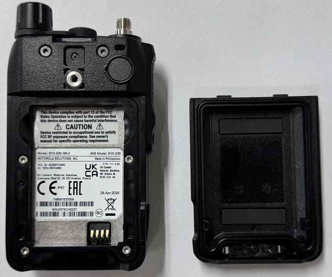
AZ489FT4980
Sep 08, 2026Portable two way radio
Equipment Class
TNF - Licensed Non-Broadcast Transmitter Held to FaceAZ489FT4981
Aug 14, 2026Handheld Portable - TANAPA BPR 45 400-470 MHZ 4W NKP
Equipment Class
TNF - Licensed Non-Broadcast Transmitter Held to Face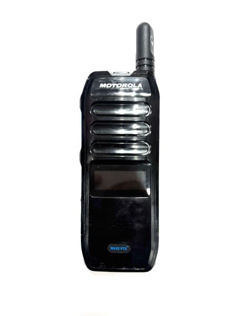
AZ489FT7187
Jul 13, 2026Portable 2-Way Radio with Bluetooth, Bluetooth LE, WIFI 2.4GHz, WIFI 5GHz, LTE
Equipment Class
DSS - Part 15 Spread Spectrum TransmitterAZ499FT6031
May 11, 2026Operation Critical Wireless Earpiece PTT
Equipment Class
DSS - Part 15 Spread Spectrum Transmitter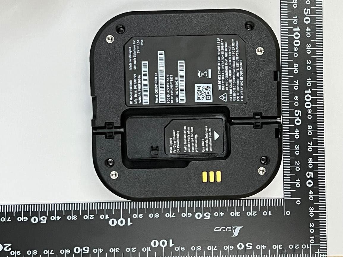
AZ499FT5879
Dec 19, 20252-way Portable Radio with BT, BTLE, WIFI, NFC and LTE
Equipment Class
DSS - Part 15 Spread Spectrum Transmitter