AZ489FT4834Hand-held Transmitter
Motorola Solutions, Inc.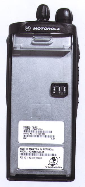
Click to zoom
Application Details
- Equipment Class
- TNF - Licensed Non-Broadcast Transmitter Held to Face
- Date of Grant
- Apr 25, 1999
- Application Purpose
- Original Equipment
- Date of Application
- Mar 01, 1999
- Equipment Note
- Hand-held Transmitter
- Frequency Range
- 450.00000000 - 512.00000000
- Company
- Motorola Solutions, Inc.
- Country
- United States
Documents & Files
Document Text
Text extracted from the exhibit documents filed with the FCC. Open a document above to read the original.
Users Manual
1 Copyright Information The Motorola products described in this manual may include copyrighted Motorola computer programs stored in semiconductor memories or other mediums. Laws in the United States and other countries preserve for Motorola certain exclusive rights for copyrighted computer programs, including the exclusive right to copy or reproduce in any form the copyrighted computer program. Accordingly, any copyrighted Motorola computer programs con-tained in the Motorola products described in this instruction manual may not be copied or reproduced in any man-ner without the express written permission of Motorola. Furthermore, the purchase of Motorola products shall not be deemed to grant either directly or by implication, estoppel, or otherwise, any license under the copyrights, pat-ents, or patent applications of Motorola, except for the normal non-exclusive, royalty free license to use that arises by operation of law in the sale of a product.© 1998 by Motorola, Inc.All Rights Reserved.Motorola Malaysia Sdn. Bhd. (Company No. 12631DE),Bayan Lepas Free Industrial Zone, Phase 3,11900 Penang, Malaysia.Printed in Malaysia. , Motorola, Call Alert and MDC are trademarks of Motorola, Inc. GP328 Quic k Ref erence Car d Deleting a Nuisance Channel1. While r adio is on a Nuisance Channel, press and hold Scan b utton until a tone is sounded. 2. Release Scan b utton. For K e ypad Radios onl y Making a Phone Call1. Press Phone b utton. 2. Send access code if needed. 3. Send phone n umber b y • pressing and releasing PTT to send last dialed n um- ber , or • press Speed Dial b utton f ollo w ed b y k e ypad k e ys ‘1’ to ‘9’ to access fi rst nine n umbers in y our phone list (press PTT if b uff ered dial), or • press the n umbered k e ys to send out phone n umber (press PTT if b uff ered dial). Ending a Phone Call1. Send de-access code if needed. 2. Press Phone b utton. LED Indicator Microphone Channel Selector Knob On/Off/V olume Knob 1 SP:LP: 2 SP:LP: 3 SP:LP: 4 SP:LP: 5 SP:LP: 6 SP:LP: 7 SP:LP: NO TE: • Enter the functions f or y our r adio’ s 7 prog r am- mab le b uttons in the bo x es pro vided abo v e . • In the bo x es abo v e , SP represents Shor t Press , while LP represent Long Press . 2. Adjust v olume le v el. 3. Switch to desired channel. 4. If at an y time a call comes through, it will be heard at the v olume le v el set. Emer g enc y Siren 1. Press prog r ammed Emer g enc y b utton to initiate Emergency Siren . 2. Press and hold Emer g enc y b utton to cancel Emer- gency Siren . 3. Press and release Emer g enc y b utton to restar t Emergency sequence . Pr ogrammab le Buttons’ A udio Indicator s Pr ogrammab le Buttons P ositive Indicator T one Negative Indicator T one Scan Star t Scan oper- ation Stop Scan oper- ation Tx P o w er Radio tr ansmits at lo w po w er Radio tr ansmits at high po w er Squelch Radio oper ates in tight squelch Radio oper ates in normal squelch Option Board Activ ates r adio’ s option board Deactiv ates r adio’ s option board K e ypad Loc k Radio’ s k e ypad is loc ked Radio’ s k e ypad is unloc ked Repeater/T alkaround Radio DOES NO T use the repeater Radio uses the repeater T urning On the Radio • T ur n On-Off/V olume Contr ol knob cloc kwise . Self T est P ass T one will sound and g reen LED will light up if r adio po w ers up successfully . If r adio f ails po w er up , the Self T est F ail T one will sound. T urning Off the Radio • T ur n On-Off/V olume Contr ol knob counter-cloc kwise , until clic k is heard. Adjusting the Radio’ s V olume 1. Press and hold V olume Set k e y; until contin uous tone is sounded. 2. T ur n On-Off/V olume Contr ol knob to adjust v olume le v el. 3. Release V olume Set k e y when desired le v el is achie v ed. Selecting a Radio Channel• T ur n Channel Selector knob cloc kwise or counter- cloc kwise to reach desired channel. Sending a Call1. Use Channel Selector knob to change to required channel. 2. Press PTT , and speak clear ly with mouth about 2.5 to 5 cm (one to tw o inches) a w a y from microphone . 3. Release PTT when call is completed. Receiving a Call1. T ur n r adio on. i English LIMITED W ARRANTY & LIABILITY MO T OR OLA COMMUNICA TION PR ODUCTS I. WHAT THIS WARRANTY COVERS AND FOR HOW LONG: MO T OR OLA ELECTR ONICS PTE L TD ("MO T OR OLA") w arr ants the MO T OR OLA man uf actured TW O-W A Y RADIO Products listed belo w ("Product") against def ects in mater ial and w or kmanship under nor mal use and ser vice f or a per iod of time from the date of purchase as scheduled belo w: TW O-W A Y RADIO Mobile and P or tab le Units T w o (2) Y ears Product Accessor ies (including batter y , antenna, charger , belt clip etc.) One (1) Y ear Motorola, at its option, will at no charge either repair the Product (with ne w or reconditioned par ts), replace it (with a ne w or reconditioned Product), or refund the purchase pr ice of the Product dur ing the w arr anty per iod pro vided it is retur ned in accordance with the ter ms of this w arr anty . Replaced par ts or boards are w arr anted f or the balance of the or iginal applicab le w arr anty per iod. All replaced par ts of Product shall become the proper ty of MO T OR OLA. This e xpress limited w arr anty is e xtended b y MO T OR OLA to the or iginal end user purchaser only and is not assignab le or tr ansf er ab le to an y other par ty . This is the complete w arr anty f or the Product man uf actured b y MO T OR OLA. MO T OR OLA assumes no ob ligations or liability f or additions or modifi cations to this w arr anty unless made in wr iting and signed b y an offi cer of MO T OR OLA. Unless made in a separ ate ag reement betw een MO T OR OLA and the or iginal end user purchaser , MO T OR OLA does not w arr ant the installation, maintenance or ser vice of the Product. MO T OR OLA cannot be responsib le in an y w a y f or an y ancillar y equipment not fur nished b y MO T OR OLA which is attached to or used in connection with the Product, or f or oper ation of the Product with a…
Text truncated - open the document above for the full version.
Attestation Statements
Motorola Inc FCC ID: AZ489FT4834 EXHIBIT 2 STATEMENT OF CERTIFICATION The technical data supplied with this application, having been taken under my supervision is hereby duly certified. The following is a statement of my qualifications: I have received a B Sc. in Electrical Engineering degree from The George Washington University, Washington DC, USA in 1988. I have more than 9 years of Product Development experience in the field of two-way radio communication. NAME: Azanor Muhammad SIGNATURE: Azanor Muhammad DATE: Feb. 11, 1999 POSITION: Engineering Group Leader I hereby certify that the above application was prepared under my direction and that to the best of my knowledge and belief, the facts set forth in the application and accompanying technical data are true and correct: NAME: Ong Kheok Chin SIGNATURE: KC Ong DATE: 11th. Feb. 1999 POSITION: Engineering Manager
Block Diagram
Motorola Inc FCC ID: AZ489FT4834 EXHIBIT 8 CIRCUIT DESCRIPTION A general description of the overall circuit is covered in the instruction manual. This section provides the description of circuits required by subpart 2.983.of the Commissions’ rules. Circuits not described in the manual are covered in this exhibit (8 to 8-2). The following are included: 1) Means for Frequency Stabilization 2) Means for Modulation Limiting 3) Means for Attenuation of Higher Audio Frequencies 4) Means for Attenuation of Spurious Emissions 5) Means for Limiting Output Power 6) Means for Modulation Techniques 7) Means for Transient Frequency Behavior Motorola Inc FCC ID: AZ489FT4834 EXHIBIT 8-1 1) Means For Frequency Stabilization Frequency stability is maintained by a reference oscillator/programmable temperature compensation circuit located in the frequency synthesizer IC U201. The oscillator is a Colpitts design with an amplifier in the IC. The 16.8 MHz crystal FL201, varactor and feedback capacitors are external circuitry. A control voltage applied to the varactor via the programmable compensation circuit maintains the frequency stability to within +/-2.5 ppm over temperature. Frequency tuning, also from the programmable compensation circuit, has 128 steps of resolution. Each 16.8 MHz crystal is numerically coded providing its unique characteristic over the temperature range. With the crystal temperature characteristic known, a computed compensation characteristic is programmed into the compensation algorithm. 2) Means for Limiting Modulation Modulation limiting is accomplished within the custom IC, U404. The limiting action itself occurs at the rails (i.e., 3.3V and ground). Using an opamp with feedback, very hard limiting is obtained. The limited modulation signal is then input through a low- pass splatter filter then to an electronic attenuator within U404 in order to adjust for variations in modulation sensitivities of the frequency synthesizer. The electronic attenuator is controlled by the radio’s micro-processor, U409. To keep the deviation constant over the RF frequency range & channel bandwidth, the microcomputer adds the proper correction factor to the attenuator. 3)Means for Attenuation Of Higher Audio Frequencies The output of the limiter is applied to a low-pass splatter filter. This filter is a fifth-order switched capacitor filter with the rolloff corner located at 3000 Hz. The output of the low-pass filter is input to the electronic attenuator before routing to the modulator. 4) Means For Attenuation Of Spurious Emissions The final stage of the RF power amplifier circuit feeds a low-pass filter in order to attenuate harmonics of the carrier frequency as well as any spurious signals. The filter is a seven elements Elliptic design using LC lump elements. 5) Means For Limiting Output Power The radio utilize a current sense ALC IC U102 to regulate its output power. The current sensing resistor R102 provides a feedback signal to U102. This signal is then compared to the preprogrammed current reference and the error signal is amplified and used to generate a control voltage to control the bias for Driver U101 and final stage RF Power Amplifier, Q110. 6) Means Modulation Techniques The transmitter is capable of the following types of modulation: i) Modulation of PL (Private Line) - Direct FM tone modulation of 67 Hz to 250.3 Hz at 15% of full system deviation. ii) Modulation of DPL (Digital Private Line) - Direct FM modulation at 134 BPS at 15% of full system deviation. iii) Modulation of DTMF tones at nominally 60% of full system deviation Direct FM of PL or DPL is generated by a 6-bit D/A converter contained within U404. The frequency-determining clock signal is generated by the radio microcomputer. The modulation signal is processed through a five pole switched capacitor filter. The output of the filter is input to the electronic attenuator circuit. The microcomputer adjusts the attenuator to compensate for modulation sensitivity variations of the synthesizer & channel bandwidth ensuring 15% of full system deviation for PL and DPL. DTMF tones are generated by the audio processing IC, U404 . The tones are routed and processed in the same manner as the voice signals. Motorola Inc FCC ID: AZ489FT4834 EXHIBIT 8-2 7) Means of Transient Frequency Behavior RF power amplifier input impedance swing very wild during sudden turn on. The drastic impedance change can pull or shift the VCO frequency momentarily. This will cause interference to the adjacent channel user. It is very hard to eliminate the problem totally. But FCC has come up a certain requirement on how much power and frequency deviation is allowed to happen during a specific time. This radio is design in such away that the VCO and RF power amplifier are properly isolated. This is achieved by putting a three dB pad in the VCO buffer and the RF PA Pre-driver. Controlling the rate of power rise and down helps significantly in reducing the transients.
Cover Letter(s)
Motorola Inc FCC ID:AZ489FT4834 ______________________________________________________________________________ Radio Products Group 8000 West Sunrise Boulevard, Fort Lauderdale, Florida 33322. (954) 723-5000 Date: March 01, 1999. Authorization & Evaluation Division Federal Communications Commission Laboratory 7435 Oakland Mills Road Columbia, MD 21046 Subject: Application for Certification of Transmitter with FCC ID: AZ489FT4834. Attention: Frank Coperich, George Tannahill. Gentlemen: Motorola Inc, 8000 West Sunrise Boulevard, Fort Lauderdale, Florida, herein submits it’s application for Certification of the subject transmitter. This transmitter is primarily intended for use in a portable radio application with capabilities for communications with a transmit power of 4 Watt. The Power is variable 25% of the value listed (1--4 Watt). The subject transmitter complies with Section 90.203 of the rules in that the operator cannot directly program transmit frequencies using only the unit's normally accessible external controls. Enclosed is a complete Certification application. Contact me at (954) 723-5793 if you require any additional information. Sincerely, Mike Ramnath FCC Liaison Fax (954) 723-4794
External Photos
Motorola Inc FCC ID: AZ489FT4834 EXHIBIT 3 External Photographs 1EXHIBIT 3-A Front View ( GP328) 2EXHIBIT 3-BFront View ( GP338) 3EXHIBIT 3-CBack View (GP328 & GP338) 4EXHIBIT 3-DView of Battery Contact & FCC Label Location (GP328 & GP338) Motorola Inc FCC ID: AZ489FT4834 EXHIBIT 3-A Front View (GP328) Motorola Inc FCC ID: AZ489FT4834 EXHIBIT 3-B Front View (GP338) Motorola Inc FCC ID: AZ489FT4834 EXHIBIT 3-C Back View (GP328 & GP338) Motorola Inc FCC ID: AZ489FT4834 EXHIBIT 3-D View of Battery Contact & FCC Label Location (GP328 & GP338) Battery Contact FCC Label Location Motorola Inc FCC ID:AZ489FT4834
ID Label/Location Info
Applicant: Motorola Inc.Equipment Type: AZ489FT4834 LIST OF EXHIBITS DESCRIPTIONEXHIBITFCC REFERENCE I.Identification label information12.983-(f) & General Information1a 1. Production Plans2.981-(c) 2. Application References2.1061 3. Data Submittal Procedures 4. Similar Applications II.Certification of Data22.907 III.External Photographs32.983-(g) lV.Description4 1. Technical Characteristics2.983-(d)-1,2,3,4,5 2. Application V.Function of Semiconductor or52.983-(d)-6 other Active Devices Vl.Circuits Diagrams62.983-(d)-7 Vll.Tune-up Procedure72.983-(d)-9 Vlll.Circuit Description82.983-(d)-10,11 1. Frequency Stabilization 2. Modulation Limiting 3. Attenuation of Higher Audio Frequencies 4. Attenuation of Spurious Emissions 5. Limiting Output Power 6. Modulation Techniques 7. Transient Frequency Behavior lX. Measured Data2.983-(e) 1. Data Index9 2. RF Output Data9A2.985 (a) 3. Modulation Characteristics2.987 (a) a) Audio Response9B b) Low Pass Filter Response9C c) Modulation Limiting9D 4. Occupied Bandwidth9E2.989 5. Conducted Spurious Emissions9F2.991 6. Radiated Spurious Emissions9G2.993 7. Frequency Stability (Temp. & Supply Volt)9H & 9J2.995 8. Transient Frequency Behavior9K2.2.19(EIA/TIA SP-2218) 9. Test Equipment Used9L 10. Method Of Measurements 9M 11. Emission Designator Information9N X.Photograph(s)102.983-(g) Xl.User Manual (Basic Operation ) 11 1. GP328 2. GP338 XII.Cover Letter12 Motorola Inc FCC ID:AZ489FT4834 Exhibit 1 ______________________________________________________________________________ IDENTIFICATION LABEL LOCATION XSee the Attached Photograph or Sketch Back of Radio Back of Radio under Belt Clip TYPE The label is a paper polyester firm laminate with a pressure sensitive adhesive backing. The adhesive is a permanent type acrylic with a minimum peel strength of 40 inches/oz. MARKINGS (TEXT) See the Attached Photograph XRefer to Exhibit 10 See Attached Drawing Model : AZH25SDH9AA6 (GP338) Motorola Inc FCC ID:AZ489FT4834 Exhibit 1 ______________________________________________________________________________ GENERAL INFORMATION l.Production Plans -- Pursuant 2.981 Quantity production is planned ll.Application References -- Pursuant 2.1061 Reference is made to the following Motorola “Application References” 1. Portable Products and their application 2. Portable Products Transmitter Modulations Methods 3. Motorola Fort Lauderdale Open Area Test Site lll.Data Submittal Procedure: Data is supplied in accordance with Part 2, Sub-part J of the Commissions’ Rules.
Internal Photos
Motorola Inc FCC ID: AZ489FT4834 EXHIBIT 10 Index To Photographs This exhibit contains, on the following nineteen pages, photographs of this equipment as follows: 1EXHIBIT 10-HView with The Front Housing Open Up (GP328) 2EXHIBIT 10-IView with The Front Housing Open Up (GP338) 3EXHIBIT 10-JView with The Back Casting Open Up (GP328 & GP338 4EXHIBIT 10-KTop (Front Housing) Side of RF/Controller Board with Shields Removed (GP328 & GP338) 5EXHIBIT 10-LBottom (Casting) Side of RF/Controller Board With Shields Removed (GP328 & GP338) Motorola Inc FCC ID: AZ489FT4834 EXHIBIT 10 View With Front Housing Open up (GP328) Motorola Inc FCC ID: AZ489FT4834 EXHIBIT 10 View With Front Housing Open up (GP338) Motorola Inc FCC ID: AZ489FT4834 EXHIBIT 10 View With Back Casting Open up (GP328 & GP338) Motorola Inc FCC ID: AZ489FT4834 EXHIBIT 10 Top (Front Housing) Side Of RF/Controller Board With Shields Removed. (GP328 & GP338) Motorola Inc FCC ID: AZ489FT4834 EXHIBIT 10 Bottom (Casting) Side of RF/Controller Board With Shields Removed. (GP328 & GP338)
Parts List/Tune Up Info
Motorola Inc FCC ID: AZ489FT4834 EXHIBIT 5 FUNCTION OF RF SEMICONDUCTORS AND OTHER ACTIVE DEVICES SCHEMATICPARTCIRCUITOPERATINGINDUSTRY KEYNUMBERAPPLICATION FREQUENCYEQUIVALENT CR10148-80973Z02ANTENNA SWITCH450-512 MHzMA4PH261 CR10248-02245J41ANTENNA SWITCH450-512 MHzHSMP3820 CR10551-85963A15POWER AMPLIFIER 450-512 MHz LM50 CR201 48-02233J09SYNTHESIZER16.8 MHzIMN10 CR20348-62824C03TX VCO FREQ450-512 MHz1SV232 CR24148-05649Q13RX. VCO404-482 MHz1SV228 CR242 & CR24348-62824C01RX. VCO404-482 MHz1SV229 CR25148-02245J22TX. VCO450-512 MHz1T363 CR301 & CR30248-62824C01RX. SYSTEM450-512 MHz1SV229 CR30348-80154K03ESD PROTECTIONDCMMBD353 CR304 & CR30548-62824C01RX. SYSTEM450-512 MHz1SV229 CR30648-02245J42MIXER450-512 MHzHPSM2827 CR30848-02245J41AGCDCHSMP3820 CR31048-62824C012ND OSCILLATOR90.2 MHz1SV229 CR44048-13833C02REVERSE CURRENTDCMMBD6100 PROTECTION CR50148-80107R01REVERSE CURRENTDCBYD17D PROTECTION CR50348-05729G49LEDDCBRPY1204W D30048-13833C02REVERSE CURRENT DCMMBD6100 PROTECTION D401, D402, D40348-02245J62REVERSE CURRENT DCRB731U PROTECTION Q11048-02245J55POWER AMPLIFIER450-512 MHzPRF1507 Q111, Q210, Q260, Q261 &48-02245J50DC SWITCHDCUMC5N Q417 Q24148-05218N63VCO OSCILLATOR450-512 MHzBFQ67W Q30148-02245J44RF AMPLIFIER450-512 MHzHP415 Q30248-02245J44IF AMPLIFIER45.1 MHzHP415 Q31048-13827A07BUFFER AMPLIFIER450-512 MHzMMBR941 Q31148-02245J04DC SWITCHDCBCX71K Q315,Q505 & Q31648-80214G02DC SWITCHDCMMBT3904 Q32048-05218N632ND OSCILLATOR90.2 MHzBFQ67W Q400 & Q41648-09579E18DC SWITCHDCTP0101T Q40348-80214G02DC SWITCHDCMMBT3904 Q405 & Q41048-02245J54DC SWITCHDCUMG5 Q50258-80159R01DC SWITCHDCLM50 U10151-055109Z67TRANSMITTER SYSTEM450-512 MHzCUSTOM U10251-05835U97TRANSMITTER SYSTEM450-512 MHzCUSTOM U20151-85963A27FGU16.8 MHzCUSTOM U21151-02463J61FGUDCTC7SET04FU U24151-05750U54FGU450-512 MHzCUSTOM U24751-05739X055V VOLTAGE REGULATORDCADP3300 U24851-02463J583.3V VOLTAGE REGULATOR DCLP2980 U30151-09632D83RX. SYSTEMCUSTOM U40051-02463J403.3V VOLTAGE REGULATOR DCAT49BV020 U40451-85963A53AUDIO SYSTEMAUDIOCUSTOM U40551-02463J36CONTROLLER SYSTEM1.83 MHzLP2951ACMM-3.3 U40651-02463J59CONTROLLER SYSTEM1.83 MHzAT49HLV010 U40951-02226J56CONTROLLER SYSTEM1.83 MHzMC74HC4066 U41051-02463J573.3V VOLTAGE REGULATOR DCTDA8547 U42051-02463J44AUDIO AMPLIFIERAUDIOTC7SET04FU VR432 & VR43348-05656W08ESD PROTECTION DIODEDCMMQA5V6T1 VR434, VR440-VR444 &48-02245J51ESD PROTECTION DIODEDCBZX284_6V8 VR506 VR43948-80140L15ESD PROTECTION DIODEDCMMBZ5240B VR445-VR44948-02245J53ESD PROTECTION DIODEDCBZX284_10V VR50148-13830A18ESD PROTECTION DIODEDCMMBZ5235B D601-D60648-80479U01KEYPAD BACKLIGHTINGDCPY1111C Q60148-05128M67AMPLIFIERDCMMBT3906 Q602 & Q60348-80214G02DC SWITCHDCMMBT3904 U60251-02463J49KEYPAD BOARDLM Motorola Inc FCC ID: AZ489FT4834
Parts List/Tune Up Info
Motorola Inc FCC ID: AZ489FT4834 EXHIBIT 7-1 TUNING PROCEDURE Table for tuning frequencies. UHF Band2 Test/Tune Freq450-512 F1450.025 F2463.025 F3475.025 F4487.025 F5499.025 F6511.025 F7519.975 TABLE 1 1.0CRYSTAL CODE EXTRACTION a) Scan the 2D barcode of the Reference xtal b) Decode the crystal code to get crystal maximum ppm, crystal inflection temperature (xtal_infl_temp) and crystal curve ppm(t)(crystal ppm at given temperature) and store them in xtal_max_ppm, xtal_infl_temp and xtal_curve_ppm(t). The following equations are used to calculate the above parameters q1=(dig1*10)+dig2 q2=(dig3*100)+(dig4*10)+dig5 q3=(dig6*10)+dig7 xtal_infl_temp=q1/10+22 a1=-q2/1000 a2=(q3+0.1*q2+410)/(5*10^6) delta_temp=temps(t)-ref_temp xtal_curve_ppm(t) =a1*delta_temp+a3*delta_temp^3 where q1: Digits 1 and 2 from xtal code q2: Digits 3,4,5 from xtal code q3: Digits 6 and 7 from xtal code ref_temp: temps(t): Array of temperature in steps of 5 deg c from -35deg C to 90deg C 1.1Oscillator sensitivity measurement a) Use SBEP command to program synthesizer to receive frequency F7 of table 1 and also set the INFLECTION, COLD HOT AND LINEAR dacs to maximum to turn them off (INFLECTION dac=127, COLD dac=127, HOT dac=127, LINEAR dac=127) b) Use SBEP command to adjust warp dac to get frequency F7 within limits of table. Store warp dac value in warp_dac_center c) Indicate the PASS/FAIL status of the warp dac value. If FAIL: “Failed set warp dac value” warp_dac_center must fall within range of 122 to 390 d) Obtain warp_dac_high and warp_dac_low using the equations below: xtal_max_v=(xtal_max_ppm*2)/approx_sens warp_dac_range=ABS(xtal_max_v/warp_dac_step_v) warp_dac_high=INT(warp_dac_center+(warp_dac_range/2)) warp_dac_low=INT(warp_dac_center-(warp_dac_range/2)) Motorola Inc FCC ID: AZ489FT4834 EXHIBIT 7-2 where xtal_max_v=maximum required compensation voltage xtal_max_ppm=calculated in 1.0 (a). constants: warp_dac_step_v=0.0065 v/step approx_sens=20 ppm/v e) Use SBEP command to program the radio to warp_dac_high f) Use DMM to get voltage reading. Store it in V H g) Use frequency counter to get frequency reading. Store it in F H h) Use SBEP command to program the radio to warp_dac_low i) Use DMM to get voltage reading. Store it in V L j) Use frequency counter to get frequency reading. Store it in F L k) Calculate the oscillator sensitivity using the equation below; comp_range_v=V L -V H ppm_range=[(F L -F H )/F H ]*10^6 osc_sens=ABS(ppm_range/ ppm_range_v)+osc_sens_offset where osc_sens=The sensitivity of the oscillator’s frequency to the voltage applied to the varactor constants: osc_sens_offset= 0 1.2Translate crystal’s ppm curve into voltage curve a) Convert the crystal ppm curve vs temperature to voltage vs temperature curve as follows; V(t)=[(xtal_curve-ppm(t)+osc_contrib(t)]/osc_sens where V(t)=voltage at given temperature osc_contrib(t)=determined by hardware team osc_sens=determined in 1.1 (m) b) Invert the voltage vs temperature curve for compensation procedure as follows; comp_curve_v(t)=comp_curve_vref+reg_contrib(t)-V(t) where comp_curve_v(t)=inverted voltage at given temperature comp_curve_vref=1/2 of VRO req-contrib(t)=determined by hardware team V(t)=voltage at given temperature calculated in 1.2(a) 1.3Search the IC’s T.C. table for best compensation curve a) Compare the converted crystal curve to the table of compensation of voltage curves located in the file given to the factory to find the curve which gives the minimum error over the entire temperature range. The curve fitting would give cold, hot and linear dacs values. 1.4Align the crystal curve to the IC’s compensation curve a) Send SBEP command to program the LVFRACN with a warp value of warp_dac-center found in 1.1 (a) with inflection, cold hot and linear dacs off. b) Use frequency counter to get frequency of the oscillator. Store it in ic_infl_ref c) Send SBEP command to program the LVFRACN with inflection, cold, hot and linear dacs to settings in 1.3(a). d) Use SBEP command to adjust inflection dac setting to get as close as possible to frequency of ic_infl_ref in 1.4( b). Store it in ic_infl_set_amb e) Use thermo-hunter to get the temperature at crystal. Store it in ic_temp Motorola Inc FCC ID: AZ489FT4834 EXHIBIT 7-3 f) Calculation of inflection dac setting using the equation below; infl_dac=INT(ic_infl_set_amb+(1/infl_dac_step)*(ic_temp xtal_infl_temp+infl_tmp_offset) where infl_dac=inflection dac value ic_infl_set_amb=inflection dac value in 1.4 (d) ic_temp=temperature measured in 1.4 (e) xtal_infl_temp=temperature read from 2D code in 1.0 (a) constants: infl_dac_step=0.33 deg/step infl_tmp_offset=0 deg g) Use SBEP command to save inflection, cold, hot and linear dac settings in the codeplug 1.5Reference oscillator warping (Final warp) a) Use SBEP command to adjust warp dac setting to get frquency F7 of table 1. b) Use SBEP command to save warp dac setting in codeplug 1.6Dac sensitivity measurement a) Program radio to rx/tx mode, freq=MHz, DAC setting=127 b) Measure if radio lock, Vctrl c) Measure frequency and DAC voltage d) Program DAC=97, measure freq and DAC voltage e) Program DAC=157, measure freq and DAC voltage 2.0TRANSMITTER POWER ADJUSTMENT 2.1General description of PA bias adjustment. Tuning of the PA Bias is required to compensate for FET device tolerances due to lot to lot variation during the FET die fabrication process. To obtain optimum power and efficiency, the bias should be tuned in the factory after it is built or after a repair. a) Program the FRACN to switch off the RF signal by setting VCO IC to battery saver mode. If this is not possible for hardware reasons, set the VCO to RX mode. This step should be performed by setting the bias tuning environment. b) If the VCO IC can’t be set to battery saver mode, set the receive frequency to F1. This should be done automatically by the radio when entering the bias tuning environment. Previous radios required frequency setting by the tuning system. c) Initialize the PCIC for…
Text truncated - open the document above for the full version.
Schematics
Motorola IncFCC ID: AZ489FT4834 EXHIBIT 6 SCHEMATIC DIAGRAMS The schematic diagrams are as follows: 1Basic Transmitter 2Power Control IC Motorola IncFCC ID: AZ489FT4834 EXHIBIT 6 Motorola IncFCC ID: AZ489FT4834 EXHIBIT 6
Test Report
Motorola Inc FCC ID: AZ489FT34 EXHIBIT 9 SUBMITTED MEASURED DATA AND METHOD OF MEASUREMENT MEASUREMENTEXHIBITNUMBER OF PAGES IRF Power Output9A 1 IIAudio Response9B 2 IIILow Pass Filter Response9C 2 IVModulation Limiting9D 6 V Occupied Bandwidth9E 12 VIConducted Spurious Emissions9F 12 VIIRadiated Spurious Emissions9G 6 VIIIFrequency Stability A. Temperature9H 1 B. Supply Voltage9J 1 VIIIITransient Frequency Behavior9K8 X Test Equipment Used9L1 XI Method Of Measurement9M 3 XIIEmission Designator Information9N1 Motorola Inc FCC ID: AZ489FT34 EXHIBIT 9A RF Power Output - Measured Data The supply voltage to the transmitter was set to 7.5 volts DC. The RF output power was measured with the indicated voltage and current applied into the final RF amplifying device. HIGH - POWER SETTING, FREQUENCY 450.025 MHZ. Measured RF Output Power :4.46 WATTS Measured DC Voltage :7.21 VOLTS Measured DC Current :1.43 AMP Measured DC Input Power : 10.36 WATTS HIGH - POWER SETTING, FREQUENCY 481.050 MHZ. Measured RF Output Power : 4.4 WATTS Measured DC Voltage :7.2 VOLTS Measured DC Current :1.19 AMP Measured DC Input Power : 8.56 WATTS HIGH - POWER SETTING, FREQUENCY 511.975 MHZ. Measured RF Output Power :4.4 WATTS Measured DC Voltage :7.2 VOLTS Measured DC Current :1.36 AMP Measured DC Input Power : 9.79 WATTS LOW - POWER SETTING, FREQUENCY 450.025 MHZ. Measured RF Output Power :1.15 WATTS Measured DC Voltage :7.3 VOLTS Measured DC Current :0.75 AMP Measured DC Input Power : 5.45 WATTS LOW - POWER SETTING, FREQUENCY 481.050 MHz. Measured RF Output Power :1.20 WATTS Measured DC Voltage :7.31 VOLTS Measured DC Current :0.598 AMP Measured DC Input Power : 4.36 WATTS LOW- POWER SETTING, FREQUENCY 511.975 MHz. Measured RF Output Power:1.15 WATTS Measured DC Voltage:7.33 VOLTS Measured DC Current:0.61 AMP Measured DC Input Power: 4.47 WATTS Motorola Inc FCC ID: AZ489FT34 EXHIBIT 9B -1 MOTOROLA INC. TRANSMITTER AUDIO RESPONSE CHARACTERISTIC MODULATION LEVEL vs. AUDIO FREQUENCY =============================================================================== Xmtr Type : AZ489FT4834 Log Page : --- Date : 9th Feb. 1999 Signature : SF Ooi Frequency: 481.050Mhz Channel Spacing: 25KHz -40.0 -35.0 -30.0 -25.0 -20.0 -15.0 -10.0 -5.0 0.0 5.0 10.0 15.0 100.01000.010000.0100000.0 Audio Frequency in Hz Modulation Level in dB Motorola Inc FCC ID: AZ489FT34 EXHIBIT 9B-2 MOTOROLA INC. TRANSMITTER AUDIO RESPONSE CHARACTERISTIC MODULATION LEVEL vs. AUDIO FREQUENCY =============================================================================== Xmtr Type : AZ489FT4834 Log Page : --- Date : 9th Feb. 1999 Signature : SF Ooi Frequency: 481.050Mhz Channel Spacing: 12.5KHz -40.0 -35.0 -30.0 -25.0 -20.0 -15.0 -10.0 -5.0 0.0 5.0 10.0 15.0 100.01000.010000.0100000.0 Audio Frequency in Hz Modulation Level in dB Motorola Inc FCC ID: AZ489FT34 EXHIBIT 9C-1 MOTOROLA INC. TRANSMITTER POST - LIMITER ROLL OFF RESPONSE FILTER OUTPUT vs. AUDIO FREQUENCY ================================================================================= Xmtr Type : AZ489FT4834 Log Page : --- Date : 9th Feb. 1999 Signature : SF Ooi Frequency : 481.050Mhz Channel Spacing : 25KHz -100.00 -80.00 -60.00 -40.00 -20.00 0.00 20.00 100.001000.0010000.00100000.00 Audio Frequency in Hz dB Motorola Inc FCC ID: AZ489FT34 EXHIBIT 9C-2 MOTOROLA INC. TRANSMITTER POST - LIMITER ROLL OFF RESPONSE FILTER OUTPUT vs. AUDIO FREQUENCY ================================================================================= Xmtr Type : AZ489FT4834 Log Page : --- Date : 9th Feb. 1999 Signature : SF Ooi Frequency : 481.050Mhz Channel Spacing : 12.5KHz -100.00 -80.00 -60.00 -40.00 -20.00 0.00 20.00 100.001000.0010000.00100000.00 Audio Frequency in Hz dB Motorola Inc FCC ID: AZ489FT34 EXHIBIT 9D-1 MOTOROLA INC. CARRIER SQUELCH AUDIO …
Text truncated - open the document above for the full version.
Contact Information
Applicant
Deanna Zakharia(Regulatory Compliance Manager)
Technical Contact
Motorola IncMike Ramnath
[email protected]954-723-5793
8000 West Sunrise Blvd · Fort Lauderdale, Florida · United States
Technical Specifications
| # | Rule Parts | Frequency Range | Power Output | Emission | Tolerance |
|---|---|---|---|---|---|
| 4 | 90.21 | 450 MHz - 512 MHz | 1 W | 11K0F3E | 2.5 ppm |
Other Applications from Motorola Solutions, Inc.
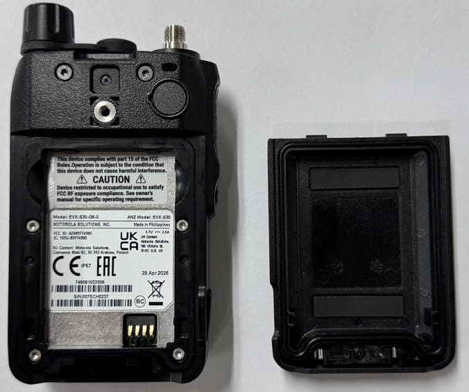
AZ489FT4980
Sep 08, 2026Portable two way radio
Equipment Class
TNF - Licensed Non-Broadcast Transmitter Held to FaceAZ489FT4981
Aug 14, 2026Handheld Portable - TANAPA BPR 45 400-470 MHZ 4W NKP
Equipment Class
TNF - Licensed Non-Broadcast Transmitter Held to Face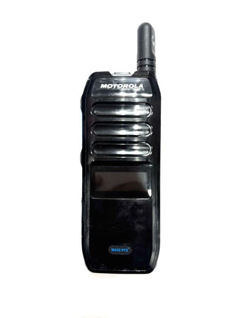
AZ489FT7187
Jul 13, 2026Portable 2-Way Radio with Bluetooth, Bluetooth LE, WIFI 2.4GHz, WIFI 5GHz, LTE
Equipment Class
DSS - Part 15 Spread Spectrum TransmitterAZ499FT6031
May 11, 2026Operation Critical Wireless Earpiece PTT
Equipment Class
DSS - Part 15 Spread Spectrum Transmitter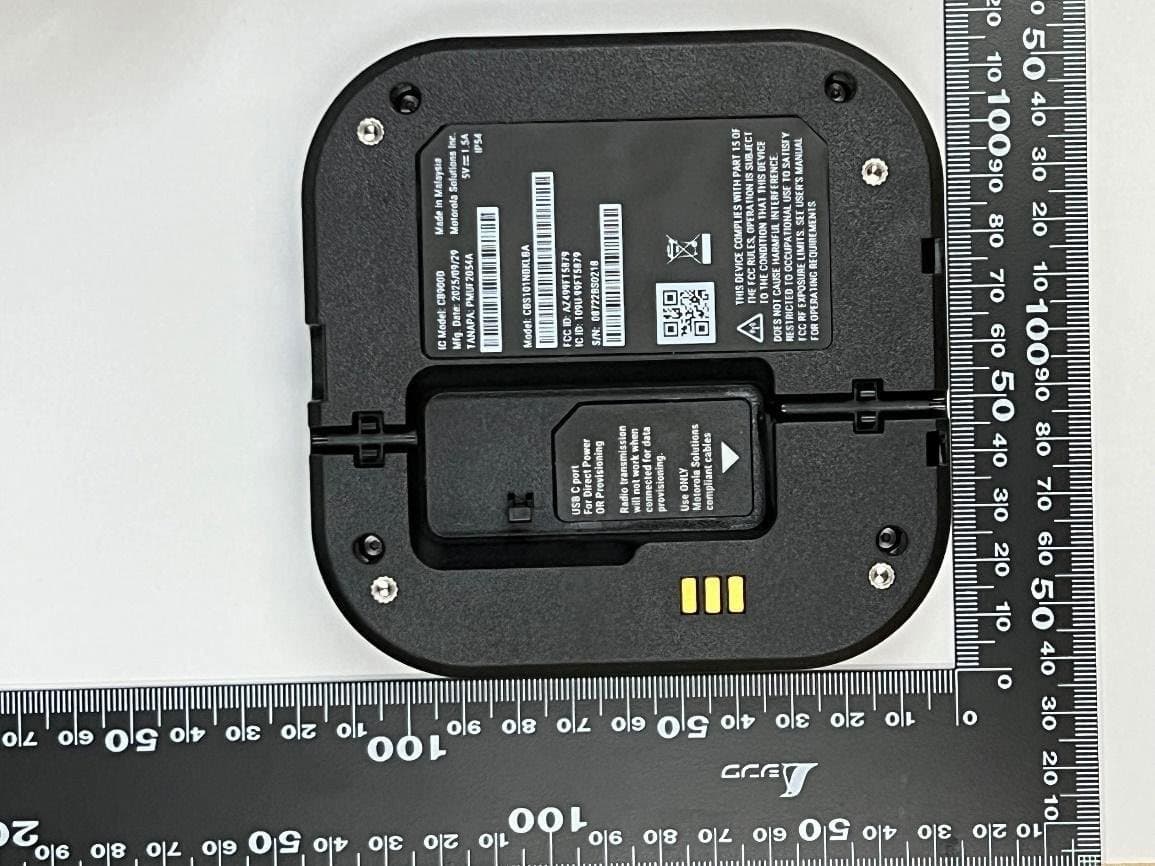
AZ499FT5879
Dec 19, 20252-way Portable Radio with BT, BTLE, WIFI, NFC and LTE
Equipment Class
DSS - Part 15 Spread Spectrum Transmitter