AZ489FT4837Hand Held Transmitter, FM Communication
Motorola Solutions, Inc.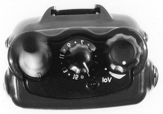
Click to zoom
Application Details
- Equipment Class
- TNF - Licensed Non-Broadcast Transmitter Held to Face
- Date of Grant
- Aug 16, 1999
- Application Purpose
- Original Equipment
- Date of Application
- Jun 07, 1999
- Equipment Note
- Hand Held Transmitter, FM Communication
- Frequency Range
- 403.00000000 - 470.00000000
- Company
- Motorola Solutions, Inc.
- Country
- United States
Documents & Files
Document Text
Text extracted from the exhibit documents filed with the FCC. Open a document above to read the original.
Users Manual
1 English CONTENTS CONTENTS Radio Overview . . . . . . . . . . . . . . . . . . . . 3 Parts of the Radio . . . . . . . . . . . . . . . . . . . 3 On-Off/Volume Knob. . . . . . . . . . . . . . . 4Channel Selector Knob . . . . . . . . . . . . . 4Push-to-Talk (PTT) Button . . . . . . . . . . 4Microphone . . . . . . . . . . . . . . . . . . . . . . 4LED Indicator . . . . . . . . . . . . . . . . . . . . 4Programmable Buttons . . . . . . . . . . . . . 4Menu Keys . . . . . . . . . . . . . . . . . . . . . . 6Keypad Keys . . . . . . . . . . . . . . . . . . . . . 6LCD Screen . . . . . . . . . . . . . . . . . . . . . 6 Indicator Tones . . . . . . . . . . . . . . . . . . . . . 8Programmable Buttons’ Audio Indicators. . 8 Getting Started . . . . . . . . . . . . . . . . . . . . . 9 Battery Information. . . . . . . . . . . . . . . . . . . 9 Charging your Battery . . . . . . . . . . . . . . 9 Accessory Information . . . . . . . . . . . . . . . 10 Attaching the Battery. . . . . . . . . . . . . . 10Removing the Battery . . . . . . . . . . . . . 10Attaching the Antenna. . . . . . . . . . . . . 11Removing the Antenna . . . . . . . . . . . . 11Attaching the Belt Clip. . . . . . . . . . . . . 12Removing the Belt Clip . . . . . . . . . . . . 12 Turning the Radio On or Off . . . . . . . . . . .13Adjusting the Radio’s Volume . . . . . . . . . .13Selecting a Radio Channel . . . . . . . . . . . .13Sending a Call . . . . . . . . . . . . . . . . . . . . . .14Receiving a Call. . . . . . . . . . . . . . . . . . . . .14 Radio Call Information . . . . . . . . . . . . . .15 Repeater or Talkaround Mode. . . . . . . . . .15Setting Tight or Normal Squelch . . . . . . . .15Setting the Power Level. . . . . . . . . . . . . . .16 Scan . . . . . . . . . . . . . . . . . . . . . . . . . . . . .18 Starting or Stopping a Scan Operation . . .18Talkback . . . . . . . . . . . . . . . . . . . . . . . . . .19Deleting a Nuisance Channel . . . . . . . . . .19Adding a Deleted Nuisance Channel back to the Scan List . . . . . . . . . . . . . . . . . . . . . . .19Prioritization of a Scan List member . . . . .19 Phone . . . . . . . . . . . . . . . . . . . . . . . . . . . .21 Making a Phone Call . . . . . . . . . . . . . . . . .21 Entering the Phone Mode. . . . . . . . . . .21Sending the Access Code . . . . . . . . . .21Sending the Phone Number . . . . . . . . .22The Phone Conversation . . . . . . . . . . .23Ending the Phone Call . . . . . . . . . . . . .23 #ELP_Display.book Page 1 Friday, May 14, 1999 5:39 PM 2 English CONTENTS Phone List . . . . . . . . . . . . . . . . . . . . . . . . 24 Adding an Entry to the Phone List . . . 24Deleting an Entry . . . . . . . . . . . . . . . . 24Editing an Entry. . . . . . . . . . . . . . . . . . 25 Audio/Tone Settings . . . . . . . . . . . . . . . 27 General Instructions . . . . . . . . . . . . . . . . . 27 Utilities . . . . . . . . . . . . . . . . . . . . . . . . . . 28 General Instructions . . . . . . . . . . . . . . . . . 28 Safety Information . . . . . . . . . . . . . . . . . 29 Safe And Efficient Operation Of Motorola Two-Way Radios . . . . . . . . . . . . . . . . . . . . . . . 29 Exposure To Radio Frequency Energy 29Portable Radio Operationand EME Exposure . . . . . . . . . . . . . . . 30ElectromagneticInterference/Compatibility . . . . . . . . . . 30Operational Warnings . . . . . . . . . . . . . 30Operational Cautions . . . . . . . . . . . . . 31 Recycling/Disposal of NiCd Batteries. . . . 32 #ELP_Display.book Page 2 Friday, May 14, 1999 5:39 PM RADIO OVERVIEW 3 English RADIO OVERVIEW PARTS OF THE RADIO On-Off/Volume Knob Microphone (programmable) Side Button 1 Push-to-Talk (PTT) Button LED Indicator (programmable) Side Button 2 Channel Selector Knob LCD Screen Menu Keys Keypad Dust Covercovering theAccessoriesPort #ELP_Display.book Page 3 Friday, May 14, 1999 5:39 PM RADIO OVERVIEW 4 English On-Off/Volume Knob Turns the radio on or off, and adjusts the radio’s volume. Channel Selector Knob Switches the radio to different channels. Push-to-Talk (PTT) Button Press and hold down this button to talk; release it to listen. Microphone Speak clearly into the microphone when sending a message. LED Indicator Indicates power-up, radio call and scan status. Programmable Buttons Your radio’s two side buttons can be programmed by your dealer as short-cut buttons for many of the radio’s features.Check with your dealer for a complete list of the functions your radio’s programmable buttons support.The table on page 5 shows the functions available by • short press - quickly pressing and releasing the programmable buttons, or • long press - pressing and holding the programmable buttons for a period of time (at least 1.5 seconds) before releasing, or • hold down - pressing and holding down the programmable buttons while checking status or making adjustments. LED State/Color Indication Radio CallContinuous RedBlinking Red Sending message.Receiving message. Power Level*Continuous Red*Continuous Green Sending message in high power.Sending message in low power. ScanBlinking Green* Scanning for activity. Low BatteryBlinking Red when sending message Low battery level. * Only if this feature is programmed into your radio. Check with your dealer for more details. LED State/Color Indication #ELP_Display.book Page 4 Friday, May 14, 1999 5:39 PM RADIO OVERVIEW 5 English Depending on how your radio has been programmed by your dealer, these functions are activated EITHER through short press OR long press, but NOT both. Button Short Press/Long Press Hold Down Monitor — Monitors the selected channel for any activity. Volume Set — Sounds a tone for adjusting the radio’s volume level. Scan Starts or stops the Scan operation. — Nuisance Channel Delete Deletes a nuisance channel while scanning. — Power Level Toggles your radio’s transmit power level between High and Low power. — Repeater/Talkaround Toggles between using a repeater and transmitting directly to another radio. — Squelch Toggles your radio’s squelch level between tight and norm…
Text truncated - open the document above for the full version.
Attestation Statements
Applicant: Motorola Inc. FCC ID: AZ489FT4837 EXHIBIT 3 STATEMENT OF CERTIFICATION The technical data supplied with this application, having been taken under my supervision is hereby duly certified. The following is a statement of my qualifications: I have received an Electrical & Electronics Engineering degree from The Engineering Council Examination body, United Kingdom, in 1993. I have more than 5 years of Product Development experience in the field of two-way radio communication. NAME: Macwien Krishnamurthi SIGNATURE: Macwien Krishnamurthi DATE: 19th. May. 1999 POSITION: Engineering Group Leader I hereby certify that the above application was prepared under my direction and that to the best of my knowledge and belief, the facts set forth in the application and accompanying technical data are true and correct: NAME: Ng Yong Kian SIGNATURE: YK Ng DATE: 19th.May.1999 POSITION: Engineering Manager
Attestation Statements
Applicant: Motorola Inc FCC ID: AZ489FT4837 EXHIBIT 12 RF EXPOSURE INFORMATION In accordance with 47 CFR 2.1093 (c), this transmitter has been subjected to routine environmental evaluation for RF exposure and found to be compliant with the limits specified in 47 CFR 2.1093 (d).
Block Diagram
Applicant: Motorola Inc. FCC ID: AZ489FT4837 EXHIBIT 5 CIRCUIT DESCRIPTION A general description of the overall circuit is covered in the instruction manual. This section provides the description of circuits required by subpart 2.983 of the Commissions’ Rules. The following are included: 1) Means for Frequency Stabilization 2) Means for Modulation Limiting 3) Means for Attenuation of Higher Audio Frequencies 4) Means for Attenuation of Spurious Emissions 5) Means for Limiting Output Power 6) Means for Modulation Techniques 7) Means for Transient Frequency Behavior Applicant: Motorola Inc. FCC ID: AZ489FT4837 EXHIBIT 5-A 1) Means For Frequency Stabilization Frequency stability is maintained by a reference oscillator/programmable temperature compensation circuit located in the frequency synthesizer IC U201. The oscillator is a Colpitts design with an amplifier in the IC. The 16.8 MHz crystal FL201, varactor and feedback capacitors are external circuitry. A control voltage applied to the varactor via the programmable compensation circuit maintains the frequency stability to within +/-2.5 ppm over temperature. Frequency tuning, also from the programmable compensation circuit, has 128 steps of resolution . Each 16.8 MHz crystal is numerically coded providing its unique characteristic over the temperature range. With the crystal temperature characteristic known, a computed compensation characteristic is programmed into the compensation algorithm. 2) Means for Limiting Modulation Modulation limiting is accomplished within the custom IC, U404. The limiting action itself occurs at the rails (i.e., 3.3V and ground). Using an opamp with feedback, very hard limiting is obtained. The limited modulation signal is then input through a low-pass splatter filter then to an electronic attenuator within U404 in order to adjust for variations in modulation sensitivities of the frequency synthesizer. The electronic attenuator is controlled by the radio’s micro-processor, U409. To keep the deviation constant over the RF frequency range & channel bandwidth, the microcomputer adds the proper correction factor to the attenuator. 3) Means for Attenuation Of Higher Audio Frequencies The output of the limiter is applied to a low-pass splatter filter. This filter is a fifth-order switched capacitor filter with the rolloff corner located at 3000 Hz. The output of the low-pass filter is input to the electronic attenuator before routing to the modulator. 3) Means For Attenuation Of Spurious Emissions The final stage of the RF power amplifier circuit feeds a low-pass filter in order to attenuate harmonics of the carrier frequency as well as any spurious signals. The filter is a Elliptic 7 element design using LC lump elements. 4) Means For Limiting Output Power The radio utilizes a current sense ALC IC U102 to regulate its output power. The current sensing resistor R102 provides a feedback signal to U102. This signal is then compared to the preprogrammed current reference and the error signal is amplified and used to generate a control voltage to control the bias for Driver U101 and final stage RF Power Amplifier, Q110. Applicant: Motorola Inc. FCC ID: AZ489FT4837 EXHIBIT 5-A 6) Means Modulation Techniques The transmitter is capable of the following types of modulation: i) Modulation of PL (Private Line) - Direct FM tone modulation of 67 Hz to 250.3 Hz at 15% of full system deviation. ii) Modulation of DPL (Digital Private Line) - Direct FM modulation at 134 BPS at 15% of full system deviation. iii) Modulation of DTMF tones at nominally 60% of full system deviation Direct FM of PL or DPL is generated by a 6-bit D/A converter contained within U404. The frequency-determining clock signal is generated by the radio microcomputer. The modulation signal is processed through a five pole switched capacitor filter. The output of the filter is input to the electronic attenuator circuit. The microcomputer adjusts the attenuator to compensate for modulation sensitivity variations of the synthesizer & channel bandwidth ensuring 15% of full system deviation for PL and DPL. DTMF tones are generated by the audio processing IC, U404. The tones are routed and processed in the same manner as the voice signals. 7) Means of Transient Frequency Behavior RF power amplifier input impedance swing very wild during sudden turn on. The drastic impedance change can pull or shift the VCO frequency momentarily. This will cause interference to the adjacent channel user. It is very hard to eliminate the problem totally. But FCC has come up a certain requirement on how much power and frequency deviation is allowed to happen during a specific time. This radio is design in such away that the VCO and RF power amplifier are properly isolated. This is achieved by putting a three dB pad in the VCO buffer and the RF PA Pre-driver. Controlling the rate of power rise and down helps significantly in reducing the transients.
Cover Letter(s)
Motorola Inc FCC ID:AZ489FT4837 ______________________________________________________________________________ Radio Products Group 8000 West Sunrise Boulevard, Fort Lauderdale, Florida 33322. (954) 723-5000 Date: June 08, 1999. Authorization & Evaluation Division Federal Communications Commission Laboratory 7435 Oakland Mills Road Columbia, MD 21046 Subject: Application for Certification of Transmitter with FCC ID: AZ489FT4837. Attention: Frank Coperich. Gentlemen: Motorola Inc, 8000 West Sunrise Boulevard, Fort Lauderdale, Florida, herein submits its’ application for Certification of the subject transmitter. This transmitter is primarily intended for use in a portable radio application with capabilities for communications with a transmit power of 1 -- 4.5 Watt. The Power is variable 22% of the value listed (1— 4.5 Watt). The subject transmitter complies with Section 90.203 of the rules in that the operator cannot directly program transmit frequencies using only the unit's normally accessible external controls. Enclosed is a complete Certification application. Contact me at (954) 723-5793 if you require any additional information. Sincerely, Mike Ramnath FCC Liaison Email: [email protected] Fax (954) 723-4794
External Photos
Applicant: Motorola Inc. FCC ID: AZ489FT4837 EXHIBIT 4 EXTERNAL PHOTOGRAPHS This exhibit contains the photographs of this equipment as follows: 1EXHIBIT 4-AFront View (**Plain Model) 2EXHIBIT 4-BFront View (**Display Model) 3EXHIBIT 4-CBack View (**Plain & Display Model) 4EXHIBIT 4-DTop View (**Plain & Display Model) 5EXHIBIT 4-EModel Description NOTE: ** Refer to Exhibit 4-E for model description. Applicant: Motorola Inc. FCC ID: AZ489FT4837 EXHIBIT 4-A Front View (**Plain Model) Applicant: Motorola Inc. FCC ID: AZ489FT4837 EXHIBIT 4-B Front View (**Display Model) Applicant: Motorola Inc. FCC ID: AZ489FT4837 EXHIBIT 4-C Back View (**Plain & Display Model) Applicant: Motorola Inc. FCC ID: AZ489FT4837 EXHIBIT 4-D Top View (**Plain & Display Model) Applicant: Motorola Inc. FCC ID: AZ489FT4837 EXHIBIT 4E MODEL DESCRIPTION Plain Model NumberNameplate AZH34RDC9AA2--GP308 MDH34RDC9AA1--GP040 LAH34RDC9AA1--PRO3150 AAH34RDC9AA1--RP250 AAH34RDC9AA2--RP250 Display Model NumberNameplate AZH34RDH9AA6--- MDH34RDH9AA6--GP080 LAH34RDH9AA6--PRO3150 AAH34RDH9AA6--RP450
ID Label/Location Info
Applicant: Motorola Inc. FCC ID: AZ489FT4837 LIST OF EXHIBITS DESCRIPTIONEXHIBITFCC REFERENCE l.Cover Letter12.1033 llIdentification label information22.983-(f) & General Information2A2.981-(c) & 2.1061 1. Production Plans 2. Application References 3. Data Submittal Procedures IIICertification Of Data32.907 IVExternal Photographs42.983-(g) VBlock Diagrams or Circuit Descriptions52.983-(d)-10,11 1. Frequency Stabilization 2. Modulation Limiting 3. Attenuation Of Higher Audio Frequencies 4. Attenuation Of Spurious Emissions 5. Limiting Output Power 6. Modulation Techniques 7. Transient Frequency Behavior VISchematic Diagrams62.983-(d)-7 VIITest Report7 1. Data Index7 2. RF Output Data7A2.985 (a) 3. Modulation Characteristics2.987 (a) a) Audio Response7B b) Low Pass Filter Response7C c) Modulation Limiting7D 4. Occupied Bandwidth7E2.989 5. Conducted Spurious Emissions7F2.991 6. Radiated Spurious Emissions7G2.993 7. Frequency Stability (Temp. & Supply Volt) 7H & 7I2.995 8. Transient Frequency Behavior 7J2.2.19(EIA/TIA SP-2218) VIIITest Set-Up Procedures8 a) Test Equipment Used b) Method Of Measurements c) Emission Designator Information 1XInstruction Manual9 XInternal Photograph(s)102.983-(g) XIParts List & Tune-Up Procedures11 & 11A2.983-(d)-6 & 2.983-(d)-9 XIIRF Exposure Information12 XIIIOperational Description13 a) Technical Characteristics2.983-(d)-1,2,3,4,5 b) Application Applicant: Motorola Inc. FCC ID: AZ489FT4837 EXHIBIT 2 IDENTIFICATION LABEL LOCATION XSee The Attached Photograph or Sketch Back Of Radio Back Of Radio Under Belt Clip TYPE XThe label is a paper polyester firm laminate with a pressure sensitive adhesive backing. The adhesive is a permanent type acrylic with a minimum peel strength of 40 inches/oz. The label is laser etched into the Urethane paint, exposing the Nickel plating on the Zamak casting substrate. Since no adhesive Is required, the label is permanent and tamper-proof. (**-NOTE- The label attached below is a paper polyester film laminate, as described above. This is just for sample purposes, as the actual label is laser etched into the casting) MARKINGS (TEXT) See the Attached Photograph XLabel Attached Below See Attached Drawing Applicant: Motorola Inc. FCC ID: AZ489FT4837 GENERAL INFORMATION l.Production Plans -- Pursuant 2.981 Quantity production is planned ll.Application References -- Pursuant 2.1061 Reference is made to the following Motorola “Application References” 1. Portable Products and their application 2. Portable Products Transmitter Modulations Methods 3. Motorola Plantation Open Area Test Site lll.Data Submittal Procedure: Data is supplied in accordance with Part 2, Sub-part J of the Commissions’ Rules.
Internal Photos
Applicant: Motorola Inc FCC ID: AZ489FT4837 EXHIBIT 10 INTERNAL PHOTOGRAPHS This exhibit contains, on the following ten pages, photographs of this equipment as follows: 1EXHIBIT 10-BView with The Front Housing open up (**Plain Model) 2EXHIBIT 10-CView with The Front Housing open up (**Display Model) 3EXHIBIT 10-DView with the Back Casting open up (**Plain & Display Model) 4EXHIBIT 10-ETop (Front Housing) Side of RF/Controller Board With Shields Removed (**Plain & Display Model) 5EXHIBIT 10-FBottom (Casting) Side of RF/Controller Board with Shields Removed (**Plain & Display Model) NOTE: ** - Refer to Exhibit 4-E for Model Description Applicant: Motorola Inc FCC ID: AZ489FT4837 EXHIBIT 10-B View With Front Housing Open up (**Plain Model) Applicant: Motorola Inc FCC ID: AZ489FT4837 EXHIBIT 10-C View With Front Housing Open up (**Display Model) Applicant: Motorola Inc FCC ID: AZ489FT4837 EXHIBIT 10-D View With Back Casting Open up (**Plain & Display Model) Applicant: Motorola Inc FCC ID: AZ489FT4837 EXHIBIT 10-E Top (Front Housing) Side Of RF/Controller Board With Shields Removed. (**Plain & Display Model) Applicant: Motorola Inc FCC ID: AZ489FT4837 EXHIBIT 10-F Bottom (Casting) Side Of RF/Controller Board With Sheilds Removed. (**Plain & Display Model)
Operational Description
Applicant: Motorola Inc FCC ID: AZ489FT4837 EXHIBIT 13 OPERATIONAL DESCRIPTION A. Transmitter Technical Characteristics -- Pursuant 2.983 (d) a. RF Power Output:1W to 4.5 Watt Variable Power b. Transmit Frequency Range:403 –470 MHz c. Receive Frequency Range:403 – 470 MHz d. Frequency Stability:2.5 PPM e. Emissions16K0F3E & 11K0F3E (See Exhibit 8-5) f. Spurious Emissions25uW g. DC Voltage and Current into7.5 VDC the final RF amplifier stage/stages1.5 A B. Transmitter Application This transmitter is primarily intended for use in a portable environment. It is characterized by the following features, options, and accessories. a. Power Supply Available: i. NiCd AFAT Battery ii. NiCd Battery iii. NiMH AA Battery iv. NiMH AA FM Battery b. Antenna Available: i. Helical Antenna ii. Whip antenna c. Squelch Type Available: i. Carrier Squelch ii. Tone “Private Line” iii. Digital “Private Line” iv. DTMF v. Quick Call II d. Microphone - Control: i. Handset/Palm Microphone e. Maximum Transmit Channel Capability: i. 16 Channel f. Housing: i. The transmitter will be housed in the housing shown in the accompanying photographs g. Other Options: i. Time out Timer h. The minimum voltage for the micro-Processor to operate is 3.3V.
Parts List/Tune Up Info
Applicant: Motorola Inc FCC ID: AZ489FT4837 EXHIBIT 11 FUNCTION OF RF SEMICONDUCTORS AND OTHER ACTIVE DEVICES SCHEMATICPARTCIRCUITOPERATINGINDUSTRY KEYNUMBERAPPLICATIONFREQUENCYEQUIVALENT CR10148-80973Z02ANTENNA SWITCH403-470 MHzMA4PH261 CR10248-02245J41ANTENNA SWITCH403-470 MHzHSMP3820 CR10551-85963A15POWER AMPLIFIER 403-470 MHz LM50 CR201 48-02233J09SYNTHESIZER16.8 MHz IMN10 CR203 48-62824C03TX VCO FREQ430-470 MHz1SV232 CR24148-05649Q13RX. VCO355-425 MHz1SV228 CR242 & CR24348-62824C01RX. VCO355-425 MHz1SV229 CR25148-02245J22TX. VCO403-470 MHz 1SV229 CR30348-80154K03ESD PROTECTIONDCMMBD353 CR304 & CR30548-62824C01RX. SYSTEM403-470 MHz1SV229 CR30648-02245J42MIXER403-470 MHzHPSM2827 CR30848-02245J41AGCDCHSMP3820 CR31048-62824C012ND OSCILLATOR90.2 MHz1SV229 CR414, CR412 & CR41348-02245J47REVERSE CURRENT DCRB471E PROTECTION CR44048-13833C02REVERSE CURRENTDCMMBD6100 PROTECTION CR50148-80107R01REVERSE CURRENTDCBYD17D PROTECTION CR50348-05729G49LEDDCBRPY1204W D30048-13833C02REVERSE CURRENT DCMMBD6100 PROTECTION Q11048-02245J55POWER AMPLIFIER403-470 MHzPRF1507 Q111,Q210,Q260,Q261 &48-02245J50DC SWITCHDCUMC5N Q417, Q506 Q24148-05218N63VCO OSCILLATOR403-470 MHzBFQ67W Q30148-02245J44RF AMPLIFIER403-470 MHzHP415 Q30248-02245J44IF AMPLIFIER45.1 MHzHP415 Q315,Q505 & Q31648-80214G02DC SWITCHDCMMBT3904 Q32048-05218N632ND OSCILLATOR90.2 MHzBFQ67W Q400 & Q41648-09579E18DC SWITCHDCTP0101T Q40348-80214G02DC SWITCHDCMMBT3904 Q405 & Q41048-02245J54DC SWITCHDCUMG5 Q50258-80159R01DC SWITCHDCLM50 U10151-055109Z67TRANSMITTER SYSTEM403-470 MHzCUSTOM U10251-85765B01TRANSMITTER SYSTEM403-470 MHzCUSTOM U20151-85963A27FGU16.8 MHzCUSTOM U21151-02463J61FGUDCTC7SET04FU U24151-05750U54FGU403-470 MHzCUSTOM U24751-05739X055V VOLTAGE REGULATORDCADP3300 U24851-02463J583.3V VOLTAGE REGULATOR DCLP2980 U30151-09632D83RX. SYSTEMCUSTOM U40051-02463J403.3V VOLTAGE REGULATOR DCAT49BV020 U40451-85963A53AUDIO SYSTEMAUDIOCUSTOM U40651-02463J42CONTROLLER SYSTEM1.83 MHzTK113 U40951-02463J59CONTROLLER SYSTEM1.83 MHzMC74HC4066 U41051-02463J573.3V VOLTAGE REGULATOR DCTDA8547 U42051-02463J44AUDIO AMPLIFIERAUDIOTC7SET04FU VR440-VR444, VR431 &48-02245J51ESD PROTECTION DIODEDCBZX284_6V8 VR506 VR439, VR432, VR43348-80140L15ESD PROTECTION DIODEDCMMBZ5240B VR50148-13830A18ESD PROTECTION DIODEDCMMBZ5235B Q42048-05128M67AMPLIFIERDCMMBT3906 Q602 & Q60348-80214G02DC SWITCHDCMMBT3904 U60251-02463J49KEYPAD BOARDLMC7211 Applicant: Motorola Inc FCC ID: AZ489FT4837 EXHIBIT 11A-1 TUNING PROCEDURES 1. Tuning frequencies These frequencies should be used for transmitter tuning. To avoid interference, the factory should use a frequency offset of 100 kHz from these frequencies for an receiver tuning or testing. Test/Tune FreqVHFUHF Band1 F1136.025403.025 F2142.025413.025 F3148.025425.025 F4154.825437.025 F5161.025449.025 F6167.025460.025 F7173.825469.975 Table 1.0 This procedure was written in the sequence the radio is to be tuned. The following points should be noted: 1) Radio controller refers to the microprocessor in the radio. 2) Tester/test controller refers to external test system (hardware as well as software). 3) Values in tables may change to improve yield. 4) Disable LLE for all tuning and testing. 2. PRO -SCANNING PROGRAMMING 2.1 Flashing 2.2 Download default codeplug 2.3 Scan the 2D barcode of the Reference xtal 2.3.1 Decode of the barcode a)Decode the crystal code to get crystal maximum ppm, crystal inflection temperature (xtal_infl_temp) and crystal curve ppm(t)(crystal ppm at given temperature) and store them in xtal_max_ppm, xtal_infl_temp and xtal_curve_ppm(t). The following equations are used to calculate the above parameters q1=(dig1*10)+dig2 q2=(dig3*100)+(dig4*10)+dig5 q3=(dig6*10)+dig7 xtal_infl_temp=q1/10+22 a1=-q2/1000 a2=(q3+0.1*q2+410)/(5*10^6) delta_temp=temps(t)-ref_temp xtal_curve_ppm(t) =a1*delta_temp+a3*delta_temp^3 where q1: Digits 1 and 2 from xtal code q2: Digits 3,4,5 from xtal code q3: Digits 6 and 7 from xtal code ref_temp: temps(t): Array of temperature in steps of 5 deg c from -35deg C to 90 deg C Applicant: Motorola Inc FCC ID: AZ489FT4837 EXHIBIT 11A-2 2.4 Temperature compensation tuning 2.4.1 Oscillator sensitivity measurement a)Use SBEP command to program synthesizer to receive frequency F7 of table 1.1 and also set the INFLECTION, COLD HOT AND LINEAR dacs to maximum to turn them off (INFLECTION dac= 63 , COLD dac=127, HOT dac=127, LINEAR dac= 63 ) b)Use SBEP command to adjust warp dac to get frequency F7 within +/- 0.2 ppm Store warp dac value in warp_dac_center c)Indicate the PASS/FAIL status of the warp dac value If FAIL: ÏFailed set warp dac valueÓ warp_dac_center must fall within range of 122 to 390 d)Obtain warp_dac_high and warp_dac_low using the equations below: xtal_max_v=(xtal_max_ppm*2)/approx_sens warp_dac_range=ABS(xtal_max_v/warp_dac_step_v) warp_dac_high=INT(warp_dac_center+(warp_dac_range/2)) warp_dac_low=INT(warp_dac_center-(warp_dac_range/2)) where xtal_max_v=maximum required compensation voltage xtal_max_ppm=calculated in 2.3.1a constants: warp_dac_step_v=0.0065 v/step approx_sens=20 ppm/v e)Use SBEP command to program the radio to warp_dac_high f)Use DMM to get voltage reading. Store it in V H g)Use frequency counter to get frequency reading. Store it in F H h)Use SBEP command to program the radio to warp_dac_low i)Use DMM to get voltage reading. Store it in V L j)Use frequency counter to get frequency reading. Store it in F L k)Calculate the oscillator sensitivity using the equation below; comp_range_v=V L -V H ppm_range=[(F L -F H )/F H ]*10^6 osc_sens=ABS(ppm_range/ comp_range_v )+osc_sens_offset where osc_sens=The sensitivity of the oscillatorÌs frequency to the voltage applied to the varactor constants: osc_sens_offset= 0 2.4.2 Translate crystalÌs ppm curve into voltage curve a)Convert the crystal ppm curve vs temperature to voltage vs temperature curve as follows; V(t)=[(xtal_curve-ppm(t)+osc_contrib(t)]/osc_sens where V(t)=voltage at given temperature osc_contrib(t)=determined by hardware tea…
Text truncated - open the document above for the full version.
Schematics
Applicant: Motorola Inc FCC ID: AZ489FT4837 EXHIBIT 6 SCHEMATIC DIAGRAMS The schematic diagrams are as follows: 1Basic Transmitter 2Power Control IC Applicant: Motorola Inc FCC ID: AZ489FT4837 EXHIBIT 6-1 1) BASIC TRANSMITTER Applicant: Motorola Inc FCC ID: AZ489FT4837 EXHIBIT 6-2 2) POWER CONTROL IC
Test Report
Applicant: Motorola Inc FCC ID: AZ489FT4837 EXHIBIT 7 SUBMITTED MEASURED DATA AND METHOD OF MEASUREMENT MEASUREMENTEXHIBITNUMBER OF PAGES IRF Power Output7A 1 IIAudio Response7B 2 IIILow Pass Filter Response7C 2 IVModulation Limiting7D 6 V Occupied Bandwidth7E 12 V1Conducted Spurious Emissions7F12 VIIRadiated Spurious Emissions7G2 VIIIFrequency Stability A. Temperature7H 1 B. Supply Voltage7I 1 IXTransient Frequency Behavior7J4 Applicant: Motorola Inc FCC ID: AZ489FT4837 EXHIBIT 7A RF Power Output - Measured Data The supply voltage to the transmitter was set to 7.5 volts DC. The RF output power was measured with the indicated voltage and current applied into the final RF amplifying device. HIGH - POWER SETTING, FREQUENCY 403.050 MHz. Measured RF Output Power :4.55 WATTS Measured DC Voltage :7.261 VOLTS Measured DC Current :1.43 AMP Measured DC Input Power :10.38 WATTS HIGH - POWER SETTING, FREQUENCY 436.050 MHz. Measured RF Output Power : 4.53 WATTS Measured DC Voltage :7.302 VOLTS Measured DC Current :1.16 AMP Measured DC Input Power :8.47 WATTS HIGH - POWER SETTING, FREQUENCY 469.950 MHz. Measured RF Output Power :4.36 WATTS Measured DC Voltage :7.28 VOLTS Measured DC Current :1.3 AMP Measured DC Input Power :9.46 WATTS LOW - POWER SETTING, FREQUENCY 403.050 MHz. Measured RF Output Power :1.24 WATTS Measured DC Voltage :7.358 VOLTS Measured DC Current :0.84 AMP Measured DC Input Power :6.18 WATTS LOW - POWER SETTING, FREQUENCY 436.050 MHz. Measured RF Output Power :1.31 WATTS Measured DC Voltage :7.367 VOLTS Measured DC Current :0.78 AMP Measured DC Input Power :5.75 WATTS LOW- POWER SETTING, FREQUENCY 469.950 MHz. Measured RF Output Power:1.30 WATTS Measured DC Voltage:7.353 VOLTS Measured DC Current:0.87 AMP Measured DC Input Power: 6.40 WATTS Applicant: Motorola Inc FCC ID: AZ489FT4837 EXHIBIT 7B -1 MOTOROLA INC. TRANSMITTER AUDIO RESPONSE CHARACTERISTIC MODULATION LEVEL vs. AUDIO FREQUENCY =============================================================================== Xmtr Type : AZ489FT4837 Log Page : --- Date : 14th. May 1999 Signature : SF Ooi Frequency: 436.050Mhz Channel Spacing: 25KHz -40.0 -35.0 -30.0 -25.0 -20.0 -15.0 -10.0 -5.0 0.0 5.0 10.0 15.0 100.01000.010000.0100000.0 Audio Frequency in Hz Modulation Level in dB Applicant: Motorola Inc FCC ID: AZ489FT4837 EXHIBIT 7B-2 MOTOROLA INC. TRANSMITTER AUDIO RESPONSE CHARACTERISTIC MODULATION LEVEL vs. AUDIO FREQUENCY =============================================================================== Xmtr Type : AZ489FT4837 Log Page : --- Date : 14th. May 1999 Signature : SF Ooi Frequency: 436.050Mhz Channel Spacing: 12.5KHz -40.0 -35.0 -30.0 -25.0 -20.0 -15.0 -10.0 -5.0 0.0 5.0 10.0 15.0 100.01000.010000.0100000.0 Audio Frequency in Hz Modulation Level in dB Applicant: Motorola Inc FCC ID: AZ489FT4837 EXHIBIT 7C-1 MOTOROLA INC. TRANSMITTER POST - LIMITER ROLL OFF RESPONSE FILTER OUTPUT vs. AUDIO FREQUENCY ================================================================================= Xmtr Type : AZ489FT4837 Log Page : --- Date : 14th. May 1999 Signature : SF Ooi Frequency : 436.050Mhz Channel Spacing : 25KHz -100.00 -80.00 -60.00 -40.00 -20.00 0.00 20.00 100.001000.0010000.00100000.00 Audio Frequency in Hz dB Applicant: Motorola Inc FCC ID: AZ489FT4837 EXHIBIT 7C-2 MOTOROLA INC. TRANSMITTER POST - LIMITER ROLL OFF RESPONSE FILTER OUTPUT vs. AUDIO FREQUENCY ================================================================================= Xmtr Type : AZ489FT4837 Log Page : --- Date : 14th. May 1999 Signature : SF Ooi Frequency : 436.050Mhz Channel Spacing : 12.5KHz -100.00 -80.00 -60.00 -40.00 -20.00 0.00 20.00 100.001000.0010000.00100000.00 Audio Frequency in Hz dB Applicant: Motorola Inc FCC ID: AZ489FT4837 EXHIBIT 7D-1 MOTOROLA INC. CARRIER SQUELCH AUDIO INPUT LEVEL vs. DEVIATION ================================================================================== Xmtr Type : AZ489FT4837 Log Page : --- Date : 14th. May 1999 Signature : SF Ooi Frequency : 436.050Mhz Channel Spacing : 25 KHz 0 500 1000 1500 2000 2500 3000 3500 4000 4500 5000 5500 6000…
Text truncated - open the document above for the full version.
Contact Information
Applicant
Deanna Zakharia(Regulatory Compliance Manager)
Technical Contact
Motorola IncMike Ramnath
[email protected]954-723-5793
8000 West Sunrise Blvd · Ft. Lauderdale, Florida · United States
Non-Technical Contact
MotorolaMike Ramnath
[email protected]954-723-5793
Technical Specifications
| # | Rule Parts | Frequency Range | Power Output | Emission | Tolerance |
|---|---|---|---|---|---|
| 2 | 90.21 | 403 MHz - 470 MHz | 4.5 W | 11K0F3E | 2.5 ppm |
Other Applications from Motorola Solutions, Inc.
AZ489FT4980
Sep 08, 2026Portable two way radio
Equipment Class
TNF - Licensed Non-Broadcast Transmitter Held to FaceAZ489FT4981
Aug 14, 2026Handheld Portable - TANAPA BPR 45 400-470 MHZ 4W NKP
Equipment Class
TNF - Licensed Non-Broadcast Transmitter Held to Face
AZ489FT7187
Jul 13, 2026Portable 2-Way Radio with Bluetooth, Bluetooth LE, WIFI 2.4GHz, WIFI 5GHz, LTE
Equipment Class
DSS - Part 15 Spread Spectrum TransmitterAZ499FT6031
May 11, 2026Operation Critical Wireless Earpiece PTT
Equipment Class
DSS - Part 15 Spread Spectrum Transmitter
AZ499FT5879
Dec 19, 20252-way Portable Radio with BT, BTLE, WIFI, NFC and LTE
Equipment Class
DSS - Part 15 Spread Spectrum Transmitter