AZ489FT5796Data-only integrated transciever
Motorola Solutions, Inc.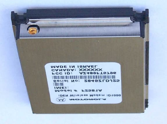
Click to zoom
Application Details
- Equipment Class
- TNB - Licensed Non-Broadcast Station Transmitter
- Date of Grant
- Dec 07, 1999
- Application Purpose
- Original Equipment
- Date of Application
- Aug 19, 1999
- Equipment Note
- Data-only integrated transciever
- Frequency Range
- 806.00000000 - 821.00000000
- Company
- Motorola Solutions, Inc.
- Country
- United States
Documents & Files
Document Text
Text extracted from the exhibit documents filed with the FCC. Open a document above to read the original.
Users Manual
Applicant: Motorola Inc FCC ID: AZ489FT5796 IDEN, Motorola Inc., 8000 Sunrise Blvd., Plantation, FL 33322, USA WWW.MOT.COM/iDEN Page: 8-1 Exhibit 8: No user instruction manual is provided since the modem will be marketed as an Original Equipment Manufacturer (OEM) transceiver module to be embedded in a variety of end products, as described in 47 CFR 2.1091(d)(4). It is supplied neither with battery nor antenna, only with an antenna connector. The characteristics of having an antenna connector and no antenna are like those of transmitters classified as a mobile device, as defined in 47 CFR 2.1091(b), rather than a handheld portable device as defined in 47 CFR 2.1093(b). The type of antenna utilized with this OEM transceiver module, be it interior or exterior to the end product, is not at the discretion of this applicant. Given the 0.7 Watt output power of this transceiver module, and the manufacturer’s discretion for selecting an antenna, it is possible that in use the ERP of this module could exceed the ERP limit in 47 CFR 2.1091(c) for exemption from routine environmental review. Thus, this module was environmentally evaluated for RF Exposure as a mobile device, and was found to be compliant with the MPE General Population limits for a mobile device in Table 1(B) of 47 CFR 2.1310 as required by 47 CFR 2.1091(c). Since the end product may, in some cases, be used within a digital device such as a laptop computer to be marketed in the United States, it is our expectation that the end product may bear a separate FCC identifier in accordance with 47 CFR 2.925(b)(1). It will be the responsibility of the OEM to conduct appropriate RF exposure evaluations, develop user manual information and obtain FCC equipment authorization for the end product manual information needed to gain Authorization. It is our intention to provide the OEM party with a letter notifying them of the need to comply with 47 CFR part 2 subpart J, et. al., once a purchasing agreement has been reached
Attestation Statements
Applicant: Motorola Inc FCC ID: AZ489FT5796 IDEN, Motorola Inc., 8000 Sunrise Blvd., Plantation, FL 33322, USA WWW.MOT.COM/iDEN Page: 2- 1 Exhibit 2. Statement of Certification -----47 CFR. 2.911 The technical data supplied with this application, having been taken under my supervision is hereby duly certified. The following is a statement of my qualifications: B.S. Electrical Engineering, 1988, Tel-Aviv University, Israel M.S. Electrical Engineering, 1995, Tel-Aviv University, Israel 10 years of experience in RF measurement techniques; 5 years of Design and Development experience in the field of two-way radio communication. NAME: Haim Friedlander SIGNATURE: Haim Friedlander DATE: August 19, 1999. POSITION: RF Development Staff Engineer I hereby certify that the above application was prepared under my direction and that to the best of my knowledge and belief, the facts set forth in the application and accompanying technical data are true and correct: NAME: Zami Schwartzman SIGNATURE: Zami Schwartzman DATE:August 19, 1999. POSITION: Engineering Manager
Cover Letter(s)
Applicant: Motorola Inc FCC ID: AZ489FT5796 www.mot.com/iDEN iDEN, Motorola Inc., 8000 W. Sunrise Blvd., Plantation, FL 33324 Page: 13- 1 Date: August 20, 1999 Mr. Frank Coperich Authorization & Evaluation Division Federal Communications Commission Laboratory 7435 Oakland Mills Road Columbia, MD 21046 Dear Mr. Coperich; Motorola Inc., 8000 West Sunrise Boulevard, Fort Lauderdale, Florida 33322, herein submits it’s application for Certification of the subject transmitter. This data-only OEM (Original Equipment Manufacturer)-integrated transceiver uses nearly identical circuitry and software utilized in a previously certified i1000plus hand-held portable transceiver with FCC ID: AZ489FT5793. The circuitry has been repackaged into a module. This module will be marketed to OEMs, who will integrate it into their equipment, i.e. lap-top computers, portable/mobile terminals, vending machines, etc. The Power is variable from 0.0024 Watt to 0.7 Watt, which is 0.3% of the value listed. Enclosed is a complete Certification Application comprised of 13 Exhibits. Contact me at (954) 723-5793 if you require any additional information. Regards, Mike Ramnath FCC Liaison Email: [email protected]
Cover Letter(s)
Applicant: Motorola Inc FCC ID: AZ489FT5796 www.mot.com/iDEN iDEN, Motorola Inc., 8000 W. Sunrise Blvd., Plantation, FL 33324 Page: 13- 1 Date: October 18, 1999 Mr. Frank Coperich Authorization & Evaluation Division Federal Communications Commission Laboratory 7435 Oakland Mills Road Columbia, MD 21046 Dear Mr. Coperich; Motorola Inc., 8000 West Sunrise Boulevard, Fort Lauderdale, Florida 33322, herein submits it’s response to the October 13 request for information on FCC ID: AZ489FT5796, EA95210. We respect the FCC’s recommendations regarding Exhibit 8. However, item 3 of Exhibit 8 is more appropriate and acceptable to Motorola. For the ease of reference, we are attaching item 3 of Exhibit 8. “Since the end product may, in some cases, be used within a digital device such as a laptop computer to be marketed in the United States, it is our expectation that the end product may bear a separate FCC identifier in accordance with 47 CFR 2.925(b)(1). It will be the responsibility of the OEM to conduct appropriate RF exposure evaluations, develop user manual information and obtain FCC equipment authorization for the end product manual information needed to gain Authorization. It is our intention to provide the OEM party with a letter notifying them of the need to comply with 47 CFR part 2 subpart J, et. al., once a purchasing agreement has been reached.” Please contact me at (954) 723-5793 if you require any additional information. Regards, Mike Ramnath FCC Liaison Email: [email protected]
External Photos
Applicant: Motorola Inc FCC ID: AZ489FT5796 IDEN, Motorola Inc., 8000 Sunrise Blvd., Plantation, FL 33322, USA WWW.MOT.COM/iDEN Page: 3- 1 Exhibit 3. External Photographs--------pursuant 47 CFR 2.1033(c)12 Photograph 3-1: Top view of the transceiver Applicant: Motorola Inc FCC ID: AZ489FT5796 IDEN, Motorola Inc., 8000 Sunrise Blvd., Plantation, FL 33322, USA WWW.MOT.COM/iDEN Page: 3- 2 Photograph 3-2: Bottom view of the transceiver Applicant: Motorola Inc FCC ID: AZ489FT5796 IDEN, Motorola Inc., 8000 Sunrise Blvd., Plantation, FL 33322, USA WWW.MOT.COM/iDEN Page: 3- 3 Photograph 3-3: Angled view of transceiver, showing antenna connector
ID Label/Location Info
Applicant: Motorola Inc FCC ID: AZ489FT5796 IDEN, Motorola Inc., 8000 Sunrise Blvd., Plantation, FL 33322, USA WWW.MOT.COM/iDEN Page: 1- 1 Table of Contents EXHIBIT 1. IDENTIFICATION LABEL-----47 CFR. 2.1033 (C)11................................................................................. 1-1 EXHIBIT 1A. GENERAL INFORMATION-----47 CFR. 2.1031, 2.1061............................................................................. 1-2 1A.1. Production Plans -- Pursuant 47 CFR 2.1031............................................................................................................. 1-2 1A.2. Application References -- Pursuant 47 CFR 2.1061.................................................................................................. 1-2 1A.3. Data Submittal Procedure.......................................................................................................................................... 1-2 1A.4. Similar, currently Type Accepted Transmitter........................................................................................................... 1-2 EXHIBIT 2. STATEMENT OF CERTIFICATION-----47 CFR. 2.911............................................................................. 2-1 EXHIBIT 3. EXTERNAL PHOTOGRAPHS---47 CFR. 2.1033(C)12............................................................................... 3-1 EXHIBIT 4. CIRCUIT DESCRIPTION-----47 CFR. 2.1033(C)10.................................................................................... 4-1 4.1. Carrier Frequency Generation and Stabilization........................................................................................................... 4-2 4.2. Digital Modulation Techniques.................................................................................................................................... 4-4 4.3. Modulation Limiting and Post Limiter Filter................................................................................................................ 4-4 4.4. Means for Output Power Limiting................................................................................................................................ 4-5 4.5. Spurious and Harmonic Emissions Suppression............................................................................................................ 4-6 EXHIBIT 5. CIRCUIT DIAGRAMS-----47 CFR. 2.1033(C)10.......................................................................................... 5-1 5.1. Schematic Diagram of Transmitter Block...................................................................................................................... 5-1 6.1. RF Power Output Data -- Pursuant 47 CFR 2.1046(a), 2.1033(c)(6), 2.1033(c)(7) and 2.1033(c)(8)............................. 6-1 6.2. Modulation Characteristics Data -- Pursuant 47 CFR 2.1047 and 2.1033(c)(13)........................................................... 6-1 6.3. Occupied Bandwidth Data -- Pursuant 47 CFR 2.1049, 90.210(g) and 90.691.............................................................. 6-4 6.4. Radiated Spurious Emissions Data -- Pursuant 47 CFR 2.1053,2.1057, 90.210(g) and 90.691(a)................................ 6-18 6.5. Conducted Spurious Emissions Data -- Pursuant 47 CFR 2.1051, 2.1057, 90.210 (g) and 90.691............................... 6-22 6.6. Frequency Stability Data -- Pursuant 47 CFR 2.1055.................................................................................................. 6-23 EXHIBIT 7. MEASUREMENT PROCEDURES.............................................................................................................. 7-1 7.1. RF Power Output -- Pursuant 47 CFR 2.1046............................................................................................................... 7-1 7.2. Occupied Bandwidth -- Pursuant 47 CFR 2.1049.......................................................................................................... 7-1 7.3. Radiated Spurious Emissions -- Pursuant 47 CFR 2.1053............................................................................................. 7-2 7.4. Conducted Spurious Emissions -- Pursuant 47 CFR 2.1051.......................................................................................... 7-3 7.5. Frequency Stability -- Pursuant to 47 CFR 2.1055 and 90.213...................................................................................... 7-3 7.6. Radiated Receiver Spurious Emissions -- Pursuant to 47 CFR 15.107, 15.109................................................................7-5 7.6. Measurement Equipment List ---- 47 CFR 2.1041........................................................................................................ 7-6 EXHIBIT 8. INSTRUCTION MANUAL........................................................................................................................... 8-1 EXHIBIT 9. INTERNAL PHOTOGRAPHS..................................................................................................................... 9-1 EXHIBIT 10. SEMICONDUCTOR/ACTIVE DEVICES LIST AND TUNE UP PROCUDURE...................................... 10-1 10.1. Semiconductor/Active Devices list............................................................................................................................ 10-1 10.2. Tune Up Procedure................................................................................................................................................... 10-2 EXHIBIT 11. RF EXPOSURE INFORMATION............................................................................................................ 11-1 EXHIBIT 12. TRANSMITTER DESCRIPTION-----47 CFR. 2.1033 (C)-4,5,6,7,8......................................................... 12-1 12.1. Transmitter Technical Characteristics...................................................................................................................... 12-1 12.2. Transmitter Application.......................…
Text truncated - open the document above for the full version.
Internal Photos
Applicant: Motorola Inc FCC ID: AZ489FT5796 IDEN, Motorola Inc., 8000 Sunrise Blvd., Plantation, FL 33322, USA WWW.MOT.COM/iDEN Page: 9- 1 Exhibit 9. Internal Photographs: Photograph 9-1: Top side of transceiver RF Board. Photograph 9-2: Bottom side of transceiver RF Board. Applicant: Motorola Inc FCC ID: AZ489FT5796 IDEN, Motorola Inc., 8000 Sunrise Blvd., Plantation, FL 33322, USA WWW.MOT.COM/iDEN Page: 9- 2 Photograph 9-3: Top side of transceiver Logic Board. Photograph 9-4: Bottom side of transceiver Logic Board.
Operational Description
Applicant: Motorola Inc FCC ID: AZ489FT5796 IDEN, Motorola Inc., 8000 Sunrise Blvd., Plantation, FL 33322, USA WWW.MOT.COM/iDEN Page: 12- 1 Exhibit 12. Transmitter Description -----47 CFR. 2.1033 (c) 4,5,6,7,8 12.1.Transmitter Technical Characteristics This trunked radio transceiver is of the receive first type, meaning it must first find, acquire and lock onto a control channel from a predefined set of control frequencies assigned to a compatible base station. Transmission is not possible until acquisition and lock has been achieved, then it is limited to transmission of service request bursts on the digitally modulated reverse control channel. Upon recognition of a proper request, the control channel base station transmitter will then assign the transceiver a traffic channel for transmission of digital circuit switched or packet switched data from the set of frequencies for which the trunking system is licensed. In addition to controlling the assigned frequency to which the transceiver will be slaved, the base station frequency serves as an accurate, stable reference for the transceiver local reference oscillator by virtue of an AFC function inherent in the acquisition and lock process. The base station allocates the number of 15ms time division multiplex (TDM) time slots in which the transceiver transmits, depending on the user requested transmission mode. The trunking system protocol for data transmission uses a 90ms frame divided into six 15 ms time slots. These slot allocations are summarized in Table 12.1 below. Transmission ModeTime Slots Allocated Per FrameDuty Cycle 1:6 Circuit Switched Data Mode116.67% 1:3 Circuit Switched Data Mode233.33% Packet Data Mode up to 81 of 120 slotsup to 67.5% Table 12.1: Time Slot Allocation Table RF Power Output Transmitter output power may be automatically attenuated by up to 24 dB below the maximum transmitter output power setting upon receipt of a command signal from the base station to prevent base station receiver overload. The user has no control over this setting. The nominal mean average power available at the antenna connector for the various transmission modes and for the minimum and maximum power settings are summarized in the Table 12.2 below: Applicant: Motorola Inc FCC ID: AZ489FT5796 IDEN, Motorola Inc., 8000 Sunrise Blvd., Plantation, FL 33322, USA WWW.MOT.COM/iDEN Page: 12- 2 Transmissio n Mode Pulse Average Power at Minimum Power Setting (W) Pulse Average Power at Maximum Power Setting (W) Frame Average Power at Minimum Power Setting (W) Frame Average Power at Maximum Power Setting (W) 1:6 Circuit Switched Data Mode 0.00240.70.00040.1 1:3 Circuit Switched Data Mode 0.00240.70.00080.2 Packet Data Mode 0.00240.70.00162 (over 20 frames) 0.405 (over 20 frames) Table 12.2: RF Power Output A. Pulse Average Output Power Specification0.0024 W---0.7 W Maximum B. Frequency Range806-821 MHz C. Frequency Stability1.9 PPM * D. Emission Designator18K3D7W E. Spurious Emissions< -16 dBm F. DC Voltage and Current into the final RF amplifier stage/stages3.6 Volts DC nominal 240 mA mean current at 1:6 Mode 480 mA mean current at 1:3 Mode 972 mA mean current at Packet Mode * See exhibit 6.6 12.2.Transmitter Application The radio is characterized by the following features, options, and accessories. A. Development/Test Board: A circuit board that provides a flex cable connection to the transceiver and allows connection of DC supply, serial data and access to all other flex cable functions via standard connectors and test points. B. Other Accessories Available: none C. Maximum Transmit Channel Capability All channels in the 806-821 MHz band that is a multiple of 12.5 kHz. This includes EA based SMR service channels. D. Housing The transmitter will be housed in the housing shown in the accompanying photographs. Applicant: Motorola Inc FCC ID: AZ489FT5796 IDEN, Motorola Inc., 8000 Sunrise Blvd., Plantation, FL 33322, USA WWW.MOT.COM/iDEN Page: 12- 3 E. Other Options: none 12.3. Transmitter Programmability The subject transmitter complies with 47 CFR 90.203 in that it is not front panel programmable by the operator. The transmitter internal control computer automatically selects one of the preprogrammed frequency channels in coordination with the trunking systems control channel. The transceivers authorized transmit frequency list is preprogrammed at the factory and can not be changed by the operator. The programming of available transmitter frequency channels by an authorized service person is accomplished by the use of a personal computer using MS-DOS, a Level Shifter card, and licensed “Radio Service Software” (RSS). No operation, receive or transmit is permitted during programming of the portable radio. The transceiver can transmit only after it’s receiver has acquired and locked onto the base station. The maximum frequency error of the transceiver is 1.9 PPM based on the base station meeting the FCC requirement of 1.5 PPM. This locking ensures an accurate transmission frequency. For further description please refer to exhibit 6.6.
Parts List/Tune Up Info
Applicant: Motorola Inc FCC ID: AZ489FT5796 IDEN, Motorola Inc., 8000 Sunrise Blvd., Plantation, FL 33322, USA WWW.MOT.COM/iDEN Page: 10- 1 Exhibit 10. Semiconductor/Active Device List and Tune up Procedure 10.1 Semiconductor/Active Device List SchematicMOTOROLAVENDORDeviceCircuitOperatingSource KEYPART #PART #TypeApplicationFrequency CR301, CR302 4802233J091MN10TRIPLE DIODEDC/DC Converter 1.05 MHz ROHM Q304, Q305,4805793Y01NE68519-T1NPN TRANSISTORMain VCO Buffer 956.90 – 975.6375 MHZ NEC Q6024805793Y01NE68519-T1NPN TRANSISTORTX Offset VCO 301.8 MHz NEC D3004809641F03BB639VARACTOR DIODE Main VCO 956.90 – 975.6375 MHZ TOSHIBA D3014862824C011SV229VARACTOR DIODE Main VCO 956.90 – 975.6375 MHZ TOSHIBA FL0014809995L05CC4V-T1XTAL QUARTZ 32.768KHZ CC Clock Oscillator 32.8 Khz MICROCRYST AL CR5014885908A01MA4P275-1141TPIN DIODEAntenna RX/TX Switch 806-866 MHZ M/A-COM CR5024885908A02MA4P789-1141TPIN DIODEAntenna RX/TX Switch 806-866 MHZ M/A-COM CR6024809877C081SV279VARACTOR DIODE Offset VCO 301.8 MHz TOSHIBA U0045185963A03LM2664M6XDC/DC CONVERTERNegative Volt Inverter 160 KHz National Semi U3015105835U92AT25016-0Z1TSYNTH. ICMain Synthesizer 956.90 – 975.6375 MHZ ATMEL U3025185963A02LM2665M6XDC/DC CONVERTERMain VCO DC Supply 160 KHz National Semi U4015105835U79SC380044VFA/D & D/A IC Modulation A/D, D/A for TX & RX 16.8 MHz MOTOROLA SPS U5015105457W87CUSTOMQUADRATURE MODULATOR & LINEARIZATION IC TX I/Q modulator and RFPA linearity improvement 806-821 MHZ MOTOROLA SPS U5045105385Y78XIM5Y78RF PARF Power Amplifier 806-821 MHZ MOTOROLA SPS U6015105835U76AT25004QUADRATURE RECEIVER IC RX I/Q demodulation, AGC and 2 nd LO/TX offset PLL 219.3-309.6 MHZ ATMEL U8015185130C15CUSTOMCONTROLLER/DSP IC Controller and DSP up to 60 MHZ MOTOROLA SPS COMMENTS: The Motorola designators are special code numbers for active devices used in Motorola radios. These devices are either identical or derived from the device family listed under Source, by the manufacturer or are proprietary to Motorola. Service people do not have access to any cross-references or given any information on proprietary devices and are prevented from making unauthorized substitution. Applicant: Motorola Inc FCC ID: AZ489FT5796 IDEN, Motorola Inc., 8000 Sunrise Blvd., Plantation, FL 33322, USA WWW.MOT.COM/iDEN Page: 10- 2 10.1. Tune Up Procedure ----47 CFR. 2.1033(c)(9) All adjustments are software controlled and pre-set at the factory. The service concept is of field replaceable radio substitution. When a radio is determined to be faulty it is replaced. The faulty radio is then forwarded to a high technology center. There it is repaired and returned to the factory for tuning.
RF Exposure Info
Applicant: Motorola Inc FCC ID: AZ489FT5796 IDEN, Motorola Inc., 8000 Sunrise Blvd., Plantation, FL 33322, USA WWW.MOT.COM/iDEN Page: 11- 1 Exhibit 11: See Exhibit 8 for RF Exposure Statement.
Schematics
Applicant: Motorola Inc FCC ID: AZ489FT5796 IDEN, Motorola Inc., 8000 Sunrise Blvd., Plantation, FL 33322, USA WWW.MOT.COM/iDEN Page: 5- 1 Exhibit 5. Circuit Diagrams-----47 CFR. 2.1033(c)(10) 5.1.Schematic Diagram of Transmitter Block
Test Report
Applicant: Motorola Inc FCC ID: AZ489FT5796 IDEN, Motorola Inc., 8000 Sunrise Blvd., Plantation, FL 33322, USA WWW.MOT.COM/iDEN Page:6-1 Exhibit 6. Measured Data ----- 47 CFR. 2.1033(c)14 6.1.RF Power Output Data -- Pursuant 47 CFR 2.1046(a), 2.1033(c)(6), 2.1033(c)(7) and 2.1033(c)(8) The RF power output was measured with the indicated voltage applied to and current into the final RF amplifying device (U504). The power and current given represents a transmit slot and is not averaged. At the minimum power setting: Measured RF output2.4milliWattsPulse Mean Power Normal DC Voltage3.6Volts Mean DC Current1140 mAPulse Mean Current During Transmit Slot Input Power for the final RF Amplifying Module0.290microWatts At the maximum power setting: Measured RF output0.7WattsPulse Mean Power Normal DC Voltage3.6Volts Mean DC Current1490mAPulse Mean Current During Transmit Slot Input Power for the Final RF Amplifying Module0.1905milliWatts 6.2.Modulation Characteristics Data -- Pursuant 47 CFR 2.1047 and 2.1033(c)(13) Digitally encoded speech or digital data is transmitted in four sub-channels at a 4 kHz rate using M-ary symbols mapped to predetermined fixed magnitude and phase components within 1 of 3 constellations associated with a particular modulation scheme. Figure 6-2 illustrates symbol mapping to one of the four QPSK member constellation. Figure 6-3 illustrates symbol mapping to one of the four 16QAM member constellation. Figure 6-4 illustrates symbol mapping to one of the four 64QAM member constellation. For Quad-QPSK modulation, this mapping adjusts the amplitude and phase variations of the baseband signal to one of 4 points on the constellation. For Quad-16QAM modulation, this mapping adjusts the amplitude and phase variations of the baseband signal to one of 16 points on the constellation. For Quad-64 modulation, this mapping adjusts the amplitude and phase variations of the baseband signal to one of 64 points on the constellation. After conversion by the D/A converters in U401 (see Figure 4-3 in Exhibit 4.3), the necessary bandwidth of the sub-channels is limited to 4.8 kHz by the pair of modulation limiting low pass filters.. The transfer response of these filters is depicted in Figure 6-1where the filter excess bandwidth coefficient of 0.2 is shown. This excess bandwidth leads to the necessary bandwidth calculation of (1 + 0.2) x (4 kHz) = 4.8 kHz. Since the sub-channels are spaced 4.5 kHz apart, the necessary Applicant: Motorola Inc FCC ID: AZ489FT5796 IDEN, Motorola Inc., 8000 Sunrise Blvd., Plantation, FL 33322, USA WWW.MOT.COM/iDEN Page:6-2 bandwidth of the composite 4 sub-channel symbol streams is 4.8 + (3 x 4.5) = 18.3 kHz. 0.707 02k2.4k-2k H(f)=root raised cosine a=0.2 Modulation Low Pass Filter Response WoW where Wo = 2000 and W= (1+a)Wo = 2400Hz 1 for |f| <2Wo-W H(f)= cos 2 (š/4 (|f| + W -2Wo)/(W-Wo)) for 2Wo-W < |f|<W 0 for |f| >W { Figure 6-1: Modulation Low Pass Filter Response x jy +1+3-1 -3 -3 +1 +3 -3 -1 q Symbol Mapping onto One of Four QPSK Constellations QAM baseband output ready for impression onto a particular subcarrier. Data Source QPSK Encoder Interleaver Subchannel Formatter Modem Interface Bit Stream Complex Symbol Stream Figure 6-2: Symbol Mapping onto One of Four QPSK Constellations Applicant: Motorola Inc FCC ID: AZ489FT5796 IDEN, Motorola Inc., 8000 Sunrise Blvd., Plantation, FL 33322, USA WWW.MOT.COM/iDEN Page:6-3 x jy +1+3-1-3 +1 +3 -3 -1 q Symbol Mapping onto One of Four 16-QAM Constellations QAM baseband output ready for impression onto a particular subcarrier. Data Source 16QAM Encoder Real to Complex Combiner Interleaver Modem Interface Bit Stream Complex Symbol Stream Subchannel Formatter Real Symbol Stream e Figure 6-3: Symbol Mapping onto One of Four 16-QAM Constellations x jy +.5 +3.5-.5-3.5 +.5 +3.5 -3.5 -.5 q Symbol Mapping onto One of Four 64-QAM Constellations QAM baseband output ready for impression onto a particular subcarrier. Data Source 16QAM Encoder Real to Complex Combiner Interleaver Modem Interface Bit Stream Complex Symbol Stream Subchannel Formatter Real Symbol Stream 0 1 -2.0 +2.0 .5 + Figure 6-4: Symbol Mapping onto One of Four 64-QAM Constellations Applicant: Motorola Inc FCC ID: AZ489FT5796 IDEN, Motorola Inc., 8000 Sunrise Blvd., Plantation, FL 33322, USA WWW.MOT.COM/iDEN Page:6-4 6.3.Occupied Bandwidth Data -- Pursuant 47 CFR 2.1049, 90.210(g) and 90.691 The method described in paragraph 7.2 was employed with the following conditions: For Quad-QPSK Modulation: 32K Bits Per Second Pseudo-Random Digital Modulation Vertical: 10 dB/div Carrier Reference: 0 dB corresponds to 0.7 watts (+28.45 dBm) mean power for maximum power setting and 2.4 milliwatts (+3.8 dBm) for minimum power setting. For Quad-16QAM Modulation: 64K Bits Per Second Pseudo-Random Digital Modulation Vertical: 10 dB/div Carrier Reference: 0 dB corresponds to 0.7 watts (+28.45 dBm) mean power for maximum power setting and 2.4 milliwatts (+3.8 dBm) for minimum power setting. For Quad-64QAM Modulation: 96K Bits Per Second Pseudo-Random Digital Modulation Vertical: 10 dB/div Carrier Reference: 0 dB corresponds to 0.7 watts (+28.45 dBm) mean power for maximum power setting and 2.4 milliwatts (+3.8 dBm) for minimum power setting. In Figures 6-5 through Figure 6-16, trace 2 (transmitter performance) was measured using a resolution bandwidth of 300 Hz, while trace 1(reference level) was obtained using a resolution bandwidth of 100 kHz. Trace 3 is the applicable emission mask. Measured Data Refer to Figures 6-5 and 6-6 for Quad-QPSK Modulation performance relative to mask 47 CFR 90.210(g). Refer to Figures 6-7 and 6-8 for Quad-16QAM Modulation performance relative to mask 47 CFR 90.210(g). Refer to Figures 6-9 and 6-10 for Quad-64QAM Modulation performance relative to mask 47 CFR 90.210(g). Refer to Figures 6-11 and 6-12 for Quad-QPSK performance relative to mask 47 CFR FCC 90-691(a). Refer to Figures 6-13 and 6-14 for Quad-16QAM performance relative to mask 47 CFR FCC 90-…
Text truncated - open the document above for the full version.
Test Report
Applicant: Motorola Inc FCC ID: AZ489FT5796 IDEN, Motorola Inc., 8000 Sunrise Blvd., Plantation, FL 33322, USA WWW.MOT.COM/iDEN Page:6-12 Figure 6-11: Quad-QPSK Modulation Performance Relative to Mask 47 CFR FCC 90-691(a), Maximum Power Setting: Applicant: Motorola Inc FCC ID: AZ489FT5796 IDEN, Motorola Inc., 8000 Sunrise Blvd., Plantation, FL 33322, USA WWW.MOT.COM/iDEN Page:6-13 Figure 6-12: Quad-QPSK Modulation Performance Relative to Mask 47 CFR FCC 90-691(a), Minimum Power Setting: Applicant: Motorola Inc FCC ID: AZ489FT5796 IDEN, Motorola Inc., 8000 Sunrise Blvd., Plantation, FL 33322, USA WWW.MOT.COM/iDEN Page:6-14 Figure 6-13: Quad-16QAM Modulation Performance Relative to Mask 47 CFR FCC 90-691(a), Maximum Power Setting: Applicant: Motorola Inc FCC ID: AZ489FT5796 IDEN, Motorola Inc., 8000 Sunrise Blvd., Plantation, FL 33322, USA WWW.MOT.COM/iDEN Page:6-15 Figure 6-14: Quad-16QAM Modulation Performance Relative to Mask 47 CFR FCC 90-691(a), Minimum Power Setting: Applicant: Motorola Inc FCC ID: AZ489FT5796 IDEN, Motorola Inc., 8000 Sunrise Blvd., Plantation, FL 33322, USA WWW.MOT.COM/iDEN Page:6-16 Figure 6-15: Quad-64QAM Modulation Performance Relative to Mask 47 CFR FCC 90-691(a), Maximum Power Setting: Applicant: Motorola Inc FCC ID: AZ489FT5796 IDEN, Motorola Inc., 8000 Sunrise Blvd., Plantation, FL 33322, USA WWW.MOT.COM/iDEN Page:6-17 Figure 6-16: Quad-64QAM Modulation Performance Relative to Mask 47 CFR FCC 90-691(a), Minimum Power Setting: Applicant: Motorola Inc FCC ID: AZ489FT5796 IDEN, Motorola Inc., 8000 Sunrise Blvd., Plantation, FL 33322, USA WWW.MOT.COM/iDEN Page:6-18 6.4.Radiated Spurious Emissions Data -- Pursuant 47 CFR 2.1053, 2.1057, 90.210(g) and 90.691(a). FCC Limits Radiated spurious emissions shall be attenuated below the maximum level of emission of the carrier frequency in accordance with the following formula: Spurious attenuation (dB) = 43 + 10 log 10 (P), P = Power output in watts (0.7 watts in this case). Applicant: Motorola Inc FCC ID: AZ489FT5796 IDEN, Motorola Inc., 8000 Sunrise Blvd., Plantation, FL 33322, USA WWW.MOT.COM/iDEN Page:6-19 Fig. 6-17: Radiated Transmitter Emissions, Tx frequency 813.5625 MHz, Maximum Power, and Horizontally Polarized Antenna. Table 6-1: Radiated Transmitter Emissions, Tx frequency 813.5625 MHz, Maximum Power, and Horizontally Polarized Antenna. TitleFrequency (MHz) FCC Maximum Emission Limit (dBm) Measured Emission Equivalent Power Into an Ideal Dipole (dBm) IF150.9000-13<-40 2X IF301.8000-13<-40 LO964.4625-13<-40 IF + LO1115.3625-13<-40 2X FUND1627.1250-13<-40 3X FUND2440.6875-13<-40 4X FUND3254.2500-13-36.45 5X FUND4067.8125-13<-40 6X FUND4881.3750-13<-40 7X FUND5694.9375-13<-40 8X FUND6508.5000-13 * 9X FUND7322.0625-13 * 10XFUND8135.6250-13 * Note: Measured noise floor (-93 dBm), limited by test setup and equipment. -40 -30 -20 -10 0 150.9000301.8000964.4625 1115.36251627.12502440.68753…
Text truncated - open the document above for the full version.
Contact Information
Applicant
Deanna Zakharia(Regulatory Compliance Manager)
Technical Contact
Motorola IncMike Ramnath
[email protected]954-723-5793
8000 West Sunrise Blvd · Ft. Lauderdale, Florida · United States
Non-Technical Contact
Motorola IncMike Ramnath
[email protected]954-723-5793
Technical Specifications
| # | Rule Parts | Frequency Range | Power Output | Emission | Tolerance |
|---|---|---|---|---|---|
| 1 | 90 | 806 MHz - 821 MHz | 700.00 mW | 18K3D7W | 1.9000000000 ppm |
Other Applications from Motorola Solutions, Inc.
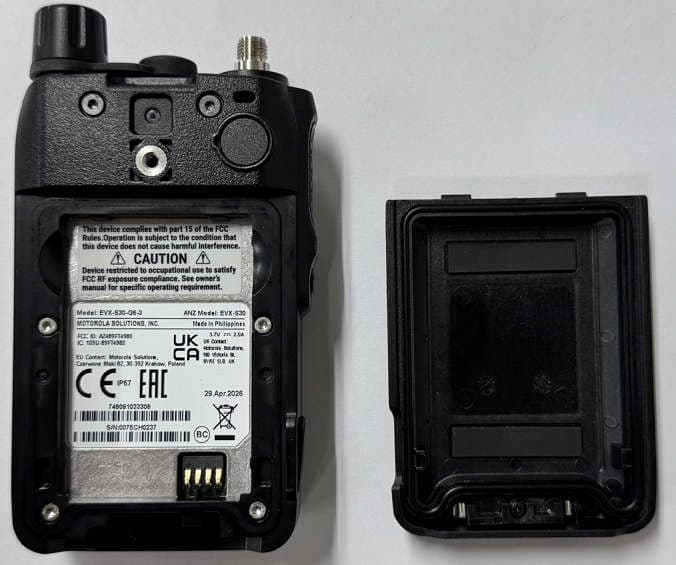
AZ489FT4980
Sep 08, 2026Portable two way radio
Equipment Class
TNF - Licensed Non-Broadcast Transmitter Held to FaceAZ489FT4981
Aug 14, 2026Handheld Portable - TANAPA BPR 45 400-470 MHZ 4W NKP
Equipment Class
TNF - Licensed Non-Broadcast Transmitter Held to Face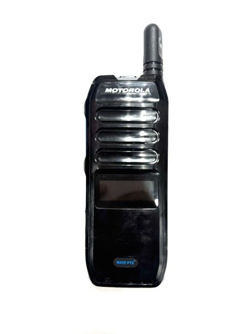
AZ489FT7187
Jul 13, 2026Portable 2-Way Radio with Bluetooth, Bluetooth LE, WIFI 2.4GHz, WIFI 5GHz, LTE
Equipment Class
DSS - Part 15 Spread Spectrum TransmitterAZ499FT6031
May 11, 2026Operation Critical Wireless Earpiece PTT
Equipment Class
DSS - Part 15 Spread Spectrum Transmitter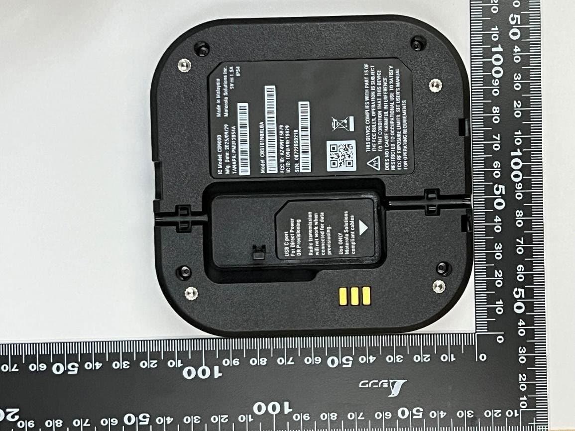
AZ499FT5879
Dec 19, 20252-way Portable Radio with BT, BTLE, WIFI, NFC and LTE
Equipment Class
DSS - Part 15 Spread Spectrum Transmitter