AZ489FT5797iM1000 Wireless Data Modem
Motorola Solutions, Inc.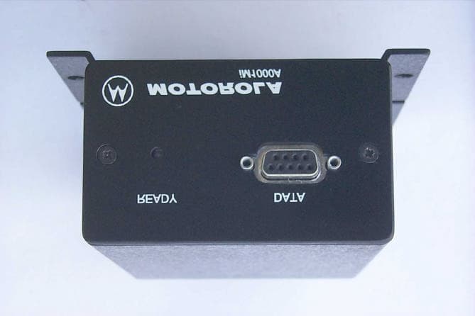
Click to zoom
Application Details
- Equipment Class
- TNB - Licensed Non-Broadcast Station Transmitter
- Date of Grant
- Jan 02, 2000
- Application Purpose
- Original Equipment
- Date of Application
- Aug 17, 1999
- Equipment Note
- iM1000 Wireless Data Modem
- Frequency Range
- 806.00000000 - 821.00000000
- Company
- Motorola Solutions, Inc.
- Country
- United States
Documents & Files
Document Text
Text extracted from the exhibit documents filed with the FCC. Open a document above to read the original.
Attestation Statements
Applicant: Motorola Inc FCC ID: AZ489FT5797 IDEN, Motorola Inc., 8000 Sunrise Blvd., Plantation, FL 33322, USA WWW.MOT.COM/iDEN Page: 2- 1 Exhibit 2. Statement of Certification -----47 CFR 2.911 The technical data supplied with this application, having been taken under my supervision is hereby duly certified. The following is a statement of my qualifications: B.S. Electrical Engineering, 1988, Tel-Aviv University, Israel M.S. Electrical Engineering, 1995, Tel-Aviv University, Israel 10 years of experience in RF measurement techniques; 5 years of Design and Development experience in the field of two-way radio communication. NAME: Haim Friedlander SIGNATURE: Haim Friedlander DATE:_August 18, 1999 POSITION: RF Development Staff Engineer I hereby certify that the above application was prepared under my direction and that to the best of my knowledge and belief, the facts set forth in the application and accompanying technical data are true and correct: NAME: Zami Schwartzman SIGNATURE: Zami Schwartzman DATE: August 18, 1999 POSITION: Engineering Manager
Block Diagram
Applicant: Motorola Inc FCC ID: AZ489FT5797 IDEN, Motorola Inc., 8000 Sunrise Blvd., Plantation, FL 33322, USA WWW.MOT.COM/iDEN Page: 4- 1 Exhibit 4. Circuit Description ----- 47 CFR. 2.1033(c)(10) This section provides the description of circuits required by 47 CFR 2.1033(c)(10). The following are included: 4.1) Carrier Frequency Generation and Stabilization 4.2) Digital Modulation Technique 4.3) Modulation Limiting and Post Limiter Filter 4.4) Means for Output Power Limiting 4.5) Spurious and Harmonic Emissions Suppression Applicant: Motorola Inc FCC ID: AZ489FT5797 IDEN, Motorola Inc., 8000 Sunrise Blvd., Plantation, FL 33322, USA WWW.MOT.COM/iDEN Page: 4- 2 4.1.Carrier Frequency Generation and Stabilization The synthesizer reference oscillator employs a crystal controlled Colpitts oscillator running at a frequency of 16.8Mhz. The oscillator transistor, start-up circuit, and temperature compensation circuit are located in the U301 while the oscillator feedback capacitors, crystal, and tuning varactor are external. This oscillator is temperature compensated to an accuracy of +/-2.5PPM from -25 to 60 degrees C. The method of temperature compensation is to apply an inverse Bechmann voltage curve which matches the crystal's Bechmann curve to a varactor which constantly shifts the oscillator back on frequency. The crystal vendor characterizes the crystal over a specified temperature range and codes this information into an eight-digit code which is printed on the crystal package in a bar code. In production this crystal code is read via a 3-dimensional bar code reader into a custom temperature compensation tuning algorithm. This tuning algorithm decodes the crystal information and takes voltage and temperature measurements on the oscillator then programs U301’s temperature compensation registers to provide the specified frequency error vs. temperature performance. Y300 U301 AFC & TEMP ADJ. Figure 4-1: 16.8 MHz Reference Oscillator The reference oscillator runs at 16.8 MHz. The signal from this reference oscillator Applicant: Motorola Inc FCC ID: AZ489FT5797 IDEN, Motorola Inc., 8000 Sunrise Blvd., Plantation, FL 33322, USA WWW.MOT.COM/iDEN Page: 4- 3 is routed to the synthesizer IC (U301) and is used to control the stability of the main Voltage Controlled Oscillator (VCO) which oscillates at a frequency between 956.9- 971.9 MHz (see figure 4-2). The synthesizer also buffers the 16.8 MHz signal and provides it as a clock signal to U401 (A/D and D/A IC), U501 (TX Quadrature Modulation and Linearization IC), U601 (Quadrature Receiver IC), U001 (DC Power and Audio IC) and U801 (Controller and DSP IC). The PLL inside the U601 uses the 16.8 MHz clock as the reference for the TX Offset VCO and RX 2nd LO VCO. The frequency of the TX Offset VCO is 301.8 MHz which is divided by two in U501 and mixed with the main VCO to generate the transmit frequency. The frequency of the RX 2nd LO VCO is 219.3 MHz which is divided by two in U601 and mixed with the received Intermediate Frequency (IF) signal to generate the baseband data for the DSP. The frequency control for each VCO is accomplished by a PLL inside U601 which compares the VCO frequency (after a frequency divider) to the reference frequency thus phase-locking each VCO to the reference oscillator. The transmitter frequency is programmed to a single frequency between 806-821 MHz composed by subtracting half of the TX offset VCO frequency (301.8 MHz) from the main VCO frequency 956.9-971.9 MHz. The subtraction is done by a mixer in U501, followed by a band pass filter (FL501) which selects the transmitter frequency of 806 - 821 MHz from the other mixing products and rejects spurious signals. ∏8 Clock Generation 16.8MHz 16.8MHz SYNTHESIZER IC 956.9-971.9 MHz Transceiver Frequency Generation Subsystem Main VCO 956.9-971.9 MHz 16.8MHz Reference Oscillator 16.8MHz ∏8 ∏ 1 150.9 MHz 806-821 MHz SYNTHESIZER Phase-Detector and Filter ∏ 2 109.65 Mhz U301 U501 U601 ∏ 2 TX Offset VCO 301.8 MHz RX 2 nd VCO 219.3 MHz Figure 4-2 : Transceiver Frequency Generation Subsystem 4.2.Digital Modulation Techniques Applicant: Motorola Inc FCC ID: AZ489FT5797 IDEN, Motorola Inc., 8000 Sunrise Blvd., Plantation, FL 33322, USA WWW.MOT.COM/iDEN Page: 4- 4 The subject radio makes use of 3 different modulation techniques termed Quad- 16QAM, Quad-64QAM, and Quad-QPSK. In voice mode, the radio will function in Quad-16QAM mode only. In data mode, the radio will use any one of the three different modulation techniques (Quad-16QAM, Quad-64QAM, and Quad-QPSK) in a given slot. The following describes each of the modulation techniques: The modulation technique termed Quad-QPSK is a linear digital modulation of a multi-channel variant of Quadrature Phase Shift Keying (QPSK). Data bits to be transmitted are split into four parallel lower rate streams, each of which is QPSK modulated to its own sub carrier frequency. The four resulting sub channel signals are then combined in frequency division multiplex fashion to produce the composite M-QPSK signal. This spectrally efficient linear modulation can achieve transmission at 32K Bits per Second in a 25 kHz channel. The transmitter is configured using TDMA time slotting so that up to 6 radio users can simultaneously share the 25 kHz channel. The modulation technique termed Quad-16QAM is a linear digital modulation of a multi-channel variant of a 16-state Quadrature Amplitude Modulation. Data bits to be transmitted are split into four parallel lower rate streams, each of which is 16QAM modulated to its own sub carrier frequency. The four resulting sub channel signals are then combined in frequency division multiplex fashion to produce the composite M-16QAM signal. This spectrally efficient linear modulation can achieve transmission at 64K Bits per Second in a 25 kHz channel. The transmitter is configured using TDMA time slotting so that up to 6 radio users can simultaneously share the 25 kHz channel. The modulation technique termed Quad-64QAM is…
Text truncated - open the document above for the full version.
Cover Letter(s)
Applicant: Motorola Inc FCC ID: AZ489FT5797 www.mot.com/iDEN iDEN, Motorola Inc., 8000 W. Sunrise Blvd., Plantation, FL 33324 Page: 13- 1 Date: August 18, 1999 Mr. Frank Coperich Authorization & Evaluation Division Federal Communications Commission Laboratory 7435 Oakland Mills Road Columbia, MD 21046 Dear Mr. Coperich; Motorola Inc., 8000 West Sunrise Boulevard, Fort Lauderdale, Florida 33322, herein submits it’s application for Certification of the subject transmitter. This data only mobile transceiver uses nearly identical circuitry and software utilized in a previously certified i1000plus hand-held portable transceiver with FCC ID: AZ489FT5793. The circuitry has been repackaged into a module which is then installed in a housing intended for Vehicular installations. The Power is variable from 0.0024 Watt to 0.7 Watt, which is 0.3% of the value listed. Enclosed is a complete Certification Application comprised of 13 Exhibits. Contact me at (954) 723-5793 if you require any additional information. Regards, Mike Ramnath FCC Liaison Email: [email protected]
Cover Letter(s)
Applicant: Motorola Inc FCC ID: AZ489FT5797 www.mot.com/iDEN iDEN, Motorola Inc., 8000 W. Sunrise Blvd., Plantation, FL 33322 Date: October 26, 1999 Mr. Frank Coperich Authorization & Evaluation Division Federal Communications Commission Laboratory 7435 Oakland Mills Road Columbia, MD 21046 Dear Mr. Coperich; Motorola Inc., 8000 West Sunrise Boulevard, Fort Lauderdale, Florida 33322, herein submits it’s response to the October 13 request for information on FCC ID: AZ489FT5797, EA95186. 1)This will serve to confirm the intended use of the modem is in vehicles with an external antenna connected to the output jack and mounted to the automobile with an antenna to human separation distance of greater than 20 cm consistent with the definition of a mobile device given in 47 CFR 2.1091(b). No antenna is provided with the modem, so a user must obtain the antenna separately. Three (3) dB gain (relative to a quarter wave whip, 2 dB relative to the dipole reference used for ERP considerations) antenna accessories are provided by Motorola, but other commercially available antennas may be used instead, including some with higher gain or lower loss cables. 2)For categorical exclusion of a 0.7 watt 800 MHz band radio per 47 CFR 2.1091© the antenna gain must not exceed 3.3 dBd (or equivalently, 4.3 dBq) including cable loss. None of the Motorola antenna accessories cited exceed this value, so the product and all 3 associated accessory antennas being offered qualify for categorical exclusion. Antenna cable loss for the Motorola antennas also serve to reduce antenna system gain another 1.5 to 2 dB and is not considered in the gain rating. This cable loss may differ with antenna accessories from other commercial vendors so an antenna with sufficient gain and low cable loss might not qualify for categorical exclusion. Attached per your request is MPE evaluation data obtained in several mounting positions at a separation distance of 20 cm for the 3 categorically excluded Motorola, Inc. antenna accessories cited. The maximum power density measured, as stated in paragraph 3.0, was 0.021 mW/cm 2 . This is about 3.9% of the general population Maximum Permitted Exposure (MPE) limit specified in table 1B in 47 CFR 1.1310. We trust this adequately provides the information you requested. Please contact me at (954) 723-5793 if you require any additional information. Applicant: Motorola Inc FCC ID: AZ489FT5797 www.mot.com/iDEN iDEN, Motorola Inc., 8000 W. Sunrise Blvd., Plantation, FL 33322 Sincerely, Mike Ramnath FCC Liaison Email: [email protected]
Cover Letter(s)
Applicant: Motorola Inc FCC ID: AZ489FT5797 www.mot.com/iDEN iDEN, Motorola Inc., 8000 W. Sunrise Blvd., Plantation, FL 33322 Date: October 26, 1999 Mr. Frank Coperich Authorization & Evaluation Division Federal Communications Commission Laboratory 7435 Oakland Mills Road Columbia, MD 21046 Dear Mr. Coperich; Motorola Inc., 8000 West Sunrise Boulevard, Fort Lauderdale, Florida 33322, herein submits it’s response to the October 13 request for information on FCC ID: AZ489FT5797, EA95186. 1)This will serve to confirm the intended use of the modem is in vehicles with an external antenna connected to the output jack and mounted to the automobile with an antenna to human separation distance of greater than 20 cm consistent with the definition of a mobile device given in 47 CFR 2.1091(b). No antenna is provided with the modem, so a user must obtain the antenna separately. Three (3) dB gain (relative to a quarter wave whip, 2 dB relative to the dipole reference used for ERP considerations) antenna accessories are provided by Motorola, but other commercially available antennas may be used instead, including some with higher gain or lower loss cables. 2)For categorical exclusion of a 0.7 watt 800 MHz band radio per 47 CFR 2.1091© the antenna gain must not exceed 3.3 dBd (or equivalently, 4.3 dBq) including cable loss. None of the Motorola antenna accessories cited exceed this value, so the product and all 3 associated accessory antennas being offered qualify for categorical exclusion. Antenna cable loss for the Motorola antennas also serve to reduce antenna system gain another 1.5 to 2 dB and is not considered in the gain rating. This cable loss may differ with antenna accessories from other commercial vendors so an antenna with sufficient gain and low cable loss might not qualify for categorical exclusion. Attached per your request is MPE evaluation data obtained in several mounting positions at a separation distance of 20 cm for the 3 categorically excluded Motorola, Inc. antenna accessories cited. The maximum power density measured, as stated in paragraph 3.0, was 0.021 mW/cm 2 . This is about 3.9% of the general population Maximum Permitted Exposure (MPE) limit specified in table 1B in 47 CFR 1.1310. We trust this adequately provides the information you requested. Please contact me at (954) 723-5793 if you require any additional information. Applicant: Motorola Inc FCC ID: AZ489FT5797 www.mot.com/iDEN iDEN, Motorola Inc., 8000 W. Sunrise Blvd., Plantation, FL 33322 Sincerely, Mike Ramnath FCC Liaison Email: [email protected]
Cover Letter(s)
FCC ID: AZ489FT5797 www.mot.com/iDEN iDEN, Motorola Inc., 8000 W. Sunrise Blvd., Plantation, FL 33322 Date: December 17, 1999 Mr. Frank Coperich Authorization & Evaluation Division Federal Communications Commission Laboratory 7435 Oakland Mills Road Columbia, MD 21046 Dear Mr. Coperich; Motorola Inc., 8000 West Sunrise Boulevard, Fort Lauderdale, Florida 33322, herein submits it’s response to the December 17 request for information on FCC ID: AZ489FT5797, EA95186 via correspondence number 11076. 1) This device is a “data only Mobile Transceiver”, as noted in Exhibit 13-1 cover letter. Thus, we do not require the D7E emission designator for QAM voice mode, as recommended by the Commission. 2) We accept that the FCC’s recommendation that the 4-QPSK data mode is covered by DXW. Please amend the form 731 and the application to reflect Emission Designator 18K3DXW. 3) In the data mode the radio subchannels may use 16-QAM or 64-QAM modulation as alternatives to 4-QPSK as clarified in Exhibit 6.2 which accompanied our application. Given the use of D as the first symbol for the class of emission, and since the modulation filter is the same for all three modulation methods, we trust that 18K3DXW would be applicable to those as well. 4) The necessary bandwidth calculation was included in Exhibit 6.2 which accompanied our application. We are listing it below for reference. “... the necessary bandwidth of these subchannels is limited to 4.8 kHz by the pair of modulation low pass filters. The transfer response of these filters is depicted in Figure 6-1 where the filter excess bandwidth coefficient of 0.2 is shown. This excess bandwidth leads to the necessary bandwidth calculation of (1 + 0.2) x (4 kHz) = 4.8 kHz. Since the sub-channels are spaced 4.5 kHz apart, the necessary bandwidth of the composite 4 sub-channel symbol streams is 4.8 + (3 x 4.5) = 18.3 kHz.” We trust this adequately provides the information you requested. Please contact me at (954) 723- 5793 if you require any additional information. Sincerely, Mike Ramnath FCC ID: AZ489FT5797 www.mot.com/iDEN iDEN, Motorola Inc., 8000 W. Sunrise Blvd., Plantation, FL 33322 FCC Liaison Email: [email protected]
Cover Letter(s)
FCC ID: AZ489FT5797 www.mot.com/iDEN iDEN, Motorola Inc., 8000 W. Sunrise Blvd., Plantation, FL 33322 Date: December 20, 1999 Mr. Frank Coperich Authorization & Evaluation Division Federal Communications Commission Laboratory 7435 Oakland Mills Road Columbia, MD 21046 Dear Mr. Coperich; Motorola Inc., 8000 West Sunrise Boulevard, Fort Lauderdale, Florida 33322, herein submits it’s response to the December 20 request for information on FCC ID: AZ489FT5797, EA95186, correspondence number 11101. 1) Page 6 of the Antenna Mounting section in the latest revision of the User’s Manual (attached) will be amended and will read as follows: Antenna Mounting “The best mounting location for the antenna is in the center of a large, flat conductive surface. In almost all vehicles, these requirements are best satisfied by mounting the antenna at the center of the roof. Some vehicles have a large trunk lid that provides a good antenna location. If the trunk lid is used, connect grounding straps between the trunk lid and vehicle chassis to ensure the trunk lid is at chassis ground. Three types of antennas can be used: 1. RAFU136A - Magnetic Antenna 2. FAD5524A - Mobile Window Antenna 3. HAF9067A - Mobile Roof Mount Antenna Antennas with gain exceeding 3 dBd do not comply with FCC RF exposure regulations and are not allowed for use with this product. Make sure that you refer to the antenna installation instructions according to the kit number”. Also, page 96 of the User’s Manual for Antenna and Installation Considerations, is listed below for your reference: Antenna and Installation Considerations “ All equipment must be properly installed in accordance with Motorola installation instructions. To assure compliance with United States FCC regulations on RF exposure, the user of the equipment must position the antenna in such a way to maintain a separation of at least 8 inches (20 cms) between the antenna and the body of any user and nearby person. Ensure that the antenna is properly installed external to the vehicle FCC ID: AZ489FT5797 www.mot.com/iDEN iDEN, Motorola Inc., 8000 W. Sunrise Blvd., Plantation, FL 33322 and in accordance with the requirements of the antenna manufacturer/supplier. Use only the supplied or an approved antenna. Unauthorized antennas, modifications, or attachments could impair call quality, damage the modem, or result in violation of the ICNRP or the FCC”. 2)We are in agreement with the Commission’s proposed grant condition that “Antennas for this device must be vehicle mounted to provide at least 20 cm separation between the antenna and persons for satisfying MPE requirements. MPE tested with 3 dBd antennas, use of other antennas must not exceed total system output of 1.5 W ERP. The appropriate information for satisfying RF exposure compliance must be provide to installers and end users”. We trust this adequately provides the information you requested. Please contact me at (954) 723-5793 if you require any additional information. Sincerely, Mike Ramnath FCC Liaison Email: [email protected]
External Photos
Applicant: Motorola Inc FCC ID: AZ489FT5797 IDEN, Motorola Inc., 8000 Sunrise Blvd., Plantation, FL 33322, USA WWW.MOT.COM/iDEN Page: 3- 1 Exhibit 3. External Photographs--------pursuant 47 CFR 2.1033(c)12 Photograph 3-1: Modem front panel Applicant: Motorola Inc FCC ID: AZ489FT5797 IDEN, Motorola Inc., 8000 Sunrise Blvd., Plantation, FL 33322, USA WWW.MOT.COM/iDEN Page: 3- 2 Photograph 3-2: Modem rear panel, showing FCC label.
ID Label/Location Info
Applicant: Motorola Inc FCC ID: AZ489FT5797 IDEN, Motorola Inc., 8000 Sunrise Blvd., Plantation, FL 33322, USA WWW.MOT.COM/iDEN Page: 1- 1 Table of Contents EXHIBIT 1. IDENTIFICATION LABEL-----47 CFR. 2.1033 (C)11................................................................................. 1-1 EXHIBIT 1A. GENERAL INFORMATION-----47 CFR. 2.1031, 2.1061............................................................................. 1-2 1A.1. Production Plans -- Pursuant 47 CFR 2.1031............................................................................................................. 1-2 1A.2. Application References -- Pursuant 47 CFR 2.1061.................................................................................................. 1-2 1A.3. Data Submittal Procedure.......................................................................................................................................... 1-2 1A.4. Similar, currently Type Accepted Transmitter........................................................................................................... 1-2 EXHIBIT 2. STATEMENT OF CERTIFICATION-----47 CFR. 2.911............................................................................. 2-1 EXHIBIT 3. EXTERNAL PHOTOGRAPHS---47 CFR. 2.1033(C)12............................................................................... 3-1 EXHIBIT 4. CIRCUIT DESCRIPTION-----47 CFR. 2.1033(C)10.................................................................................... 4-1 4.1. Carrier Frequency Generation and Stabilization........................................................................................................... 4-2 4.2. Digital Modulation Techniques.................................................................................................................................... 4-4 4.3. Modulation Limiting and Post Limiter Filter................................................................................................................ 4-4 4.4. Means for Output Power Limiting................................................................................................................................ 4-5 4.5. Spurious and Harmonic Emissions Suppression............................................................................................................ 4-6 EXHIBIT 5. CIRCUIT DIAGRAMS-----47 CFR. 2.1033(C)10.......................................................................................... 5-1 5.1. Schematic Diagram of Transmitter Block...................................................................................................................... 5-1 EXHIBIT 6. MEASURED DATA-----47 CFR. 2.1033(C)14............................................................................................... 6-1 6.1. RF Power Output Data -- Pursuant 47 CFR 2.1046(a), 2.1033(c)(6), 2.1033(c)(7) and 2.1033(c)(8)............................. 6-1 6.2. Modulation Characteristics Data -- Pursuant 47 CFR 2.1047 and 2.1033(c)(13)........................................................... 6-1 6.3. Occupied Bandwidth Data -- Pursuant 47 CFR 2.1049, 90.210(g) and 90.691.............................................................. 6-4 6.4. Radiated Spurious Emissions Data -- Pursuant 47 CFR 2.1053,2.1057, 90.210(g) and 90.691(a)................................ 6-18 6.5. Conducted Spurious Emissions Data -- Pursuant 47 CFR 2.1051, 2.1057, 90.210 (g) and 90.691............................... 6-22 6.6. Frequency Stability Data -- Pursuant 47 CFR 2.1055.................................................................................................. 6-23 EXHIBIT 7. MEASUREMENT PROCEDURES.............................................................................................................. 7-1 7.1. RF Power Output -- Pursuant 47 CFR 2.1046............................................................................................................... 7-1 7.2. Occupied Bandwidth -- Pursuant 47 CFR 2.1049.......................................................................................................... 7-1 7.3. Radiated Spurious Emissions -- Pursuant 47 CFR 2.1053............................................................................................. 7-2 7.4. Conducted Spurious Emissions -- Pursuant 47 CFR 2.1051.......................................................................................... 7-3 7.5. Frequency Stability -- Pursuant to 47 CFR 2.1055 and 90.213...................................................................................... 7-3 7.6. Radiated Receiver Spurious Emissions -- Pursuant to 47 CFR 15.107, 15.109................................................................7-5 7.6. Measurement Equipment List ---- 47 CFR 2.1041........................................................................................................ 7-6 EXHIBIT 8. INSTRUCTION MANUAL........................................................................................................................... 8-1 EXHIBIT 9. INTERNAL PHOTOGRAPHS..................................................................................................................... 9-1 EXHIBIT 10. SEMICONDUCTOR/ACTIVE DEVICES LIST AND TUNE UP PROCUDURE...................................... 10-1 10.1. Semiconductor/Active Devices list............................................................................................................................ 10-1 10.2. Tune Up Procedure................................................................................................................................................... 10-2 EXHIBIT 11. RF EXPOSURE INFORMATION............................................................................................................ 11-1 EXHIBIT 12. TRANSMITTER DESCRIPTION-----47 CFR. 2.1033 (C)-4,5,6,7,8......................................................... 12-1 12.1. Transmitter Technical Characteristics............................…
Text truncated - open the document above for the full version.
Internal Photos
Applicant: Motorola Inc FCC ID: AZ489FT5797 IDEN, Motorola Inc., 8000 Sunrise Blvd., Plantation, FL 33322, USA WWW.MOT.COM/iDEN Page: 9- 1 Exhibit 9. Internal Photographs: Photograph 9-1: Bottom side of internal chassis, showing the F2581A Integrated Transceiver Module and the External Antenna Connector. Applicant: Motorola Inc FCC ID: AZ489FT5797 IDEN, Motorola Inc., 8000 Sunrise Blvd., Plantation, FL 33322, USA WWW.MOT.COM/iDEN Page: 9- 2 Photograph 9-2: Bottom side of internal chassis, showing the interface board, the 9-pin data connector and the DC power connector.
Operational Description
Applicant: Motorola Inc FCC ID: AZ489FT5797 IDEN, Motorola Inc., 8000 Sunrise Blvd., Plantation, FL 33322, USA WWW.MOT.COM/iDEN Page: 12- 1 Exhibit 12. Transmitter Description -----47 CFR. 2.1033 (c) 4,5,6,7,8 12.1.Transmitter Technical Characteristics This trunked radio transceiver is of the receive first type, meaning it must first find, acquire and lock onto a control channel from a predefined set of control frequencies assigned to a compatible base station. Transmission is not possible until acquisition and lock has been achieved, then it is limited to transmission of service request bursts on the digitally modulated reverse control channel. Upon recognition of a proper request, the control channel base station transmitter will then assign the transceiver a traffic channel for transmission of digital circuit switched or packet switched data from the set of frequencies for which the trunking system is licensed. In addition to controlling the assigned frequency to which the transceiver will be slaved, the base station frequency serves as an accurate, stable reference for the transceiver local reference oscillator by virtue of an AFC function inherent in the acquisition and lock process. The base station allocates the number of 15ms time division multiplex (TDM) time slots in which the transceiver transmits, depending on the user requested transmission mode. The trunking system protocol for data transmission uses a 90ms frame divided into six 15 ms time slots. These slot allocations are summarized in Table 12.1 below. Transmission ModeTime Slots Allocated Per FrameDuty Cycle 1:6 Circuit Switched Data Mode116.67% 1:3 Circuit Switched Data Mode233.33% Packet Data Mode up to 81 of 120 slotsup to 67.5% Table 12.1: Time Slot Allocation Table RF Power Output Transmitter output power may be automatically attenuated by up to 24 dB below the maximum transmitter output power setting upon receipt of a command signal from the base station to prevent base station receiver overload. The user has no control over this setting. The nominal mean average power available at the antenna connector for the various transmission modes and for the minimum and maximum power settings are summarized in the Table 12.2 below: Applicant: Motorola Inc FCC ID: AZ489FT5797 IDEN, Motorola Inc., 8000 Sunrise Blvd., Plantation, FL 33322, USA WWW.MOT.COM/iDEN Page: 12- 2 Transmissio n Mode Pulse Average Power at Minimum Power Setting (W) Pulse Average Power at Maximum Power Setting (W) Frame Average Power at Minimum Power Setting (W) Frame Average Power at Maximum Power Setting (W) 1:6 Circuit Switched Data Mode 0.00240.70.00040.1 1:3 Circuit Switched Data Mode 0.00240.70.00080.2 Packet Data Mode 0.00240.70.00162 (over 20 frames) 0.405 (over 20 frames) Table 12.2: RF Power Output A. Pulse Average Output Power 0.0024 W--0.7 W Maximum B. Frequency Range806-821 MHz C. Frequency Stability1.9 PPM * D. Emission Designator18K3D7W (See Ex. 6-2) E. Spurious Emissions< -16 dBm F. DC Voltage and Current into the final RF amplifier stage/stages3.6 Volts DC nominal 240 mA mean current at 1:6 Mode 480 mA mean current at 1:3 Mode 972 mA mean current at Packet Mode * See exhibit 6.6 12.2.Transmitter Application The radio is characterized by the following features, options, and accessories. A. DC Power Cables Available: - Power cable for connection to vehicular supply voltage - Ignition sense cable for on/off control B. Antennas Available: - Magnetic base - Window mount - Roof mount C. Maximum Transmit Channel Capability All channels in the 806-821 MHz band that are a multiple of 12.5 kHz. This includes EA based SMR service channels. Applicant: Motorola Inc FCC ID: AZ489FT5797 IDEN, Motorola Inc., 8000 Sunrise Blvd., Plantation, FL 33322, USA WWW.MOT.COM/iDEN Page: 12- 3 D. Housing The transmitter will be housed in the housing shown in the accompanying photographs. E. Other Accessories/Options Data cable 12.3.Transmitter Programmability The subject transmitter complies with 47 CFR 90.203 in that it is not front panel programmable by the operator. The transmitter internal control computer automatically selects one of the preprogrammed frequency channels in coordination with the trunking systems control channel. The transceivers authorized transmit frequency list is preprogrammed at the factory and can not be changed by the operator. The programming of available transmitter frequency channels by an authorized service person is accomplished …
Text truncated - open the document above for the full version.
Contact Information
Applicant
Deanna Zakharia(Regulatory Compliance Manager)
Technical Contact
Motorola IncMike Ramnath
[email protected]954-723-5793
8000 West Sunrise Blvd · Fort Lauderdale, Florida · United States
Non-Technical Contact
Motorola IncMike Ramnath
[email protected]954-723-5793
Technical Specifications
| # | Rule Parts | Frequency Range | Power Output | Emission | Tolerance |
|---|---|---|---|---|---|
| 1 | 90 | 806 MHz - 821 MHz | 700.00 mW | 18K3D7W | 1.9000000000 ppm |
Other Applications from Motorola Solutions, Inc.
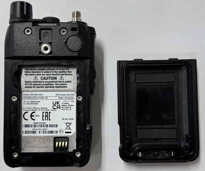
AZ489FT4980
Sep 08, 2026Portable two way radio
Equipment Class
TNF - Licensed Non-Broadcast Transmitter Held to FaceAZ489FT4981
Aug 14, 2026Handheld Portable - TANAPA BPR 45 400-470 MHZ 4W NKP
Equipment Class
TNF - Licensed Non-Broadcast Transmitter Held to Face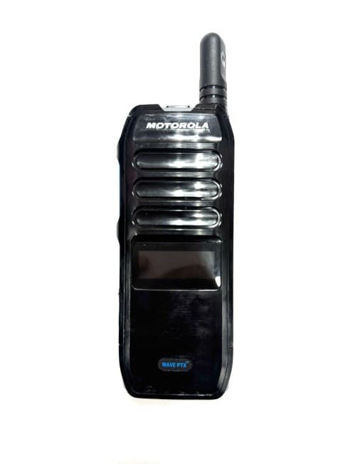
AZ489FT7187
Jul 13, 2026Portable 2-Way Radio with Bluetooth, Bluetooth LE, WIFI 2.4GHz, WIFI 5GHz, LTE
Equipment Class
DSS - Part 15 Spread Spectrum TransmitterAZ499FT6031
May 11, 2026Operation Critical Wireless Earpiece PTT
Equipment Class
DSS - Part 15 Spread Spectrum Transmitter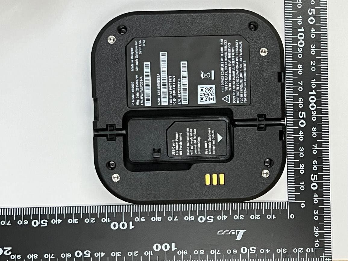
AZ499FT5879
Dec 19, 20252-way Portable Radio with BT, BTLE, WIFI, NFC and LTE
Equipment Class
DSS - Part 15 Spread Spectrum Transmitter