AZ492FT4836Mobile Transmitter
Motorola Solutions, Inc.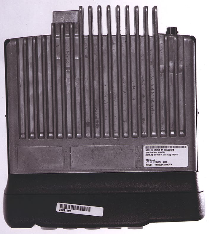
Click to zoom
Application Details
- Equipment Class
- TNB - Licensed Non-Broadcast Station Transmitter
- Date of Grant
- Oct 11, 1999
- Application Purpose
- Original Equipment
- Date of Application
- Jul 26, 1999
- Equipment Note
- Mobile Transmitter
- Frequency Range
- 450.00000000 - 512.00000000
- Company
- Motorola Solutions, Inc.
- Country
- United States
Documents & Files
Document Text
Text extracted from the exhibit documents filed with the FCC. Open a document above to read the original.
Attestation Statements
MOTOROLA INC FCC ID: AZ489FT4836 EXHIBIT 3 STATEMENT OF CERTIFICATION The technical data supplied with this application, having been taken under my supervision is hereby duly certified. The following is a statement of my qualifications: 1) I have received a BSEE degree in Electrical Engineering from University of Michigan Ann Arbor 2) I have 5 years experience in developing, testing and certifying Land Mobile Communications Products. NAME: Mohd. Mirza Noor SIGNATURE: Mohd. Mirza Noor DATE: 6 TH July 1999 POSITION: Senior Engineer I hereby certify that the above application was prepared under my direction and that to the best of my knowledge and belief, the facts set forth in the application and accompanying technical data are true and correct: NAME: NoorAzian Wahab SIGNATURE: NoorAzian Wahab DATE: 6 TH July 1999 POSITION: Engineering Section Manager
Attestation Statements
EXHIBIT 12 RF EXPOSURE INFORMATION In accordance with 47 CFR 2.1093(c) this transmitter may be used in "covered" SMR service so it has been subjected to routine environmental evaluation for RF exposure and found to be compliant with the limits specified in 47 CFR 2.1093(d)(2) using measurements per methods stated in 47 CFR 2.1093(d)(3).
Block Diagram
MOTOROLA INC.FCC ID: AZ492FT4836 EXHIBIT 5 CIRCUIT DESCRIPTION A general description of the overall circuit is covered in the instruction manual. This section provides the description of circuits required by subpart 2.983 of the Commissions’ rules. The following are included: 1) Means for Frequency Stabilization 2) Means for Modulation Limiting 3) Means for Attenuation of Higher Audio Frequencies 4) Means for Attenuation of Spurious Emissions 5) Means for Limiting Output Power 6) Means for Modulation Techniques 7) Means for Transient Frequency Behavior MOTOROLA INC.FCC ID: AZ492FT4836 EXHIBIT 5A 1) Means For Frequency Stabilization Frequency stability is maintained by a reference oscillator/programmable temperature compensation circuit located in the frequency synthesizer IC U4201. The oscillator is a Colpitts design with an amplifier in the IC. The 16.8 MHz crystal Y4261, varactor D4261, and feedback capacitors are external circuitry. A control voltage applied to the varactor via the programmable compensation circuit within U4201maintains the frequency stability to within +/-2.5 ppm over the specified operating temperature range. Frequency tuning, also from the programmable compensation circuit, has 128 steps of resolution. Each 16.8 MHz crystal is numerically coded providing its unique characteristic over the operating temperature range. With the crystal temperature characteristic known, a computed compensation characteristic is programmed into the compensation algorithm. For applications requiring higher frequency stability, an external TCXO module, Y4262, replaces crystal Y4261 and varactor D4261, with the frequency-determining control voltage applied to the frequency adjust pin of the TCXO module. 2) Means for Limiting Modulation Modulation limiting is accomplished within the custom IC, U0221. The limiting action itself occurs at the rails (i.e., 5V and ground). Using an op-amp with feedback, very hard limiting is obtained. The limited modulation signal is then applied to a low-pass splatter filter, and then to an electronic attenuator within U0221 in order to adjust for variations in modulation sensitivities of the frequency synthesizer. The electronic attenuator is controlled by the radio’s microprocessor, U0101. To keep the deviation constant over the RF frequency range & channel bandwidth, the microcomputer adds the proper correction factor to the attenuator. 3) Means for Attenuation Of Higher Audio Frequencies The output of the limiter is applied to a low-pass splatter filter. This filter is a fifth-order switched capacitor filter with the roll-off corner located at 3000 Hz. The output of the low-pass filter is applied to the electronic attenuator before being routed to the modulator. 4) Means For Attenuation Of Spurious Emissions The final stage of the RF power amplifier circuit feeds a low-pass filter in order to attenuate harmonics of the carrier frequency as well as any spurious signals. The filter is a five-pole elliptic design using LC lumped elements. The cast metal chassis forms a compartmentalized shielded enclosure upon which the main circuit board is mounted. A second cast metal compartmentalized shielded enclosure is placed over the main circuit board and secured to the chassis with screws. A conductive elastomeric coating is bonded to the edges of the metal chassis and shield enclosure walls, which come in contact with gold-plated areas of the circuit board when the circuit board and shield are assembled to the chassis. This technique provides very effective and reliable shielding of the various circuits on the main board from each other and from the external environment, minimizing spurious RF radiated emissions. 5) Means For Limiting Output Power Output power is regulated through the use of a forward power detection ALC loop. A directional coupler samples a portion of the forward RF power. The sampled RF is rectified by diode D4451, and the resulting dc voltage is routed to the Power Control IC U4501. This signal is then compared to the preprogrammed reference and the error signal is amplified and used to generate a control voltage to control the bias of the first and second transmitter stages, U4401 and Q4421 respectively. 6) Means Modulation The transmitter is capable of the following types of modulation: i) Modulation of PL (Private Line) - Direct FM tone modulation of 67 Hz to 250.3 Hz at 15% of full system deviation. ii) Modulation of DPL (Digital Private Line) - Direct FM modulation at 134 BPS at 15% of full system deviation. iii) Modulation of DTMF tones at nominally 60% of full system deviation. MOTOROLA INC.FCC ID: AZ492FT4836 EXHIBIT 5 Direct FM of PL or DPL is generated by a 6-bit D/A converter contained within U0221. The frequency-determining clock signal is generated by the radio microcomputer. The modulation signal is processed through a five pole switched capacitor filter. The output of the filter is input to the electronic attenuator circuit. The microcomputer adjusts the attenuator to compensate for modulation sensitivity variations of the synthesizer & channel bandwidth ensuring 15% of full system deviation for PL and DPL. DTMF tones are generated by the audio processing IC, U0221. The tones are routed and processed in the same manner as the voice signals. 7) Means of Transient Frequency Behavior The effects of VCO frequency shifts due to transmitter key-up and de-key impedance variations are minimized through the use of a multiple-stage transmitter lineup with resistive isolation pads between various stages, including a pad between the output of the VCO/buffer IC and the input of the transmitter circuit. Additionally, the value of the DAC which controls output power is gradually raised during transmitter key-up and lowered during de-key, shaping the transmitter attack and decay characteristics by gradually changing the power control voltage. Finally, a pre-bias voltage is applied to the RF detector diode in the directional coupler so that the p…
Text truncated - open the document above for the full version.
Cover Letter(s)
MOTOROLA INC FCC ID: AZ492FT4836 ______________________________________________________________________________ Radio Products Group 8000 West Sunrise Boulevard, Fort Lauderdale, Florida 33322. (954) 723-5000 LIST OF EXHIBITS DESCRIPTIONEXHIBITFCC REFERENCE l.Cover Letter12.1033 llIdentification label information22.983-(f) & General Information2A2.981-(c) & 2.1061 1. Production Plans 2. Application References 3. Data Submittal Procedures IIICertification Of Data32.907 IVExternal Photographs42.983-(g) VBlock Diagrams or Circuit Descriptions52.983-(d)-10,11 1. Frequency Stabilization 2. Modulation Limiting 3. Attenuation Of Higher Audio Frequencies 4. Attenuation Of Spurious Emissions 5. Limiting Output Power 6. Modulation Techniques 7. Transient Frequency Behavior VISchematic Diagrams62.983-(d)-7 VIITest Report7 1. Data Index7 2. RF Output Data7A2.985 (a) 3. Modulation Characteristics2.987 (a) a) Audio Response7B b) Low Pass Filter Response7C c) Modulation Limiting7D 4. Occupied Bandwidth7E2.989 5. Conducted Spurious Emissions7F2.991 6. Radiated Spurious Emissions7G2.993 7. Frequency Stability (Temp. & Supply Volt) 7H & 7I2.995 8. Transient Frequency Behavior 7J2.2.19(EIA/TIA SP-2218) VIIITest Set-Up Procedures8 a) Test Equipment Used b) Method Of Measurements c) Emission Designator Information 1XInstruction Manual9 XInternal Photograph(s)102.983-(g) XIParts List & Tune-up Procedures11 & 11A2.983-(d)-6 & 2.983-(d)-9 XIIRF Exposure Information12 XIIIOperational Description13 a) Technical Characteristics2.983-(d)-1,2,3,4,5 b) Application MOTOROLA INC FCC ID: AZ492FT4836 ______________________________________________________________________________ Radio Products Group 8000 West Sunrise Boulevard, Fort Lauderdale, Florida 33322. (954) 723-5000 Date:July 27, 1999. Authorization & Evaluation Division Federal Communications Commission Laboratory 7435 Oakland Mills Road Columbia, MD 21046 Subject: Application for Certification of Transmitter with FCC ID: AZ492FT4836. Attention: Frank Coperich. Gentlemen: Motorola Inc, 8000 West Sunrise Boulevard, Fort Lauderdale, Florida, herein submits it’s application for Certification of the subject transmitter. This transmitter is primarily intended for use in a mobile radio application with capabilities for communications with a transmit power of 25--48 Watt. The Power is variable 52% of the value listed (25--48 Watt). The subject transmitter complies with Section 90.203 of the rules in that the operator cannot directly program transmit frequencies using only the unit's normally accessible external controls. Enclosed is a complete Certification application. Contact me at (954) 723-5793 if you require any additional information. Sincerely, Mike Ramnath FCC Liaison Email: [email protected] Fax (954) 723-4794
External Photos
MOTOROLA INC.FCC ID: AZ492FT4836 EXHIBIT 4 EXTERNAL PHOTOGRAPHS 1EXHIBIT 4ATransceiver General View, Version 3 “Preferred” Control Head 2EXHIBIT 4BModel-Dependent Control Head Configurations 3EXHIBIT 4CTransceiver Bottom View showing FCC Label 4EXHIBIT 4D Model Description MOTOROLA INC.FCC ID: AZ492FT4836 EXHIBIT 4B Transceiver General View, Version 3 “Preferred” Control Head MOTOROLA INC.FCC ID: AZ492FT4836 EXHIBIT 4 C “ Plain ” Control Head MOTOROLA INC.FCC ID: AZ492FT4836 EXHIBIT 4 C “ Prime ” Control Head MOTOROLA INC.FCC ID: AZ492FT4836 EXHIBIT 4 C Transceiver Bottom View showing FCC Label Exploded View of FCC Label FCC Label Location MOTOROLA INC.FCC ID: AZ492FT4836 EXHIBIT 4 C MODEL DESCRIPTION Model NumberNameplateDescription AZM25SKC9AA1AN-Plain MDM25SKC9AA1AN-Plain LAM25SKC9AA1AN-Plain AAM25SKC9AA1ANCDM 550Plain AZM25SKD9AA2AN-Popular MDM25SKD9AA2AN-Popular LAM25SKD9AA2AN-Popular AAM25SKD9AA2ANCDM 750Popular AZM25SKF9AA5AN-Preferred MDM25SKF9AA5AN-Preferred LAM25SKF9AA5AN-Preferred AAM25SKF9AA5ANCDM 1250Preferred AZM25SKN9AA8AN-Prime MDM25SKN9AA8AN-Prime LAM25SKN9AA8AN-Prime AAM25SKN9AA8AN-Prime
ID Label/Location Info
MOTOROLA INC FCC ID: AZ492FT4836 EXHIBIT 2 IDENTIFICATION LABEL LOCATION XSee the Attached Photograph or Sketch Back of Radio Back of Radio under Belt Clip TYPE XThe label is a paper polyester firm laminate with a pressure sensitive adhesive backing. The adhesive is a permanent type acrylic with a minimum peel strength of 40 oz/inches. The label is laser etched into the Urethane paint, exposing the Nickel plating on the Zamak casting substrate. Since no adhesive Is required, the label is permanent and tamper-proof. (**-NOTE- The label attached below is a paper polyester film laminate, as described above. This is just for sample purposes, as the actual label is laser etched into the casting) MARKINGS (TEXT) See the Attached Photograph XLabel Attached Below See Attached Drawing MOTOROLA INC FCC ID: AZ492FT4836 EXHIBIT 2a GENERAL INFORMATION l.Production Plans -- Pursuant 2.981 ( c ) Quantity production is planned ll.Application References -- Pursuant 2.1061 EIA/TIA-603 Land Mobile FM or PM Communications Equipment Measurement and Performance Standards Code of Federal Regulations Title 47, Part 2, Sec. 2.983-2.999 and Part 90, Sec.90.210 lll.Data Submittal Procedure: Data is supplied in accordance with Part 2, Sub-part J of the Commissions’ Rules. The intended use of this transceiver includes applications covered in the Code of Federal Regulations Title 47, Parts 22, 74, and 90.
Internal Photos
MOTOROLA INC.FCC ID: AZ492FT4836 EXHIBIT 10 INTERNAL PHOTOGRAPHS 1EXHIBIT 10-ATransceiver Top View (with decorative housing cover removed, control head attached) 2EXHIBIT 10-BTransceiver Top View with Top Shield Removed (top shield placed along-side the chassis, solder-side of board showing, control head attached). 3EXHIBIT 10-CTransceiver Top View with Circuit Board and Control Head Removed (circuit board placed along side the chassis, component-side of board showing). MOTOROLA INC.FCC ID: AZ492FT4836 EXHIBIT 10A Transceiver Top View (with decorative housing cover removed, control head attached) MOTOROLA INC.FCC ID: AZ492FT4836 EXHIBIT 10C Transceiver Top View with Top Shield Removed (top shield placed along-side the chassis, solder-side of board showing, control head attached). MOTOROLA INC.FCC ID: AZ492FT4836 EXHIBIT 10C Transceiver Top View with Circuit Board and Control Head Removed (circuit board placed along side the chassis, component-side of board showing)
Operational Description
MOTOROLA INC FCC ID: AZ492FT4836 EXHIBIT 13-1 OPERATIONAL DESCRIPTION A.Transmitter Technical Characteristics -- Pursuant 2.983 (d) a. RF Power Output:25W to 48W Variable Power b. Transmit Frequency Range:450 – 512 MHz c. Receive Frequency Range:450 – 512 MHz d. Frequency Stability:+/- 2.0 PPM e. Emissions16K0F3E & 11K0F3E (See Exhibit 8-5) f. Spurious Emissions-74dBc (25W) & -76.8dBc (48W) g. DC Voltage and Current into13.6 VDC the final RF amplifier stage/stages11A B.Transmitter Application This transmitter is primarily intended for use in a mobile environment. It is characterized by the following features, options, and accessories. a. Power Supply Available: i. Vehicular battery, or AC-DC Converter b. Antenna Available: i. Whip Antenna ii. Roof Top Antenna iii. ¼ wave Antenna iv. Other External 50-ohm Antenna c. Squelch Type Available: i. Carrier Squelch ii. Tone “Private Line” iii. Digital “Private Line” iv. DTMF d. Microphone - Control: i. Hand-held Microphone ii. Hand-held Conventional with DTMF iii. Base Station Desk Top iv. Telephone Style Handset e. Maximum Transmit Channel Capability: i. 4 to 160 Channels, depending on model. f. Housing: The transmitter is enclosed in a metal, shielded chassis as shown in the accompanying photographs. The transmitter circuitry is contained on a single printed circuit board that is mounted to a cast metal chassis that also serves as a heatsink. A cast metal shield cover is placed over the printed circuit board and secured to the chassis with screws. Interior walls in both the chassis and shield cover form compartments that provide isolation between various circuit blocks. The frequency synthesizer, vco/buffers, transmitter stages, and low-pass harmonic filter are each contained in individual, isolated compartments. A conductive elastomeric coating is bonded to the edges MOTOROLA INC FCC ID: AZ492FT4836 EXHIBIT 13-2 of the metal chassis and shield enclosure walls, which come in contact with gold-plated areas of the circuit board when the circuit board and shield are assembled to the chassis. A decorative plastic housing encloses the top and sides of the chassis. The operating controls, indicators and supporting circuitry are contained in a separate plastic housing which is mounted to the front of the chassis. g. Other Options: i. Time out Timer h. Available Accessories: GKN6272AExternal alarm relay GLN7318ADesktop mounting tray w/out speaker GLN7323AExternal PTT/ emergency foot switch GLN7324ALow profile mounting trunnion GLN7326ADesktop mounting tray w/speaker GTF347BMobile Programming Cable HAE4003UHF 450-470 MHz, ¼ Wave Roof Antenna HAE4011UHF 450-470 MHz, 3.5 dB Gain Roof Antenna HAE4019UHF 450-470 MHz, 5 dB Gain Roof Antenna HAE4004UHF 470-512 MHz, ¼ Wave Roof Antenna HAE4012UHF 470-494 MHz, 3.5 dB Gain Roof Antenna HKN4013UHF 494-512 MHz, 5 dB Gain Roof Antenna HKN9019BEnhanced connector HKN9402A12V Battery Power Cable 25-45W HKN9557AMini-UHF to PL259 cable HLN3333B RICK with Mounting Bracket HLN3948BRICK with Mounting Tray HLN8097A Removable slide mount HLN9457AAccessory connector Kit HLN9725BVoice Storage Option Board HLN9742AAdaptor Flashing HMN3000BBlack Desk Microphone HPN4001BDesktop power supply, 25-60W HSN8145AExternal speaker 7.5W L3144AC200 Basic Extended Local Control (Eng Manual) L3145AC200 Basic DC Remote Control (Eng Manual) L3146AC200 Basic Tone Remote Control (Eng Manual) L3147AC200 Advanced Extended Local Control (Eng Manual) L3148AC200 Advanced DC Remote Control (Eng Manual) L3149AC200 Advanced Tone Remote Control (Eng Manual) NTN7373ARlinecord (3060665A04) packaged NTN7374ARUS linecord (3060665A05) packaged NTN7375ARUS linecord (3002120F02) packaged 0902105F01BNC Connector AAHLN9725BVoice Storage Option Bd (w/NA/LA Manual) HLN9725AVoice Storage Option Bd (w/o Manual) MOTOROLA INC FCC ID: AZ492FT4836 EXHIBIT 13-3 AAHLN9729ADTMF Decode Option Bd (w/NA/LA Manual) HLN9729ADTMF Decode Option Bd (w/o Manual) AAHLN9726ATranscrypt Option Bd (w/NA/LA Manual) HLN9726ATranscrypt Option Bd (w/o Manual) AAHLN9727AScrambler Option Bd (w/NA/LA Manual) HLN9727AScrambler Option Bd (w/o Manual) AAHLN9728ASmartrunk Option Bd (w/NA/LA Manual) MDHLN9728ASmartrunk Option Bd (w/o Manual) j. Programmability: Programming is accomplished by the use of an IBM PC computer or equivalent, a Radio Interface Box, and Radio Service Software. Adjustment of the transmitter, including programming of the channel frequencies, output power adjustment, frequency adjustment, and deviation adjustment are performed in this manner. NOTE: The transmitter is NOT programmable by the operator. i. The minimum voltage for the micro-P to operate is 2V.
Parts List/Tune Up Info
MOTOROLA INC.FCC ID: AZ492FT4836 EXHIBIT 11-2 FUNCTION OF RF SEMICONDUCTORS AND OTHER ACTIVE DEVICES SCHEMATICPARTCIRCUITOPERATINGINDUSTRY KEYNUMBERAPPLICATIONFREQUENCYEQUIVALENT CR43014805649Q13RX VCO FREQ CONTROL405.15-467.15 MHz1SV228 CR43024862824C01RX VCO FREQ CONTROL405.15-467.15 MHz1SV229 CR43034862824C01RX VCO FREQ CONTROL405.15-467.15 MHz1SV229 CR43114802245J22TX VCO FREQ CONTROL450-512 MHz1T363 CR43214862824C01TX VCO MODULATOR450-512 MHz1SV229 D01014880236E05DATA SWITCH230 kHz MMBD301 D01514813833C02DC SWITCHDC MMBD6100 D01794813833C02CLAMP DC MMBD6100 D03014802245J47DC SWITCHDCRB471E D02014802245J47DC SWITCHDCRB471E D06214813833C02DC SWITCHDCMMBD6100 D06514813833C02DC SWITCHDCMMBD6100 D06604813833C02DC SWITCHDCMMBD6100 D06614813833C02DC SWITCH DCMMBD6100 D31014880154K03CLIPPER44.85 MHzMMBD353 D40014862824C01FRONT END FILTER 450-512 MHz1SV229 TUNING D40024862824C01FRONT END FILTER 450-512 MHz1SV229 TUNING D40034880154K03CLIPPER450-512 MHzMMBD353 D40044862824C01FRONT END FILTER 450-512 MHz1SV229 TUNING D40054862824C01FRONT END FILTER 450-512 MHz1SV229 TUNING D40514886143B01DOUBLE BALANCED 44.85-512 MHzSMS3927-99 MIXER D42014802233J09VOLTAGE MULTIPLIER1.05 MHzIMN10 D42614802245J22REF OSC FREQ CONTROL16.8 MHz 1T363 D44514880236E05FORWARD POWER 450-512 MHzMMBD301 DETECTOR D44524880236E05REVERSE POWER 450-512 MHz MMBD301 DETECTOR D44534880236E05TEMPERATURE 450-512 MHz MMBD301 COMPENSATION D44714802482J02RF PIN SWITCH 450-512 MHz MA4P959 D44724802482J02RF PIN SWITCH450-512 MHzMA4P959 Q01104880048M01DC SWITCH DC DTC144EKA Q01514880048M01DC SWITCHDCDTC144EKA Q01734880052M01DC SWITCH DCRXT-A28 Q01774880048M01DC SWITCHDCDTC144EKA Q01814880048M01DC SWITCHDC DTC144EKA Q01834880048M01DC SWITCHDCDTC144EKA Q01854880048M01DC SWITCHDC DTC144EKA Q02714813824A10DC SWITCHDCMMBT3904 Q03314805921T02DATA SWITCH1 MHzFMC2A Q06414880048M01DC SWITCH DCDTC144EKA Q06614805921T02DC SWITCH DCFMC2A Q06624813824A10DC SWITCHDCMMBT3904 Q06634880048M01DC SWITCHDCDTC144EKA Q31014813827A07I-F AMPLIFIER44.85 MHz MMBR941 Q31024813827A07I-F AMPLIFIER44.85 MHzMMBR941 Q31514880048M01DC SWITCHDCDTC144EKA Q31524880048M01DC SWITCHDCDTC144EKA Q31554880048M01AUDIO SWITCHAUDIODTC144EKA Q40034813827A07RF AMPLIFIER450-512 MHzMMBR941 Q43014805218N63RX VCO358.15-425.15 MHzBFQ67W Q43324813827A07RX VCO BUFFER358.15-425.15 MHzMMBR941 Q43334802245J50DC SWITCHDCUMC5N Q44215105385Y70TX PRE-DRIVER STAGE450-512 MHz 85Y70 Q44314805537W01TX DRIVER STAGE450-512 MHzMRF5015 Q44414880225C30TX FINAL POWER AMP.450-512 MHzMRF650 MOTOROLA INC.FCC ID: AZ492FT4836 EXHIBIT 11-2 FUNCTION OF RF SEMICONDUCTORS AND OTHER ACTIVE DEVICES SCHEMATICPARTCIRCUITOPERATINGINDUSTRY KEYNUMBERAPPLICATIONFREQUENCYEQUIVALENT Q44714880048M01DC SWITCHDCDTC144EKA Q44724805128M27CONSTANT CURRENT DC BSR33 SINK Q44734813824A10POWER CONTROL DC AMPDCMMBT3904 U01015102226J56MICROPROCESSOR38.4 kHz-7.4 MHzMC68HC11FL0 U01115102463J47EEPROM 1 MHzX25320_2.7V U01215186137B01FLASH ROM1.85 MHzAT49F040 U01225185963A21SRAM 1.85 MHz63A21 U01255105625U34UART 1.85 MHzCDP65C51A U01415113805A30DECODER/DEMUX5 kHzMC74HC138A U02115183222M49AUDIO AMPLIFIERAUDIOMC3403 U02215185963A53AUDIO FILTER 16.8 MHz63A53 U02515113806A20AUDIO GATE AUDIOMC14053B U02715109699X01AUDIO POWER AMPLIFIER AUDIOTDA1519C U03015102463J53VOICE STORAGE1 MHzISD33000 U03415180932W01AUDIO AMPLIFIER AUDIOLM2904 U03425105750U28AUDIO GATEAUDIO TC4S66F U03515102463J40VOLTAGE REGULATOR DCLP2951ACMM-3.3 U06115183308X01VOLTAGE REGULATORDCLM2941 U06415183308X01VOLTAGE REGULATORDCLM2941 U06515113816A07VOLTAGE REGULATORDCMC78M05 U06525113815A02RESET MONITOR DCMC33064 U06534805921T02DATA SWITCH1 MHzFMC2A U31015186144B01RECEIVER SYSTEM455 kHz-44.85 MHzSA616 U31115113805A86RF SWITCH455 kHzMC74HC4066 U31155113805A86RF SWITCH 455 kHzMC74HC4066 U42015185963A27FREQUENCY 1.05-470 MHz63A27 SYNTHESIZER U42115105469E65VOLTAGE REGULATORDC LP2951C U43015105750U54TX VCO/RX BUFFER/TX 405.15-512 MHz50U54 BUFFER U44015105109Z67GAIN CONTROLLED 450-512 MHz09Z67 AMPLIFIER U45015185765B01TX POWER CONTROL1 MHzH99S-4 U45025185963A15TEMPERATURE SENSORDCLM50 VR01514813830A15DC LEVEL-SENSING DCMMBZ5232B SWITCH VR05014805656W09ESD PROTECTION DCMMQA20VT1 VR05034805656W09ESD PROTECTIONDC MMQA20VT1 VR05044813830A40ESD PROTECTIONDCMMBZ5257B VR05054805656W09ESD PROTECTIONDCMMQA20VT1 VR05094813830A40ESD PROTECTIONDCMMBZ5257B VR05104813830A40ESD PROTECTIONDCMMBZ5257B VR05214813830A15ESD PROTECTIONDCMMBZ5232B VR05224813830A15ESD PROTECTIONDCMMBZ5232B VR05374813830A15ESD PROTECTIONDCMMBZ5232B VR05414813830A27ESD PROTECTIONDCMMBZ5244B VR06014813832C77TRANSIENT SUPPRESSORDCMR2835S VR06214813830A14VOLTAGE REGULATOR DCMMBZ5231B VR06714813830A14VOLTAGE REGULATOR DCMMBZ5231B VR44714813830A15CURRENT SINK DCMMBZ5232B REFERENCE COMMENTS: The Motorola designators are special code numbers for active devices used in Motorola radios. These devices are either identical or derived from the device family listed under Industry Equivalent, by the manufacturer or are proprietary to Motorola. Service people do not have access to any cross-references or given any information on proprietary devices and are prevented from making unauthorized substitution. MOTOROLA INC.FCC ID: AZ492FT4836 EXHIBIT 11A-1 TUNING PROCEDURES Tune up Information All transmitter adjustments are performed by electronic means. The transmitter contains no electromechanical components for the purpose of transmitter tuning or adjustment. The tuning elements that are used for transmitter adjustment are: LocationType of ElementFunction U0101MicrocomputerSupplies data to Audio Filter IC, Fractional-N Synthesizer, Temperature Compensated Crystal Oscillator, and Power Control IC for Transmitter Modulation, Frequency and Power Adjustment U4201Programmable AttenuatorVCO Modulation Sensitivity U4201Programmable AttenuatorReference Modulation Sensitivity U0221Programmable AttenuatorDeviation Adjustment U4201Temperature CompensatedTransmitter Frequency Adjustment Crystal Oscillator U4501Digital to Analog ConverterTransmitter Power…
Text truncated - open the document above for the full version.
Schematics
MOTOROLA INC FCC ID: AZ489FT4836 EXHIBIT 6 SCHEMATIC DIAGRAMS The schematic diagrams are as follows: 1Basic Transmitter 2Power Control IC 3 Pre-Driver 4Driver 5Controller Stage 6Power Amplifier MOTOROLA INC FCC ID: AZ489FT4836 EXHIBIT 6 MOTOROLA INC FCC ID: AZ489FT4836 EXHIBIT 6-1 1)BASIC TRANSMITTER MOTOROLA INC FCC ID: AZ489FT4836 EXHIBIT 6-2 2)POWER CONTROL IC MOTOROLA INC FCC ID: AZ489FT4836 EXHIBIT 6-3 3) PRE-DRIVER MOTOROLA INC FCC ID: AZ489FT4836 EXHIBIT 6-4 4)DRIVER MOTOROLA INC FCC ID: AZ489FT4836 EXHIBIT 6-5 5)CONTROLLER STAGE MOTOROLA INC FCC ID: AZ489FT4836 EXHIBIT 6-6 6)POWER AMPLIFIER
Test Report
MOTOROLA INC. FCC ID: AZ492FT4836 EXHIBIT 7 SUBMITTED MEASURED DATA AND METHOD OF MEASUREMENT MEASUREMENTEXHIBITNUMBER OF PAGES IRF Power Output7A 1 IIAudio Response7B 2 IIILow Pass Filter Response7C 2 IVModulation Limiting7D 6 V Occupied Bandwidth7E 18 V1Conducted Spurious Emissions7F4 VIIRadiated Spurious Emissions7G2 VIIIFrequency Stability A. Temperature7H 1 B. Supply Voltage7I 1 IXTransient Frequency Behavior7J2 MOTOROLA INC. FCC ID: AZ492FT4836 EXHIBIT 7-A RF Power Output - Measured Data The supply voltage to the transmitter was set to 13.6 volts DC. The RF output power was measured with the indicated voltage and current applied into the final RF amplifying device. RF POWER OUTPUT 48W, FREQUENCY 450.100 MHz. Measured RF Output Power:46.8 WATTS Measured DC Voltage:13.38 VOLTS Measured DC Current:5.84 AMP Measured DC Input Power:78.14 WATTS RF POWER OUTPUT 48W, FREQUENCY 481.100 MHz. Measured RF Output Power: 46.8 WATTS Measured DC Voltage:13.4 VOLTS Measured DC Current:5.42 AMP Measured DC Input Power:72.63 WATTS RF POWER OUTPUT 48W, FREQUENCY 511.900 MHz. Measured RF Output Power:46.8 WATTS Measured DC Voltage:13.41 VOLTS Measured DC Current:5.24 AMP Measured DC Input Power:70.27 WATTS RF POWER OUTPUT 25W, FREQUENCY 450.100 MHz. Measured RF Output Power:29.5 WATTS Measured DC Voltage:13.44 VOLTS Measured DC Current:4.28 AMP Measured DC Input Power:57.52 WATTS RF POWER OUTPUT 25W, FREQUENCY 481.100 MHz. Measured RF Output Power:29.5 WATTS Measured DC Voltage:13.46 VOLTS Measured DC Current:3.92 AMP Measured DC Input Power:52.76 WATTS RF POWER OUTPUT 25W, FREQUENCY 511.900 MHz. Measured RF Output Power:29.5 WATTS Measured DC Voltage:13.47 VOLTS Measured DC Current:3.62 AMP Measured DC Input Power: 48.76 WATTS MOTOROLA INC. FCC ID: AZ492FT4836 EXHIBIT 7B -1 MOTOROLA INC. TRANSMITTER AUDIO RESPONSE CHARACTERISTIC MODULATION LEVEL vs. AUDIO FREQUENCY =============================================================================== Xmtr Type : AZ492FT4836 Log Page : --- Date : 16 th June 1999 Signature : SF Ooi Frequency: 481.100Mhz Channel Spacing: 25KHz -40.0 -35.0 -30.0 -25.0 -20.0 -15.0 -10.0 -5.0 0.0 5.0 10.0 15.0 100.01000.010000.0 Audio Frequency in Hz Modulation Level in dB MOTOROLA INC. FCC ID: AZ492FT4836 EXHIBIT 7B-2 MOTOROLA INC. TRANSMITTER AUDIO RESPONSE CHARACTERISTIC MODULATION LEVEL vs. AUDIO FREQUENCY =============================================================================== Xmtr Type : AZ492FT4836 Log Page : --- Date : 16 th June 1999 Signature : SF Ooi Frequency: 481.100Mhz Channel Spacing: 12.5KHz -40.0 -35.0 -30.0 -25.0 -20.0 -15.0 -10.0 -5.0 0.0 5.0 10.0 15.0 100.01000.010000.0 Audio Frequency in Hz Modulation Level in dB MOTOROLA INC. FCC ID: AZ492FT4836 EXHIBIT 7C-1 MOTOROLA INC. TRANSMITTER POST - LIMITER ROLL OFF RESPONSE FILTER OUTPUT vs. AUDIO FREQUENCY ================================================================================= Xmtr Type : AZ492FT4836 Log Page : --- Date : 16 th June 1999 Signature : SF Ooi Frequency : 481.100Mhz Channel Spacing : 25KHz -60.00 -50.00 -40.00 -30.00 -20.00 -10.00 0.00 10.00 100.001000.0010000.00100000.00 Audio Frequency in Hz dB MOTOROLA INC. FCC ID: AZ492FT4836 EXHIBIT 7C-2 MOTOROLA INC. TRANSMITTER POST - LIMITER ROLL OFF RESPONSE FILTER OUTPUT vs. AUDIO FREQUENCY ================================================================================= Xmtr Type : AZ492FT4836 Log Page : --- Date : 16 th June 1999 Signature : SF Ooi Frequency : 481.100Mhz Channel Spacing : 12.5KHz -60.00 -50.00 -40.00 -30.00 -20.00 -10.00 0.00 10.00 100.001000.0010000.00100000.00 Audio Frequency in Hz dB MOTOROLA INC. FCC ID: AZ492FT4836 EXHIBIT 7D-1 MOTOROLA INC. CARRIER SQUELCH AUDIO INPUT LEVEL vs. DEVIATION ================================================================================== Xmtr Type : AZ492FT48306 Log Page : --- Date : 16 th June 1999 Signature : SF Ooi Frequency : 481.100Mhz Channel Spacing : 25 KHz 0 500 1000 1500 2000 2500 3000 3500 4000 4500 5000 5500 6000 -20-15-10-505101520 Audio Input Level (dB) Deviation in Hz 1000HZ 300HZ 3000HZ Limit Spec limit: 5Khz MOTOROLA INC. FCC ID: AZ492FT4836 EXHIBIT 7D-2 MOTOROLA INC. TONE WITH “PL” AUDIO INPUT LEVEL vs. DEVIATION ================================================================================== Xmtr Type : AZ492FT4836 Log Page : --- Date : 16 th June 1999 Signature : SF Ooi Frequency : 481.100Mhz Channel Spacing : 25KH 0 500 1000 1500 2000 2500 3000 3500 4000 4500 5000 5500 6000 -20-15-10-505101520 Audio Input Level (dB) Deviation in Hz 1000HZ 300HZ 3000HZ Limit Spec limit: 5Khz MOTOROLA INC. FCC ID: AZ492FT4836 EXHIBIT 7D-3 MOTOROLA INC. TONE WITH “DPL” AUDIO INPUT LEVEL vs. DEVIATION ================================================================================= Xmtr Type : AZ492FT4836 Log Page : --- Date : 16 th June 1999 Signature : SF Ooi Frequency : 481.100Mhz Channel Spacing : 25KHz 0 500 1000 1500 2000 2500 3000 3500 4000 4500 5000 5500 6000 -20-15-10-505101520 Audio Input Level (dB) Deviation in Hz 1000HZ 300HZ 3000HZ Limit Spec limit: 5Khz MOTOROLA INC. FCC ID: AZ492FT4836 EXHIBIT 7D-4 MOTOROLA INC. CARRIER SQUELCH AUDIO INPUT LEVEL vs. DEVIATION =================================================================================…
Text truncated - open the document above for the full version.
Contact Information
Applicant
Deanna Zakharia(Regulatory Compliance Manager)
Technical Contact
Motorola IncMike Ramnath
[email protected]954-723-5793
8000 West Sunrise Blvd · Ft. Lauderdale, Florida · United States
Technical Specifications
| # | Rule Parts | Frequency Range | Power Output | Emission | Tolerance |
|---|---|---|---|---|---|
| 2 | 22,74,9 | 450 MHz - 512 MHz | 48 W | 16K0F3E | 2 ppm |
Other Applications from Motorola Solutions, Inc.
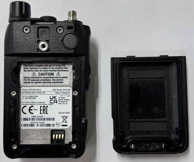
AZ489FT4980
Sep 08, 2026Portable two way radio
Equipment Class
TNF - Licensed Non-Broadcast Transmitter Held to FaceAZ489FT4981
Aug 14, 2026Handheld Portable - TANAPA BPR 45 400-470 MHZ 4W NKP
Equipment Class
TNF - Licensed Non-Broadcast Transmitter Held to Face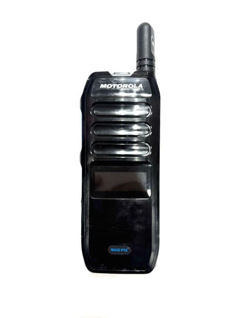
AZ489FT7187
Jul 13, 2026Portable 2-Way Radio with Bluetooth, Bluetooth LE, WIFI 2.4GHz, WIFI 5GHz, LTE
Equipment Class
DSS - Part 15 Spread Spectrum TransmitterAZ499FT6031
May 11, 2026Operation Critical Wireless Earpiece PTT
Equipment Class
DSS - Part 15 Spread Spectrum Transmitter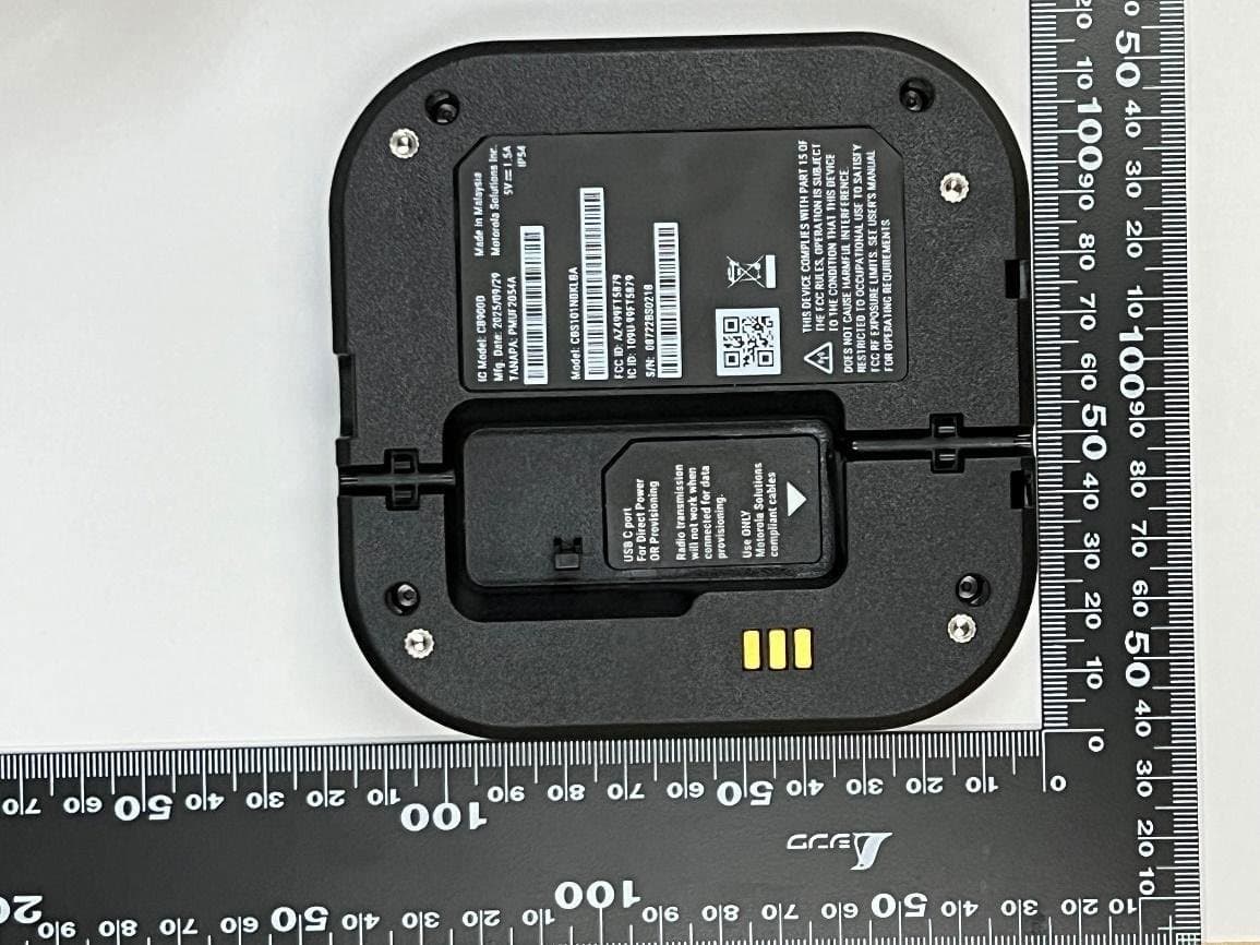
AZ499FT5879
Dec 19, 20252-way Portable Radio with BT, BTLE, WIFI, NFC and LTE
Equipment Class
DSS - Part 15 Spread Spectrum Transmitter