B5KAKRC1311010-2Broadband GSM Base station transceiver
Ericsson Radio Systems AB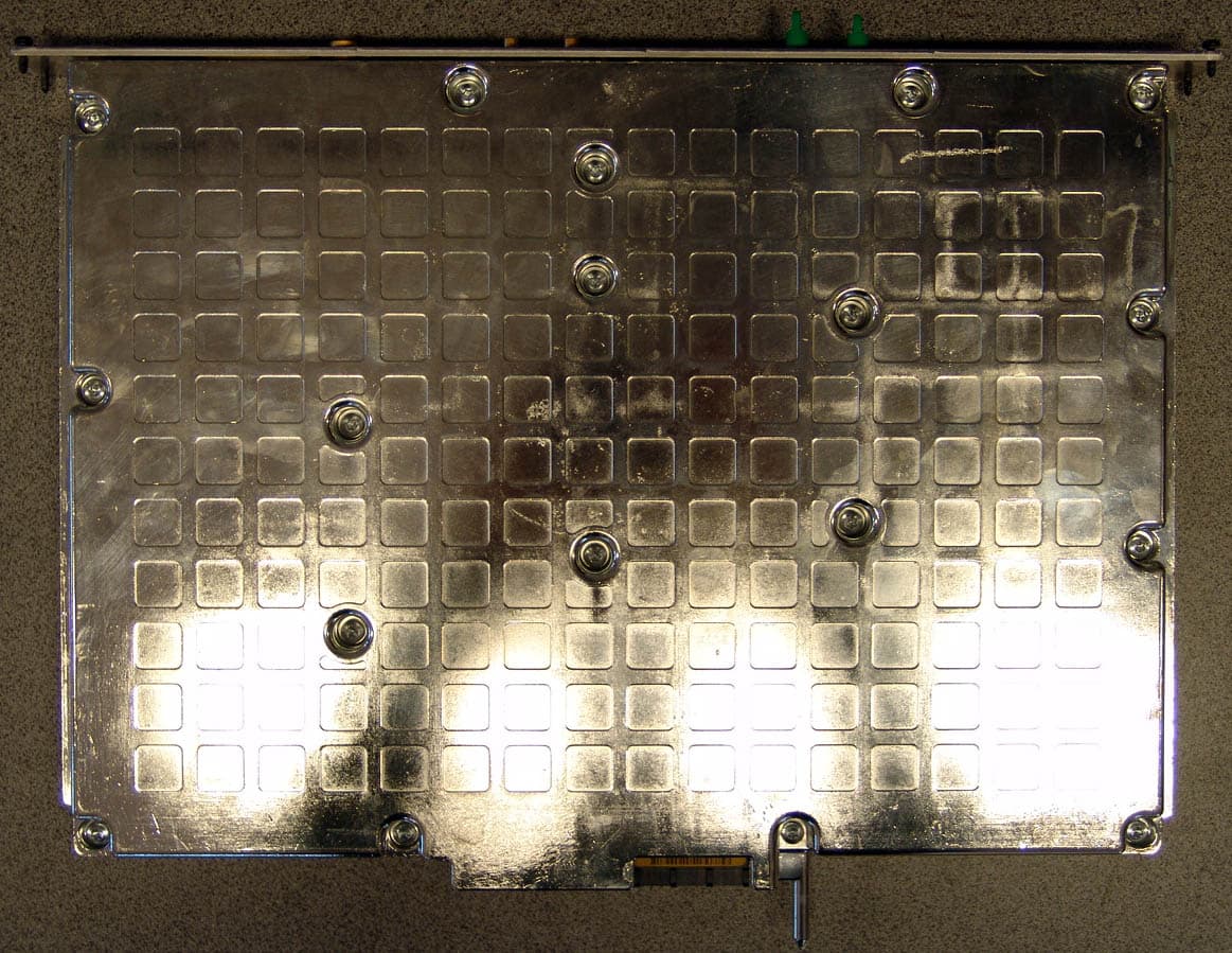
Click to zoom
Application Details
- Equipment Class
- TNB - Licensed Non-Broadcast Station Transmitter
- Date of Grant
- Apr 04, 2005
- Application Purpose
- Original Equipment
- Date of Application
- Apr 04, 2005
- Equipment Note
- Broadband GSM Base station transceiver
- Frequency Range
- 869.20000000 - 893.80000000
- Company
- Ericsson Radio Systems AB
- Country
- Sweden
Documents & Files
Document Text
Text extracted from the exhibit documents filed with the FCC. Open a document above to read the original.
Block Diagram
Open EXHIBIT 4 1 (2) Prepared (also subject responsible if other) No. EAB/RBI/R Per Helmersson B5KAKRC1311010-2 Approved Checked Date Rev Reference KI/EAB/RBI/R (P Helmersson) 2005-03-11 A EXHIBIT 4 - COVER SHEET 1 Block diagrams Contents 1 Block diagrams ....................................................................................1 1.1 Block Diagram TBU 800 MHz GMSK ROA 128 1360/2......................2 Sheet 4 5 6 7 8 9 10 11 12 13 14 15 16 A B C D E F G H I J K Prepared (also subject responsible if other) References Doc respons/Approved Date Rev Product name Document no A B C D E F G H 1234567891011 I J K 12 13 14 15 16 123 +1.2V N0007 TX1 +7V +7V -5V +7V_LTU -5V MID_VOLT +7V REF_RANGE_5900 N0008 TX_BACKEND +1.2V +3.3V +3.3V_RX +3.3V +7V +1.2V TX2 N0007 ERA/RBR/F (Göran Wikström)MGC BS 2002.1w A ERAMMSV 2005-01-17 1911-ROA 128 1360/2 Ux +3.3V+7V +7V -5V +3.3V_RX +3.3V+7V+1.8V +7V INT_12V +3.3V 1(1) dTRU TBU 800 HcHc +3.3V+1.2V +7V +3.3V +3.3V +7V_LTU REF_RANGE_3000 CPUSYSTEM N0001 CPUSYSTEM N0002DCDC_BOOSTER REF_RANGE_700-900 ROZ 104 224/1 N0004 SPARC2 ROZ 104 223/1 REF_RANGE_6000 ROZ 104 222/1 REF_RANGE_5000 N0003 SPARC1 RX FRONTEND INX 106 145/1 REF_RANGE_1000 RX_FRONTEND N? N0009 +7V N0006 LTU REF_RANGE_500 ROZ 104 225/1 +1.8V N0011
Cover Letter(s)
Open EXHIBIT 13 1 (2) Prepared (also subject responsible if other) No. EAB/RBI/R Per Helmersson and Björn Rosenquist Approved Checked Date Rev Reference KI/EAB/RBI/R (P Helmersson) 2005-04-05 C B5KAKRC1311010-2 Federal Communications Commission Authorization & Evaluation Division 7435 Oakland Mills Road Columbia, Maryland 21046 Attention: Equipment Authorization Branch SP Sveriges Provnings- och ForskningsInstitut Brinellgatan 4 Box 857 S-501 15 Borås Sweden March 23, 2005 Subject: Certification for FCC ID: B5KAKRC1311010-2 Gentlemen; Ericsson AB requests a Grant of Certification (Type Acceptance) for the above-mentioned FCC Identifier. This base station transceiver is designed for use in the GSM 800 MHz cellular telephone system. The transmitter will operate from 869.2 to 893.8 MHz. The receiver circuit supports 824.2 to 848.8 MHz. The base station operates in the 800 MHz broadband Cellular services as per 47 CFR Part 22 subpart H, 22.901 (d). It meets the requirements of GSM1900 11.10-1 version 4.19.1 specification for operation in GSM cellular systems except for the output frequency range. This transceiver will in normal mode operate at a nominal output peak power of 45.5 dBm at the antenna connector. The power output is reducible to ~0.3 watts . Due to the too wide frequency spectrum at the band edges in GMSK mode the output power in channel 128 – 869.2 MHz has to be reduced with 4 dB and channel 251 – 893.8 MHz has to be reduced with 3 dB. In 8-PSK mode there is no need to reduce the output power at the band edges. The transceiver has to be used together with a MCPA (separately certified) and a CDU-L which is a unit containing, among other circuits, a filter for the transmitted signal. Ericsson AB requests confidentiality under CFR 0.459. Confidentiality for the following exhibits is requested: Exhibit 5 Part 1 Schematics Exhibit 5 Part 2 Schematics Exhibit 8 Internal manuals Exhibit 9 Internal Photos The Radio Base Station (RBS) is always installed and placed in an area with access only to authorize personal. Sensitive information, such as internal photos and manuals is not available for general public in any form. Only customer with a Non-Disclosure Agreement (NDA) in place will get access to sensitive information. So the only way a competitor could get technical information on the RBS is from FCC records. Justification of this request is in order to protect the large investment in developing this technology and to facilitate the circuit miniaturization utilized in this design and protect the innovative design as well as proprietary techniques, which are implemented. In order to protect Ericsson’s competitive advantage on these proprietary techniques, we request the above listed exhibits be held as confidential and withheld from the Public Information File. Open EXHIBIT 13 2 (2) Prepared (also subject responsible if other) No. EAB/RBI/R Per Helmersson and Björn Rosenquist Approved Checked Date Rev Reference KI/EAB/RBI/R (P Helmersson) 2005-04-05 C B5KAKRC1311010-2 We further certify that the applicant nor any party to the application is subject to a denial of Federal benefits, that includes FCC benefits, pursuant to section 5301 of the Anti-Drug abuse Act of 1988, 21 U.S.C. Section 862. Ericsson AB accept by this request the agreement set out in the document "Bilaga SPCR 125 -Avtal om marknadskontroll för radioutrustning certifierad för USA-marknaden" If additional information is needed, please contact me on the below listed number. Sincerely, Per Helmersson Staff Engineer, Regulatory Programs Ericsson AB Torshamnsgatan 21-23 (Färögatan 6) Kista, SE-164 80 Stockholm Sweden Telephone No.: +46 8 764 16 52 Fax No.: +46 8 404 41 90 e-mail: [email protected]
External Photos
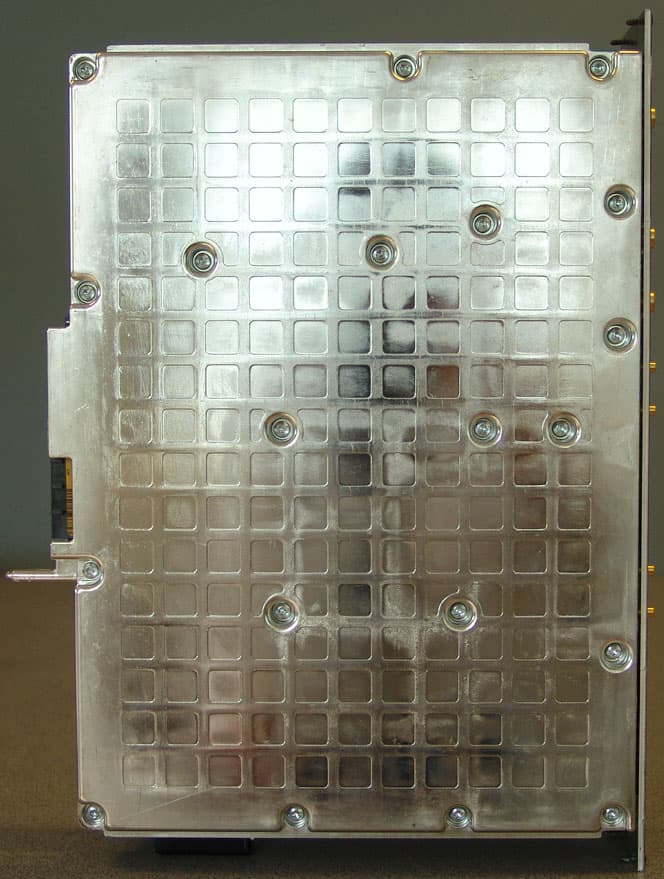
Date Page KRC 131 1010/2 R2A 2005-03-24 1(2) External photos Front side Rear side Right side Date Page KRC 131 1010/2 R2A 2005-03-24 2(2) External photos Left side
ID Label/Location Info
Date Page KRC 131 1010/2 R2A 2005-03-24 1(1) FCC ID FCC ID Label: FCC ID placement
Operational Description
Open EXHIBIT 12 1 (10) Prepared (also subject responsible if other) No. ERA/RBI/R Per Helmersson and Björn Rosenquist B5KAKRC1311010-2 Approved Checked Date Rev Reference KI/ERA/RBI/R (P Helmersson) 2005-04-05 C Exhibit 12 – Cover Sheet Contents 1 2.1033(c) Circuit Description 2 1.1 (2) FCC Identifier: B5KAKRC1311010-2 2 1.2 (4) Type of Emission: 2 1.3 (5) Frequency range. 2 1.4 (6) Range of Operating Power: 2 1.5 (7) Maximum Power Rating: 2 1.6 (8) Final Amplifier Voltage and Current in normal operation 3 1.7 (10) Frequency Stabilizing Circuit Description 3 1.8 (10) Spurious and Harmonic Suppression 3 1.9 (10) Limiting Power 3 1.10 (10) Digital Modulation 4 1.10.1 Modulation format for GMSK 4 1.10.2 Modulation format for 8PSK 7 Open EXHIBIT 12 2 (10) Prepared (also subject responsible if other) No. ERA/RBI/R Per Helmersson and Björn Rosenquist B5KAKRC1311010-2 Approved Checked Date Rev Reference KI/ERA/RBI/R (P Helmersson) 2005-04-05 C 1 2.1033(c) Circuit Description 1.1 (2) FCC Identifier: B5KAKRC1311010-2 This dTRU (double Tranceiver Radio Unit) consist of two synthesized transmitters (TRX) operating in the frequency band of 869.2 to 893.8 MHz. There are 124 Channels available with a channel spacing of 200 KHz. The transmitter is capable of operation in a TDMA (Time Division Multiple Access) system. For each channel there are 8 time slots available, each containing digital speech or data for GMSK and data for 8-PSK. The dTRU have a hybrid combiner included which can be used to increase the number of TRX:s per antenna. This combiner is connected before the cavity band pass filter in the combining system. 1.2 (4) Type of Emission: GMSK: 255KGXW 8-PSK: 254KG7W 1.3 (5) Frequency range. 869.2 to 893.8 MHz 1.4 (6) Range of Operating Power: This transmitter is designed to supply a nominal power level of 45.5 dBm at the antenna connector. The output signal from the dTRU is amplified in a separately certified MCPA and then filtered in a CDU where the antenna connector is situated. The power level can be set at 16 power levels, each with a 2 dB increment. The power levels are labeled P(0) to P(15) where P(0) is the highest power level. 1.5 (7) Maximum Power Rating: The maximum power rating with one TRX under environmental and supply voltage variations is equal to 45.5 dBm plus a power level tolerance of + 1.5 dB. Therefore the maximum peak output power is 47.0 dBm equal to 50 W at the antenna connector of the radio base station. Open EXHIBIT 12 3 (10) Prepared (also subject responsible if other) No. ERA/RBI/R Per Helmersson and Björn Rosenquist B5KAKRC1311010-2 Approved Checked Date Rev Reference KI/ERA/RBI/R (P Helmersson) 2005-04-05 C 1.6 (8) Final Amplifier Voltage and Current in normal operation Only a low power amplifier block exists. The output power to the antenna is generated in a separately certified MCPA. P (0) P (15) Drain Voltage 5 V DC 5 V DC Drain Current 80 mA DC 80 mA DC 1.7 (10) Frequency Stabilizing Circuit Description The transmitter in each TRX contains three synthesized oscillators. One PLL gives a 90 MHz signal to the I/Q modulator. The two other generate a 779 to 804 MHz signal to the mixer where the modulated signal is converted to the transmit frequency. Two oscillators are needed in frequency hopping mode, one is retuning while the other is active. All three synthesized oscillators have a reference of 13 MHz, which is mixed down by 2, generated in a central synthesized oscillator (PLL) of 26 MHz in the LTU part of the dTRU. This PLL frequency reference is extracted from the 13 MHz signal on the Y-link, which is generated and distributed, by the DXU (Distribution Switch Unit), to all dTRU:s in the base station. The frequency reference 13 MHz in the DXU is generated in a voltage controlled oscillator placed in an oven together with and phase-locked to a long-term stable oven heated oscillator. As an option the oscillator can be phase-locked to the incoming PCM-link frequency or an incoming GPS-link frequency. 1.8 (10) Spurious and Harmonic Suppression Spurious and harmonic suppression is achieved by using two separate band pass filters of ceramic type in the exciter. A filter module at the output works like a band pass filter around the carrier. In addition to these filters, the output signal passes a cavity band pass filter in the combining system. 1.9 (10) Limiting Power The TRU measures the output power at its output connector via a RF-detector and the detected value is used by the power loop control block to control two variable gain amplifiers between the modulator and the power amplifier. Open EXHIBIT 12 4 (10) Prepared (also subject responsible if other) No. ERA/RBI/R Per Helmersson and Björn Rosenquist B5KAKRC1311010-2 Approved Checked Date Rev Reference KI/ERA/RBI/R (P Helmersson) 2005-04-05 C 1.10 (10) Digital Modulation 1.10.1 Modulation format for GMSK 1.10.1.1 Modulating symbol rate The modulating symbol rate is 1/T = 1 625/6 ksymb/s (i.e. approximately 270.833 ksymb/s), which corresponds to 1 625/6 kbit/s (i.e. 270.833 kbit/s). T is the symbol period. 1.10.1.2 Start and stop of the burst Before the first bit of the bursts as defined in GSM 05.02 [3] enters the modulator, the modulator has an internal state as if a modulating bit stream consisting of consecutive ones (d i = 1) had entered the differential encoder. Also after the last bit of the time slot, the modulator has an internal state as if a modulating bit stream consisting of consecutive ones (d i = 1) had continued to enter the differential encoder. These bits are called dummy bits and define the start and the stop of the active and the useful part of the burst as illustrated in figure 1. Nothing is specified about the actual phase of the modulator output signal outside the useful part of the burst. dummy bits Output phase The useful part The active part 000..............000 111111..............111111 3 tail bits3 tail bitsdummy bits 1/2 bit1/2 bit Figure 1: Relation between active part of burst, ta…
Text truncated - open the document above for the full version.
Parts List/Tune Up Info
Open EXHIBIT 10 1 (15) Prepared (also subject responsible if other) No. EAB/RBI/R Per Helmersson B5KAKRC1311010-2 Approved Checked Date Rev Reference KI/EAB/RBI/R (P Helmersson) 2005-03-22 A Exhibit 10 - Components, Tune Up Contents 1 2.1033 (c) (10) Function of Active Circuit Devices..............................2 1.1 Printed Board TBU 800 MHz GMSK/8-PSK ROA 128 1360/2............2 1.1.1 Function Block CPU............................................................................2 1.1.2 Function Block Sparc 1.......................................................................3 1.1.3 Function Block Sparc 2.......................................................................4 1.1.4 Function Block DC/DC........................................................................5 1.1.5 Function Block LTU.............................................................................6 1.1.6 Function Block RX IF1.........................................................................7 1.1.7 Function Block RX IF2.........................................................................8 1.1.8 Function Block Front end....................................................................9 1.1.9 Function Block TX1 800....................................................................11 1.1.10 Function Block TX2 800....................................................................12 1.2 Function Block Back end 800............................................................13 2 2.1033(c)(9) Tune-Up Procedure......................................................14 3 2.1033(c)(9,10) Power Tune-Up – Power Limiting............................15 Open EXHIBIT 10 2 (15) Prepared (also subject responsible if other) No. EAB/RBI/R Per Helmersson B5KAKRC1311010-2 Approved Checked Date Rev Reference KI/EAB/RBI/R (P Helmersson) 2005-03-22 A 1 2.1033 (c) (10) Function of Active Circuit Devices 1.1 Printed Board TBU 800 MHz GMSK/8-PSK ROA 128 1360/2 1.1.1 Function Block CPU ROZ 104 410/1 Revision B Pos Prod name/Func des Product number Z3001 MICROCIRCUIT/74'08 LVC TSSOP14 4x 2-INP AND RYT 331 0008/3C Z3100 PROD. ADAPT. CIRCUIT/ASIC POWER GARP ROP 101 1192/1 Z3303 MICROCIRCUIT/74'14 LVC TSSOP14 6x INVERT SC RYT 331 0014/3C Z3400 MICROCIRCUIT/SDRAM 16M16 133MHz CL=3 100MHz RYT 119 6142/5 Z3401 MICROCIRCUIT/SDRAM 16M16 133MHz CL=3 100MHz RYT 119 6142/5 Z3402 MICROCIRCUIT/74'08 LVC1G SC70-5 1x 2-INP D- RYT 326 6008/52C Z3403 MICROCIRCUIT/FLASH TB 2M16 90NS 3.3V I RYT 118 6152/6 Z3404 MICROCIRCUIT/FLASH 8M16 150NS 3.3V E RYT 118 6153/1 Z3601 MICROCIRCUIT/LVDS LINE DRIVER x4 TSSOP16 /9 RYT 109 6181/2C Z3602 MICROCIRCUIT/LVDS LINE RECEIVER x4 TSSOP16 RYT 109 6158/2C Z3603 MICROCIRCUIT/RS485/RS422 TRANSCEIVER x1 3.3 RYT 109 6243/3 Z3604 MICROCIRCUIT/RS485/RS422 TRANSCEIVER x1 3.3 RYT 109 6243/3 Z3605 MICROCIRCUIT/RS485/RS422 TRANSCEIVER x1 3.3 RYT 109 6243/3 Z3606 MICROCIRCUIT/RS485/RS422 TRANSCEIVER x1 3.3 RYT 109 6243/3 Z3607 FUNCTIONAL COMPONENT/CDU MUX PLD RON 107 496 Z3700 MICROCIRCUIT/74'244 LVC SSOP20 8x BUFFER NO RYT 331 0244/C Z3701 MICROCIRCUIT/74'244 LVC SSOP20 8x BUFFER NO RYT 331 0244/C Z3702 MICROCIRCUIT/74'244 LVC SSOP20 8x BUFFER NO RYT 331 0244/C Open EXHIBIT 10 3 (15) Prepared (also subject responsible if other) No. EAB/RBI/R Per Helmersson B5KAKRC1311010-2 Approved Checked Date Rev Reference KI/EAB/RBI/R (P Helmersson) 2005-03-22 A 1.1.2 Function Block Sparc 1 ROZ 104 404/2 Revision A Pos Prod name/Func des Product number L5200 FILTER/50ohm 1206 3A 0.025ohm Bead REG 706 21/1 L5201 FILTER/50ohm 1206 3A 0.025ohm Bead REG 706 21/1 L5300 FILTER/50ohm 1206 3A 0.025ohm Bead REG 706 21/1 L5301 FILTER/50ohm 1206 3A 0.025ohm Bead REG 706 21/1 Z5000 MICROCIRCUIT/74'08 LVC TSSOP14 4x 2-INP AND RYT 331 0008/3C Z5001 MICROCIRCUIT/FLASH SPI 128K8 20MHz 2.7V I RYT 118 6154/2 Z5002 MICROCIRCUIT/74'86 LVC,Z1G SC70-5 1x 2-INP RYT 326 6086/42C Z5003 MICROCIRCUIT/74'08 LVC1G SC70-5 1x 2-INP D- RYT 326 6008/52C Z5200 PROD. ADAPT. CIRCUIT/EDGE BASE BAND ASIC, EBBA ROP 101 1189/1 Z5201 MICROCIRCUIT/SDRAM 16M16 133MHz CL=3 100MHz RYT 119 6142/5 Z5300 PROD. ADAPT. CIRCUIT/TARAC_U+ ROP 101 1128/2 Open EXHIBIT 10 4 (15) Prepared (also subject responsible if other) No. EAB/RBI/R Per Helmersson B5KAKRC1311010-2 Approved Checked Date Rev Reference KI/EAB/RBI/R (P Helmersson) 2005-03-22 A 1.1.3 Function Block Sparc 2 ROZ 104 405/2 Revision A Pos Prod name/Func des Product number L6200 FILTER/50ohm 1206 3A 0.025ohm Bead REG 706 21/1 L6201 FILTER/50ohm 1206 3A 0.025ohm Bead REG 706 21/1 L6300 FILTER/50ohm 1206 3A 0.025ohm Bead REG 706 21/1 L6301 FILTER/50ohm 1206 3A 0.025ohm Bead REG 706 21/1 Z6000 MICROCIRCUIT/74'08 LVC TSSOP14 4x 2-INP AND RYT 331 0008/3C Z6001 MICROCIRCUIT/74'86 LVC,Z1G SC70-5 1x 2-INP RYT 326 6086/42C Z6002 MICROCIRCUIT/74'08 LVC1G SC70-5 1x 2-INP D- RYT 326 6008/52C Z6200 PROD. ADAPT. CIRCUIT/EDGE BASE BAND ASIC, EBBA ROP 101 1189/1 Z6201 MICROCIRCUIT/SDRAM 16M16 133MHz CL=3 100MHz RYT 119 6142/5 Z6300 PROD. ADAPT. CIRCUIT/TARAC_U+ ROP 101 1128/2 Z6301 MICROCIRCUIT/FLASH SPI 128K8 20MHz 2.7V I RYT 118 6154/2 Open EXHIBIT 10 5 (15) Prepared (also subject responsible if other) No. EAB/RBI/R Per Helmersson B5KAKRC1311010-2 Approved Checked Date Rev Reference KI/EAB/RBI/R (P Helmersson) 2005-03-22 A 1.1.4 Function Block DC/DC ROZ 104 406/1 Revision A Pos Prod name/Func des Product number D701 DIODE/SWI x2 70V 200mA SOT23 serial RKZ 123 03/1 D702 DIODE/SWI x2 70V 200mA SOT23 com.cat RKZ 123 03/3 D704 DIODE/SWI x2 70V 200mA SOT23 serial RKZ 123 03/1 D705 DIODE/SWI x2 70V 200mA SOT23 serial RKZ 123 03/1 D706 MICROCIRCUIT/MOSFET DRIVERx2 INV/NONINV /44 RYT 109 6204/1 D707 MICROCIRCUIT/MOSFET DRIVERx2 INV/NONINV /44 RYT 109 6204/1 D708 RECTIFIER/REC 200V 1A SMA 35ns RKZ 123 05/2 D709 RECTIFIER/REC 200V 1A SMA 35ns RKZ 123 05/2 D711 DIODE/REC SCH 40V 2A SMB 0.44V(2A) RKZ 323 487/2 D712 DIODE/REC SCH 40V 2A SMB 0.44V(2A) RKZ 323 487/2 D713 DIODE/SWI SCH x2 40V 120mA SOT23 ser RKZ 323 17/1 N700 MICROCIRCUIT/2 Chan Sync Curre…
Text truncated - open the document above for the full version.
Test Report
Date Reference Page REPORT 2005-04-04 F504182-F22 1 (4) FCC ID: B5KAKRC1311010-2 Appendix 1 Description - Equipment Under Test (EUT) Equipment: GSM Base station transceiver 800 MHz Tx Frequency range: 869.2-893.8 MHz Nominal power voltage: 24 V DC Tested Channels All tests were performed with the EUT operating together with power amplifier, MCPA KRB 111 102/1 Rev R1B with FCC ID: E675JS0071. Radiated measurements: RF configuration 1x4 dTRU ARFCN Frequency Modulation 128 869.2 MHz GMSK No 1 169 877.4 MHz 8-PSK 210 885.6 MHz GMSK No 2 251 893.8 MHz 8-PSK RF configuration 1x8 dTRU ARFCN Frequency Modulation 128 869.2 MHz GMSK No 1 146 872.8 MHz 8-PSK 164 876.4 MHz GMSK No 2 182 880.0 MHz 8-PSK 197 883.0 MHz GMSK No 3 215 886.6 MHz 8-PSK 233 890.2 MHz GMSK No 4 251 893.8 MHz 8-PSK RF configuration 1x12 dTRU ARFCN Frequency Modulation 128 869.2 MHz GMSK No 1 139 871.4 MHz 8-PSK 150 873.6 MHz GMSK No 2 161 875.8. MHz 8-PSK 172 878.0 MHz GMSK No 3 183 880.2 MHz 8-PSK 196 882.8 MHz GMSK No 4 207 885.0 MHz 8-PSK 218 887.2 MHz GMSK No 5 229 889.4 MHz 8-PSK 240 891.6 MHz GMSK No 6 251 893.8 MHz 8-PSK Note : For configuration 1x12 the maximum output power was limited to 2 dB below maximum output power. The radiated spurious emission measurements were done with the three RF configurations listed above at the same time to simulate worst case. All radiated measurements were performed with the EUT installed in a RBS 2250 TRX cabinet powered with DC power. The RBS 2250 is a dual band cabinet. During the test the RBS 2250 was also equipped with 1900 MHz transceivers and activated to simulate worst case scenario. Date Reference Page REPORT 2005-04-04 F504182-F22 2 (4) FCC ID: B5KAKRC1311010-2 Appendix 1 Conducted measurements: ARFCN Frequency 128 869.2 MHz 129 869.4 MHz 153 874.2 MHz 190 881.6 MHz 226 888.8 MHz 250 893.6 MHz 251 893.8 MHz All RF conducted measurements were performed with the EUT installed in a RBS 2250 TRX cabinet powered with DC power. The measurements were done at the output connector of CDU-L8 (BFL 119 437/1 rev. R1B) with serial number A400154972. The dTRU with serial number AE51645885 was used for the measurements. The measurement was performed with configurations that represents worst case scenario. Manufacturer’s representative Per Helmersson, Ericsson AB Purpose of test The purpose of the tests is to verify compliance to the performance characteristics specified in FCC CFR47. References Measurements were done according to relevant parts of the following standards: ANSI/TIA/EIA-603-B-2002 J-STD007A Vol 1 ANSI/TIA/EIA 136-280-B-2000 Reservation The test results in this report apply only to the particular Equipment Under Test (EUT) as declared in the report. Delivery of test object The test object was delivered: 2005-02-28 Test engineers Reinhold Reul, Peter Grahn, and Jonas Bremholt Test witnesses Lars Hagbjörk, Ericsson AB Date Reference Page REPORT 2005-04-04 F504182-F22 3 (4) FCC ID: B5KAKRC1311010-2 Appendix 1 Test set-up, conducted measurements 1. Computer, with software RBSMMI ver. R9A02 2. Ericsson RBS Master 2 LPY 107 1007/1 software ver. R4C01 Date Reference Page REPORT 2005-04-04 F504182-F22 4 (4) FCC ID: B5KAKRC1311010-2 Appendix 1 Test set-up, radiated measurements 1. 3 units, Computers, with software RBSMMI ver. R9A02 2. 3 units, Ericsson RBS Master 2 LPY 107 1007/1 software ver. R4C01 3. 6 units, Dummy loads (50 ohm) Interfaces: Type of port: 24 VDC DC power Antenna: Coaxial cable (50 ohm) Antenna G703: T1, shielded multi-wire (120 ohm) Telecom TG-sync: Shielded multi-wire Signal Alarm: Unshielded 4 wire Signal GPS: Shielded multiwire Signal Date Reference Page REPORT 2005-04-04 F504182-F22 1 (1) FCC ID: B5KAKRC1311010-2 Appendix 2 RF Power output measurements according to 47CFR 2.1046 Date 2005-03-07 Temperature 22 °C ± 3 °C Humidity 20 % ± 5 % Test set-up and procedure Measurements were made at CDU-L8 output connector. The output was connected to a Peak power analyser via a 50 ohm attenuator. The transmitter was modulated with pseudorandom data and with maximum power in all the time slots during the measurements. Measurement equipment Calibration Due SP number Boonton RF Peak power meter/analyzer 2005-03 503 144 Boonton Power sensor 56518-S/4 2005-03 503 145 Multimeter Fluke 87 2005-11 502 190 Testo 610, Temperature and humidity meter 2006-12 502 658 Measurement uncertainty: 0.5 dB Results GMSK Rated output power level after CDU-L8 (maximum): 45.5 dBm Test conditions Transmitter power (dBm) Peak/ Average T nom 22 °C/ V nom 24 V DC Channel 128 Channel 190 Channel 251 TRX 1: 45.7/ 45.0 45.5/ 44.8 45.0/ 44.2 TRX 2: 45.5/ 44.7 45.4/ 44.7 44.7/ 44.0 8-PSK Rated output power level after CDU-L8 (maximum): 45.5 dBm Test conditions Transmitter power (dBm) Peak/ Average T nom 22 °C/ V nom 24 V DC Channel 128 Channel 190 Channel 251 TRX 1: 45.8/ 41.9 45.7/ 41.8 45.0/ 41.1 TRX 2: 45.4/ 41.6 45.4/ 41.5 44.7/ 40.9 Limit GMSK: The measured output power shall be within ± 2dB of the rated output power (J-STD007A Vol 1) 8-PSK: The measured output power shall be within +1 to -3 dB of the rated output power (ANSI/TIA/EIA 136-280-B) Complies? Yes Date Reference Page REPORT 2005-04-04 F504182-F22 1 (1) FCC ID: B5KAKRC1311010-2 Appendix 3 Modulation characteristics measurements according to 47CFR 2.1047 Date 2005-03-02 Temperature 21 °C ± 3 °C Humidity 22 % ± 5 % Test set-up and procedure Measurements were made at CDU-L8 output connector. The output was connected to a spectrum analyser. The spectrum analyser was connected to an external 10 MHz reference standard during measurement. The transmitter was activated at maximum output power and modulated with pseudorandom data during the measurements. Measurement equipment Calibration Due SP number R&S FSIQ 2005-04 503 738 Multimeter Fluke 87 2005-11 502 190 Testo 610, Temperature and humidity meter 2006-12 502 658 Results Tested channel: 190 (881.6 MHz) GMSK Test conditions Phase error (° RMS ) Supply voltage DC (V) T (°C) TRX 1 TRX 2 24.0 +20 0…
Text truncated - open the document above for the full version.
Contact Information
Applicant
Bo Bergstrom(Manager)
+468 757 0401Fax: +468 751 4687
Technical Contact
Test Firm
SP Technical Research Institute of SwedenMagnus Winehem
Technical Specifications
| # | Rule Parts | Frequency Range | Power Output | Emission | Tolerance |
|---|---|---|---|---|---|
| 2 | 22H | 869.2 MHz - 893.8 MHz | 35.5 W | 254KG7W | 0.05 ppm |
Other Applications from Ericsson Radio Systems AB
B5KEKRC1311004-2
Jun 13, 2007PCS Broadband GSM Base station transceiver
Equipment Class
PCB - PCS Licensed Transmitter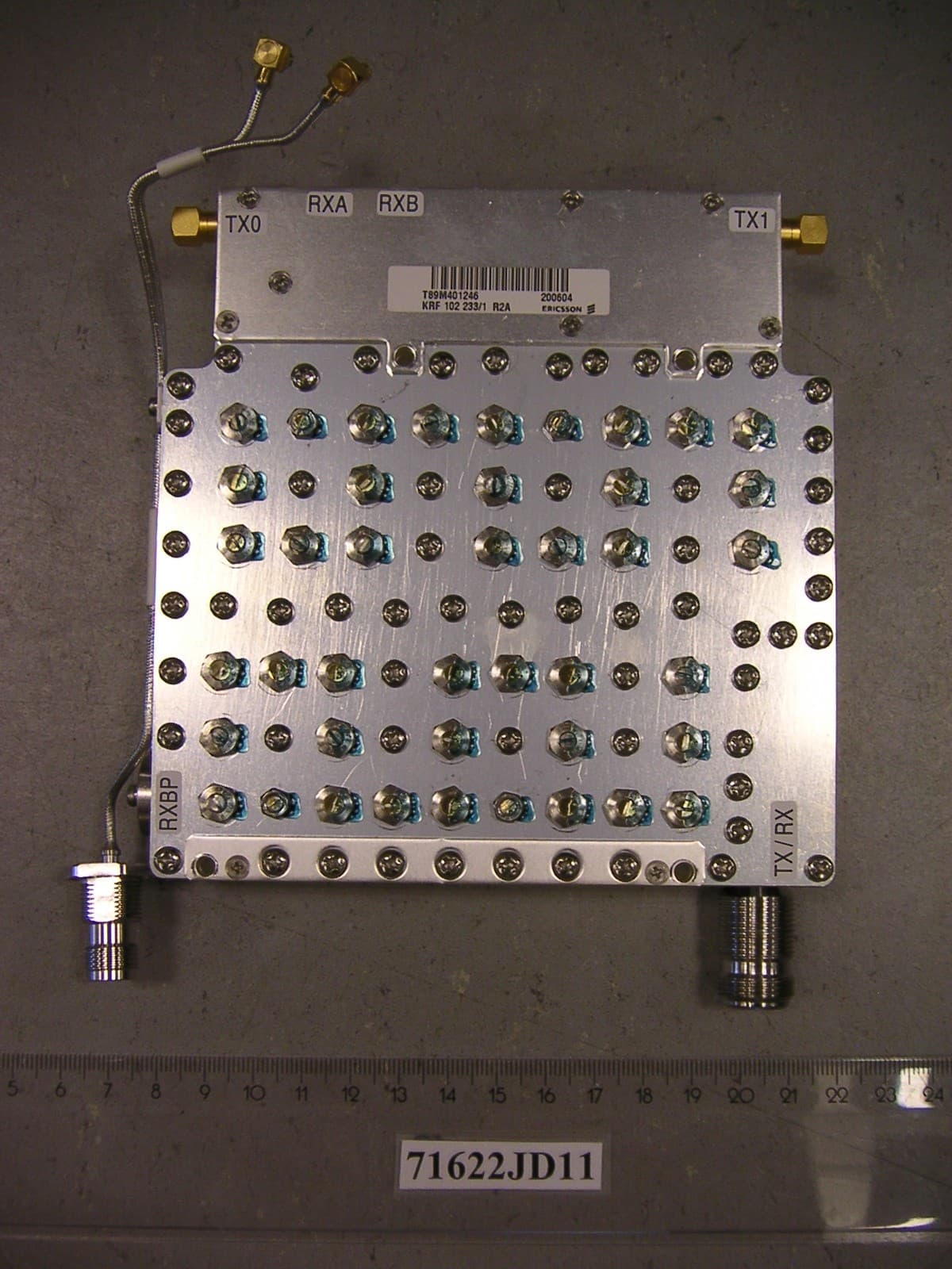
B5KCKRC16184-3
Sep 26, 2006PCS Broadband GSM Base station
Equipment Class
PCB - PCS Licensed Transmitter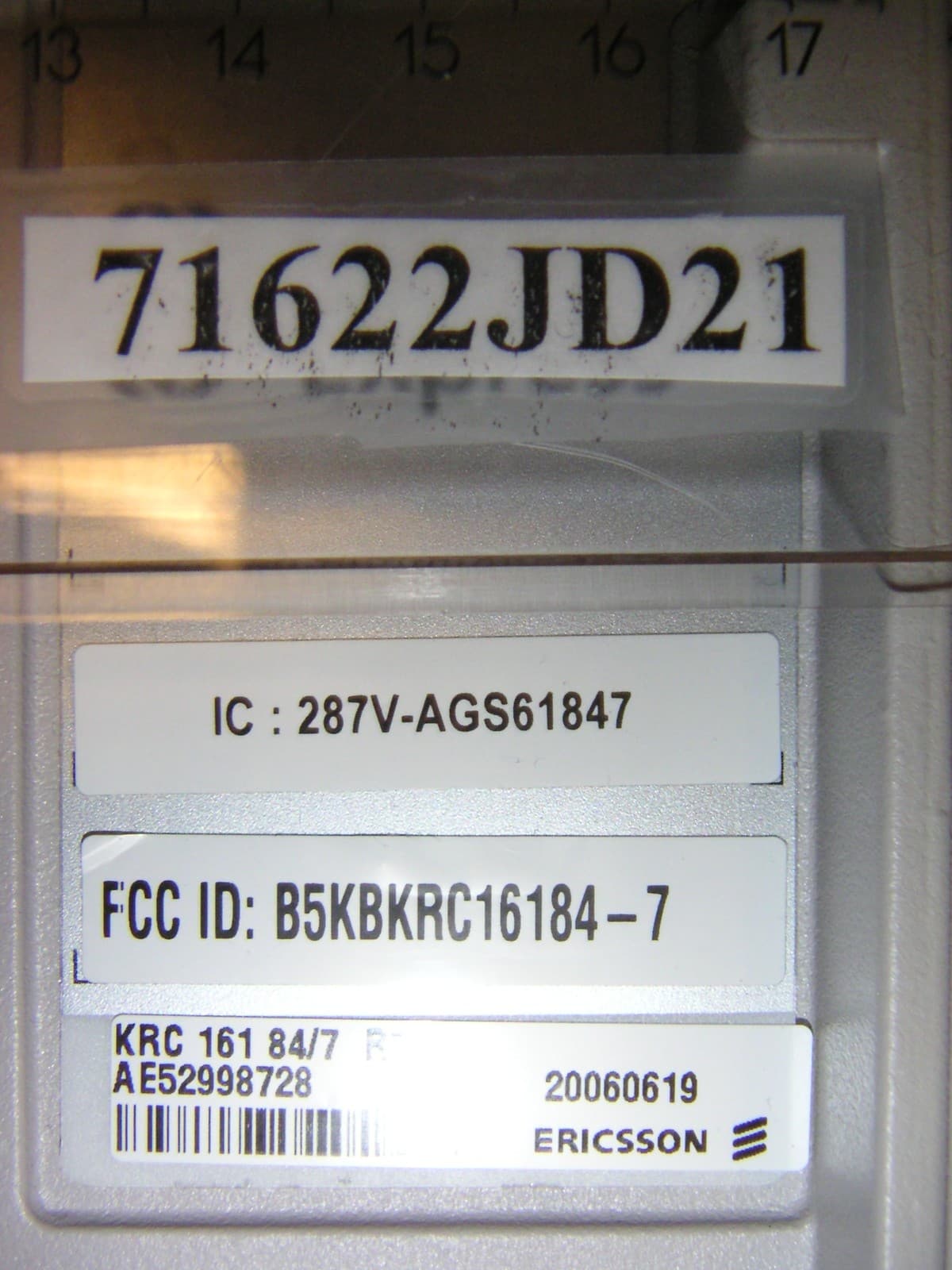
B5KCKRC16184-7
Sep 26, 2006PCS Broadband GSM Base station
Equipment Class
TNB - Licensed Non-Broadcast Station Transmitter
B5KDKRC1311005-2
Sep 06, 2006Broadband GSM Base station transceiver
Equipment Class
TNB - Licensed Non-Broadcast Station Transmitter
B5KAKRC1311013-2
Apr 04, 2005Broadband GSM Base station transceiver
Equipment Class
PCB - PCS Licensed Transmitter