B5KAKRC161028-1PCS Broadband GSM Base Station
Ericsson Radio Systems AB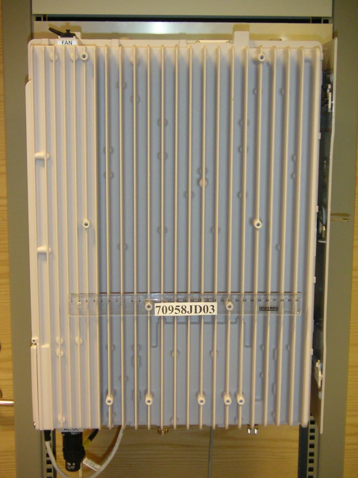
Click to zoom
Application Details
- Equipment Class
- TNB - Licensed Non-Broadcast Station Transmitter
- Date of Grant
- Mar 08, 2005
- Application Purpose
- Original Equipment
- Date of Application
- Mar 08, 2005
- Equipment Note
- PCS Broadband GSM Base Station
- Frequency Range
- 869.20000000 - 893.80000000
- Company
- Ericsson Radio Systems AB
- Country
- Sweden
Documents & Files
Document Text
Text extracted from the exhibit documents filed with the FCC. Open a document above to read the original.
Users Manual
P012346A EN/LZT 720 0090 R1A Ericsson GSM System RBS 2109 User’s Guide Doc nr: 2/001 59-EN/LZT 720 0090 Uen Rev A Ericsson GSM System EN/LZT 720 0090 R1A RBS 2109 User’s Guide BINDER LABEL 1 (1) Uppgjord (även faktaansvarig om annan) - Prepared (also subject responsible if other) Nr - No. KI/EAB/RWB/Z Fredrik Hammar 4/001 59-EN/LZT 720 0090 Uen Dokansv/Godkänd - Doc respons/Approved Kontr - Checked Datum - Date Rev File KI/EAB/RWB/Z Sun ita Patil 20 04-09 -17 A http://sis/documents/word/binderlabel_portrait.doc 98 65 Fontsize 10 Fontsize 10 HEADING XXX LZN xxx xxx R-state 28 38 47 54 RBS 2109 User’s Guide Ericsson GSM System EN/LZT 720 0090 R1A Fontsize 12 Cutting mark Fontsize 14 CAPTION LIST Document No. EN/LZT 720 0090 RBS 2109 User’s Guide Date Rev 2004-09-17 A Introduction 1 Personal Health and Safety Information 2 System Safety Information 3 Tools and Instruments 4 Installation of RBS 2308 and RBS 2309 5 Antenna System Tests 6 Site Installation Tests 7 RBS Site Integration 8 Maintenance 9 Glossary 10 RBS 2109 User’s Guide E Copyright © Ericsson 2004 — All Rights Reserved Disclaimer No part of this document may be reproduced in any form withoutthe written permission of the copyright owner. The contents of this document are subject to revision without notice due to continued progress in methodology, design and manufacturing. Ericsson shall have no liability for any error or damage of any kind resulting from the use of this document. Trademark List EN/LZT 720 0090 Uen R1A 2004-09-17 RBS 2109 User’s Guide Contents 1Introduction1 1.1Product Overview2 1.2Target Groups3 1.3Installation and Integration Process Overview4 1.4Radio Site Implementation Process5 1.5RBS Library Overview8 1.6Release History8 2Personal Health and Safety Information9 2.1Introduction9 2.2Hazard Symbols and Admonitions10 2.3General Safety Precautions11 2.4Electric Shock Hazards12 2.5Energy Hazards13 2.6Fire Hazard14 2.7Heat Hazards15 2.8Mechanical Hazards16 2.9Radio Frequency Exposure Hazards17 2.10Laser Hazards18 2.11Chemical Hazards19 2.12Other Hazards21 3System Safety Information25 3.1Introduction25 3.2Admonitions and Safety Symbols26 3.3Batteries27 3.4Electrical Installation28 3.5Electrostatic Discharge29 3.6Equipment Handling30 3.7Ground Connection31 3.8Lightning Protection31 4Tools and Instruments33 4.1Tools for Installation of RBS 210933 EN/LZT 720 0090 Uen R1A 2004-09-17 RBS 2109 User’s Guide 4.2Equipment for Antenna System Tests34 4.3Equipment for Site Installation Tests35 4.4Equipment for RBS Site Integration35 4.5Equipment for Maintenance36 4.6Kit Specifications37 5Installation of RBS39 5.1Introduction39 5.2Preconditions39 5.3Torque Settings40 5.4Installation Procedure41 6Antenna System Tests73 6.1Checking the Installation76 6.2Calibrating the Antenna Tester76 6.3Performing DTF Tests79 6.4Naming a DTF Measurement83 6.5Calculating the Feeder Attenuation84 6.6Calculating the Feeder Delay86 6.7Performing SWR Test on Passive Antenna Systems (Without TMA)89 6.8Performing SWR Test on Antenna Systems with ddTMA91 6.9Naming an SWR Measurement95 6.10Performing Concluding Routines95 6.11SWR↔Return Loss Conversion Table98 7Site Installation Tests101 7.1Preconditions101 7.2Inspecting Cable Connections102 7.3Checking AC Mains and DC Power Supply102 7.4Switching on RBS103 7.5Testing Fan Unit105 7.6Setting IDB Parameters106 7.7Reading Fault Status135 7.8Testing External Alarms136 7.9Performing Concluding Routines138 8RBS Site Integration143 8.1Testing Transmission144 EN/LZT 720 0090 Uen R1A 2004-09-17 RBS 2109 User’s Guide 8.2Bringing the RBS into Service146 8.3Making Test Calls on the Air Interface147 8.4Performing Concluding Routines151 9Maintenance157 9.1Introduction157 9.2Preconditions157 9.3Fault Localisation Using OMT158 9.4Troubleshooting Using the RBS Indicators175 9.5HW Replacement187 10Glossary221 EN/LZT 720 0090 Uen R1A 2004-09-17 RBS 2109 User’s Guide EN/LZT 720 0090 Uen R1A 2004-09-17 RBS 2109 User’s Guide 1Introduction This User’s Guide consists of the chapters listed below. Each chapter is briefly summarised. Introduction This chapter. Personal Health and Safety Information Contains personal health and safety information that applies when working with Ericsson system products. System Safety Information Contains system safety information that applies when working with Ericsson system products. Tools and Instruments Contains lists of all recommended tools and instruments. Installation of the RBS Describes activities for: • Installation of the mounting base • Connection of cables • Connection of external antenna • Mounting the radio cabinet on the mounting base Antenna System Tests Describes the site specific antenna tests that should be performed on site. Site Installation Tests Describes the site specific tests that should be performed on-site. 1EN/LZT 720 0090 Uen R1A 2004-09-17 RBS 2109 User’s Guide RBS Site Integration Describes how to integrate an RBS site into a network. Maintenance Describes first line Maintenance. This means that swap repair is carried out on site and that only replaceable units are handled. Glossary Contains abbreviations and acronyms used in the text. 1.1Product Overview The RBS is a GSM EDGE micro base station for both indoor and outdoor micro cell applications. It is a small yet complete station, with transceivers, switching functions and transmission. The RBS can be mounted on a mast/pole as easily as it can be fitted to a wall. P010530D Figure 1RBS Overview 2E N/LZT 720 0090 Uen R1A 2004-09-17 RBS 2109 User’s Guide IXUInterface and Switching Unit MBUMounting Base Unit RRURemote Radio Unit RXBPRX Bandpass Filter TIMTransmission Interface Mod ule External optional battery backup is possible, as well as theoption of having integrated antennas within the base station. 1.2Target Groups This section describes the target group for this manual, which is all personnel involved in activities relating to the installation and integration of an RBS site. TEMS ON/OFF YES NO 1 2 3 4 5 6 7 8 9…
Text truncated - open the document above for the full version.
Users Manual
RBS 2109 User’s Guide Example of an Unacceptable DTF Measurement P007952A CAL ON LIM ON 259 POINTS RECALL 1.20 ON/OFF 50.0DIST (m)0.0 1.00 EDIT DELTA (M2 - M1) MARKER TO PEAK BACK M3=OFFM1:1.01,2.3m M4=OFF :+0.07, +38.6m DTF DTF2 MARKER TO VALLEY 2 Figure 36Example of an Unacceptable DTF Measurement 6.3.3Measuring Feeder Length This section describes how to measure the feeder length, based on the result of the test in chapter Section 6.3.2 Testing Feeder Installation on page 80. 1. Press theMARKERkey. 2. Press theM1soft key. 3. Press theEDITsoft key and place the M1 marker at the near end of the feeder using theUP/DOWN arrowkey.See figure below. 8 2 E N/LZT 720 0090 Uen R1A 2004-09-17 RBS 2109 User’s Guide P007951A CAL ON LIM ON 259 POINTS RECALL 1.20 ON/OFF 50.0DIST (m) 0.0 1.00 EDIT DELTA (M2 - M1) MARKER TO PEAK BACK M3=OFF M4=OFF DTF DTF1 MARKER TO VALLEY M1:1.01,2.3m :+0.07, +38.6m 2 Figure 37Placing the M1 and M2 Markers 4. Press theBACKsoft key and then theM2soft key. 5. Press theEDITsoft key and place the M2 marker at the far end of the feeder, using theUP/DOWN arrowkey.See figure above. 6. Press theDELTA (M2–M1)soft key and enter the 2 value as the feeder length in the test record. 7. Create a unique trace name according toSection 6.4 Naming a DTF Measurement on page 83. Save the measurement by pressing theSAVE DISPLAYkey. Type in the trace name using the alphanumeric soft keys, and pressENTER. 6.4Naming a DTF Measurement This section describes how to give the measurement a unique name that is traceable to a specific antenna system on a specific site. 1. Find the cell ID in theSite Installation Documentation. 2. Read the label text on the jumper being measured. 3. Combine the measurement type, cell ID and label text (a unique name with a maximum of 16 characters). The following example illustrates these steps: 83EN/LZT 720 0090 Uen R1A 2004-09-17 RBS 2109 User’s Guide 1. The cell ID found in theSite Installation Documentationis "SOF007_A". 2. The text on the feeder label is "Cell A: DX1". 3. The type of measurement is DTF, so the name of the measurement is "DTFSOF007ADX1". Example 1Naming a DTF Measurement 6.5Calculating the Feeder Attenuation This section describes how to calculate the attenuation of the feeder system. 1. Use the feeder length measured inSection 6.3.3 Measuring Feeder Length on page 82. 2. Find the attenuation value (dB/m) for the cable type in thetable below. Calculate the total attenuation for each feeder and jumper,by multiplying the length in metres by the attenuation per metre. 3. Add the attenuations for the feeder and the jumpers,see Table 15 on page 85 4. Enter the result of the calculation in the test record. 5. Repeat the DTF test, and calculate the feeder attenuationfor all antenna feeders on the site. 8 4 E N/LZT 720 0090 Uen R1A 2004-09-17 RBS 2109 User’s Guide Table 15Attenuation for Different Cables Attenuation, dB/m (CABLE LOSS) Feeder Type Andrew GSM 800GSM 1900 1/4” LDF1 0.1240.195 1/4” FSJ1 (flex) 0.1790.278 3/8” LDF2 0.1060.166 3/8” FSJ2 (flex) 0.1210.191 1/2” LDF4 0.0660.104 1/2” FSJ4 (flex) 0.1070.171 7/8” LDF5 0.0370.060 1 1/4” LDF6 0.0270.043 1 5/8” LDF7 0.0220.036 Note:If the cable type is not found in the table above, then the values must be taken from the manufacturer’s specifications. Example of Calculating the Total Feeder Attenuation (GSM 1900) Test Record P007920A A B C A + B + C = Total Feeder Attenuation Figure 38Example of Calculating the Total Feeder Attenuation 85EN/LZT 720 0090 Uen R1A 2004-09-17 RBS 2109 User’s Guide Example 2Calculating the Total Feeder Attenuation 6.6Calculating the Feeder Delay This section describes how to calculate the total delay in the feeder system. 1. Use the feeder length measured inSection 6.3.3 Measuring Feeder Length on page 82. 2. Find the delay value (ns/m) for the cable type inTable 15 on page 85. Calculate the total attenuation for each feeder and jumper,by multiplying the length in metres with the delay per metre. 3. Add the delay for the feeder and the jumpers. 4. Enter the result of the calculation in the test record. 5. Calculate the feeder delay for all antenna feeders. 8 6 E N/LZT 720 0090 Uen R1A 2004-09-17 RBS 2109 User’s Guide Table 16Delay Specifications for Different Cables Feeder Type AndrewDelay, ns/m 1/4” LDF1 3.9 1/4” FSJ1 (flex) 4.0 3/8” LDF2 3.8 3/8” FSJ2 (flex) 4.0 1/2” LDF4 3.8 1/2” FSJ4 (flex) 4.1 7/8” LDF5 3.7 1 1/4” LDF6 3.7 1 5/8” LDF7 3.8 Note:If the cable type is not found in the table above, the values must be taken from the manufacturer’s specifications. 87EN/LZT 720 0090 Uen R1A 2004-09-17 RBS 2109 User’s Guide Example of Calculating the Total Feeder Delay Example 3Calculating the Total Feeder Delay 8 8 E N/LZT 720 0090 Uen R1A 2004-09-17 RBS 2109 User’s Guide 6.7Performing SWR Test on Passive Antenna Systems (Without TMA) The purpose of the SWR test is to verify that the antenna system functions correctly when it is completely installed. The test verifies that the SWR is not too high and that the signal is not reflected back into the RBS. 6.7.1Connecting SWR Test Setup This section describes how to connect the SWR test setup for passive antenna systems (without TMA). 1. Connect the test equipment to the RBS jumper, see figure below. 2. Check that all connections are properly connected and tightened. P010263A Feeder Antenna Jumper Antenna Test Equipment RBS Jumper Figure 39Test Setup for Passive Antenna Systems (No TMA) 6.7.2Testing the Antenna System 1. Check that the Site Master’s display shows ‘‘CAL ON’’, indicating that the Site Master is calibrated. If the display shows ‘‘CAL OFF’’,calibrate the Site Master according toSection 6.2 Calibrating the Antenna Tester on page 76. 2. Ensure that the test equipment is connected according toSection 6.7.1 Connecting SWR Test Setup on page 89. 3. Press theAMPLITUDEkey to set the scale. 4. Press theTOPsoft key, enter 2.0 , and pressENTER. 5. Press theLIMIT EDITsoft key, enter 1.4 , and pressENTER. Note:Ensure that Limit …
Text truncated - open the document above for the full version.
Block Diagram
Limited Internal EXHIBIT 4 Prepared (also subject responsible if other) No. EAB/RTL/I Palle Zetterstrand B5KAKRC161028-1 Approved Checked Date Rev Reference EAB/RTL/I (P. Zetterstrand) 2005-02-16 A 1 EXHIBIT 4 - Cover Sheet Contents EXHIBIT 4 - Cover Sheet 1 Block Diagram RF Parts, RAB 800 , 1911-ROA 219 5747/1 2 Block Diagram CPU Parts, DRB, 1911-ROA 117 4767/3 3 Sheet 4 5 6 7 8 9 10 11 12 13 14 15 16 A B C D E F G H I J K Prepared (also subject responsible if other) References Doc respons/Approved Date Rev Product name Document no A B C D E F G H 1234567891011 I J K 12 13 14 15 16 123 RX_FRONTEND REF_RANGE_5100 ROZ 104 348/1 RX FRONTEND ROZ 104 383/1 REF_RANGE_7100 RX1 ROZ 104 350/1TXPA1 REF_RANGE_9100 TXPA1 ROZ 104 349/1TXPA0 REF_RANGE_8100 TXPA0 ROZ 104 382/1 REF_RANGE_6100 RX0 1911-ROA 219 5747/1 Ux 2004-09-15 EMWCOEM EMWHELN PA1MGC BS C.2 EAB/RTL/R (Anders Lindahl) RAB-H8 1(1) +7V +5.7V +26V +3.3V +5.7V +7V +1.8V +26V +5.7V +7V +26V +5.7V +3.3V +5.7V +7V +3.3V +3.3V +7V RX1_RFIC_13MHZ RXIF1_13MHZ PBU1_CTRL_BUS(8:0) TX1_CTRL_BUS(15:0) RX1_J1_BUS(18:0) SPIRA1_BUS(27:0) SPIRA1_TXQ_BUS(11:0) SPIRA1_TXI_BUS(11:0) RX0_ARF RX0_BRF RX1_ARF RX1_BRF RX0_J1_BUS(18:0) PBU0_CTRL_BUS(8:0) SPIRA0_BUS(27:0) SPIRA0_TXI_BUS(11:0) SPIRA0_TXQ_BUS(11:0) TX0_CTRL_BUS(15:0) RX1_TEMP +3.3V +5.7V RX0_J3_BUS(8:0) RX0_RFIC_13MHZ RX0_RFIC_13MHZ RX0_TEMP RXIF0_13MHZ RC0_PA_ON RF_LOOP_0 RC1_PA_ON RF_LOOP_1 TX1_RFIC_13MHZ RX1_J3_BUS(8:0) Sheet 4 5 6 7 8 9 10 11 12 13 14 15 16 A B C D E F G H I J K Prepared (also subject responsible if other) References Doc respons/Approved Date Rev Product name Document no A B C D E F G H 1234567891011 I J K 12 13 14 15 16 123 Reviewed and approved according to Check Report 18/17763-592/FCP 103 3486 HEATER_FAULT_EC HEATER_ON_X POWER_GOOD_EC DC_OUT_OVL_EC XTEMP_LED_MMI 1(1) DRB EDGE EAB/RTL/D (P Tammpere)MGC BS C.2A EMWKESE 2003-09-03 1911-ROA 117 4767/3 Ux 5_7V 5_7V_RTN 5V_LEC 5V_LEC_RTN 1_8V_1 1_8V_2 1_2V_1 3_3V 7V -5_5V 1_8V_1_SENSE 1_8V_2_SENSE 1_2V_1_SENSE 3_3V_SENSE DC_OFF_EC AC_MAINS_FAIL DC_OUT_OVL DC_SUPPLY_FAIL FAN_FAULT#1 FAN_ON_EC HEATER_ON_EC HEAT_ON I2CBSDA I2CBSCL AC_MAINS_FAIL_EC AC_POWER_ON_MMI DC_ON_X DC_PA_ON DC_POWER_ON_MMI DC_SUPPLY_FAIL_EC FAN_FAULT_EC FAN_ON_X
Cover Letter(s)
Open EXHIBIT 13 1 (1) Prepared (also subject responsible if other) No. EAB/RTL/I Palle Zetterstrand B5KAKRC161028-1 Approved Checked Date Rev Reference EAB/RTL/I (P. Zetterstrand) 2005-03-08 A Federal Communications Commission Authorization & Evaluation Division 7435 Oakland Mills Road Columbia, Maryland 21046 Attention: Equipment Authorization Branch Radio Frequency Investigation Ltd Ewhurst Park Ramsdell Basingstoke Hampshire RG26 5RQ United Kingdom March 08, 2005 Subject: Certification for FCC ID: B5KAKRC161028-1 Gentlemen; Ericsson AB requests a Grant of Certification (Type Acceptance) for the above-mentioned FCC Identifier. This base station transceiver is designed for use in the GSM 800 MHz cellular telephone system. The transmitter will operate from 869 to 894 MHz. The receiver circuit supports 824 to 849 MHz. The base station operates in the 800 MHz cellular radiotelephone services as per 47 CFR Part 22 subpart H, 22.901 (d). It meets the requirements of GSM1900 11.10-1 version 4.19.1 specification for operation in GSM cellular systems except for the output frequency range. This base station will in normal mode operate at a nominal power output of 20 watts at the antenna connector. The power output is reducible to ~20 milliwatts. The output power for the channels adjacent to each frequency block edge must be reduced by 4 dB for the 245KG7W(8PSK) and 245KGXW(GMSK) emissions as documented in this filing. Ericsson AB requests confidentiality under CFR 0.459. Confidentiality for the following exhibits is requested: Exhibit 5 CPU Part Schematics Exhibit 5 Radio Part Schematics Justification of this request is in order to protect the large investment in developing this technology and to facilitate the circuit miniaturization utilized in this design and protect the innovative design as well as proprietary techniques which are implemented. In order to protect Ericsson’s competitive advantage on these proprietary techniques, we request the above listed exhibits be held as confidential and withheld from the Public Information File. If additional information is needed, please contact me on the below listed number. Sincerely, Palle Zetterstrand Verification Engineer Ericsson AB Lindholmspiren 11 SE-417 56 Göteborg Sweden Telephone No.: +46 31 747 19 75 Fax No.: +46 31 747 60 33 e-mail [email protected]
Cover Letter(s)
2005-02-16 Telecommunication Certification Body Radio Frequency Investigation Ltd. Ewhurst Park Ramsdell Basingstoke Hampshire RG26 5RQ England Subject: Certification Application FCC ID: B5KAKRC161028-1 It is requested that the following information is to be held confidential on behalf of Ericsson AB. FCC Rules Part 0.459 refers. Exhibit 5 CPU Part Schematics 1 19 pages Exhibit 5 RF Part Schematics 1 39 pages Justification of this request is in order to protect the large investment in developing this technology and to facilitate the circuit miniaturization utilized in this design and protect the innovative design as well as proprietary techniques which are implemented. In order to protect Ericsson’s competitive advantage on these proprietary techniques, we request the above listed exhibits be held as confidential and withheld from the Public Information File. Yours sincerely Palle Zetterstrand
ID Label/Location Info
Limited Internal EXHIBIT 1 1(1) Prepared (also subject responsible if other) No. EAB/RTL/I Palle Zetterstrand B5KAKRC161028-1 Uen Approved Checked Date Rev Reference EAB/RTL/I (P. Zetterstrand) 2004-12-02 A EXHIBIT 1 - ID Label Placement FCC ID: B5KAKRC161028-1 Remote Radio Unit KRC 161 028/1, R1B ID Label Label Placement
Operational Description
Limited Internal EXHIBIT 12 1 (9) Prepared (also subject responsible if other) No. EAB/RTL/I Palle Zetterstrand B5KAKRC161028-1 Approved Checked Date Rev Reference EAB/RTL/I (P. Zetterstrand) 2005-02-16 A Exhibit 12 – Cover Sheet Contents 1 2.1033(c) Circuit Description 2 1.1 (2) FCC Identifier: B5KAKRC161028-1 2 1.2 (4) Type of Emission: 2 1.3 (5) Frequency range: 869.4 to 893.6 MHz. 2 1.4 (6) Range of Operating Power: 2 1.5 (7) Maximum Power Rating: 2 1.6 (8) Final Amplifier Voltage and Current in normal operation 2 1.7 (10) Frequency Stabilizing Circuit Description 3 1.8 (10) Spurious and Harmonic Suppression 3 1.9 (10) Limiting Power 3 1.10 (10) Digital Modulation 4 1.10.1 Modulation format for GMSK 4 1.10.2 Modulation format for 8PSK 7 Limited Internal EXHIBIT 12 2 (9) Prepared (also subject responsible if other) No. EAB/RTL/I Palle Zetterstrand B5KAKRC161028-1 Approved Checked Date Rev Reference EAB/RTL/I (P. Zetterstrand) 2005-02-16 A 1 2.1033(c) Circuit Description 1.1 (2) FCC Identifier: B5KAKRC161028-1 This RRU (Remote Radio Unit) consist of two synthesized transceivers (TRX) operating in the frequency band of 869.4 to 893.6 MHz. There are 122 Channels available with a channel spacing of 200 KHz. The transceiver is capable of operation in a TDMA (Time Division Multiple Access) system. For each channel there are 8 time slots available, each containing digital speech or data for GMSK and data for 8-PSK. 1.2 (4) Type of Emission: GMSK: 245KGXW 8-PSK: 245KG7W 1.3 (5) Frequency range: 869.4 to 893.6 MHz. 1.4 (6) Range of Operating Power: This transmitter is designed to supply a nominal power level of 43 dBm at the antenna connector. The power level can be set at 16 power levels, each with a 2 dB increment. The power levels are labeled P(0) to P(15) where P(0) is the highest power level. 1.5 (7) Maximum Power Rating: The maximum power rating with one TRX under environmental and supply voltage variations is equal to 43 dBm plus a power level tolerance of +-2 dB. Therefore the maximum output power is 45.5 dBm equal to 35.5 W at the antenna connector of the radio base station. 1.6 (8) Final Amplifier Voltage and Current in normal operation P (0) P (15) Collector Voltage 29.5 Volt DC 29.5 Volt DC Collector Current 2.2 Amps DC 0.4 Amps DC Limited Internal EXHIBIT 12 3 (9) Prepared (also subject responsible if other) No. EAB/RTL/I Palle Zetterstrand B5KAKRC161028-1 Approved Checked Date Rev Reference EAB/RTL/I (P. Zetterstrand) 2005-02-16 A 1.7 (10) Frequency Stabilizing Circuit Description The transmitter in each TRX contains three synthesized oscillators. One PLL gives a 90 MHz signal to the I/Q modulator. The two other generate a 779 to 804 MHz signal to the mixer where the modulated signal is converted to the transmit frequency. Two oscillators are needed in frequency hopping mode, one is retuning while the other is active. All three synthesized oscillators have a reference of 13 MHz generated in a central synthesized oscillator (PLL) of 26 MHz, which is downmixed by 2, in the LTU part of the RRU. This PLL frequency reference is locked to a 3.25 MHz clock which is extracted from the multiplexed Y-interface MY. MY is generated and distributed by the IXU (Interface & Switching Unit) to all RRU:s in the base station. The frequency reference 13 MHz in the IXU is generated in a voltage controlled oscillator phase-locked to the incoming PCM-link frequency or as an option an incoming GPS-link frequency. 1.8 (10) Spurious and Harmonic Suppression Spurious and harmonic suppression is achieved by using two separate bandpass filters of ceramic type in the exciter. A filter module at the output works like a bandpass filter around the carrier. In addition to these filters, the output signal passes a cavity band pass filter in the combining system. 1.9 (10) Limiting Power The TRX measures the output power at its output connector via a RF-detector and the detected value is used by the power loop control block to steer two variable gain attenuators between the modulator and the power amplifier. Limited Internal EXHIBIT 12 4 (9) Prepared (also subject responsible if other) No. EAB/RTL/I Palle Zetterstrand B5KAKRC161028-1 Approved Checked Date Rev Reference EAB/RTL/I (P. Zetterstrand) 2005-02-16 A 1.10 (10) Digital Modulation 1.10.1 Modulation format for GMSK 1.10.1.1 Modulating symbol rate The modulating symbol rate is 1/T = 1 625/6 ksymb/s (i.e. approximately 270.833 ksymb/s), which corresponds to 1 625/6 kbit/s (i.e. 270.833 kbit/s). T is the symbol period. 1.10.1.2 Start and stop of the burst Before the first bit of the bursts as defined in GSM 05.02 [3] enters the modulator, the modulator has an internal state as if a modulating bit stream consisting of consecutive ones (d i = 1) had entered the differential encoder. Also after the last bit of the time slot, the modulator has an internal state as if a modulating bit stream consisting of consecutive ones (d i = 1) had continued to enter the differential encoder. These bits are called dummy bits and define the start and the stop of the active and the useful part of the burst as illustrated in figure 1. Nothing is specified about the actual phase of the modulator output signal outside the useful part of the burst. dummy bits Output phase The useful part The active part 000..............000111111..............111111 3 tail bits3 tail bitsdummy bits 1/2 bit1/2 bit Figure 1: Relation between active part of burst, tail bits and dummy bits. For the normal burst the useful part lasts for 147 modulating bits Limited Internal EXHIBIT 12 5 (9) Prepared (also subject responsible if other) No. EAB/RTL/I Palle Zetterstrand B5KAKRC161028-1 Approved Checked Date Rev Reference EAB/RTL/I (P. Zetterstrand) 2005-02-16 A }) 1.10.1.3 Differential encoding Each data value d i = [0,1] is differentially encoded. The output of the differential encoder is: ∃ ({,dddd iiii =⊕∈ −1 01 where ⊕ denotes modulo 2 addition. The modulating data value α i input to the modulator is: αα i…
Text truncated - open the document above for the full version.
Parts List/Tune Up Info
Limited Internal EXHIBIT 10 1 (11) Prepared (also subject responsible if other) No. EAB/RTL/I Palle Zetterstrand B5KAKRC161028-1 Uen Approved Checked Date Rev Reference EAB/RTL/I (P. Zetterstrand) 2005-02-16 A EXHIBIT 10 Components - Tune Up Contents 1 2.1033 (c) (10) Function of Active Circuit Devices 2 1.1 Printed Board RAB 800 ROA 117 5747/1 2 1.1.1 Function Block RX Frontend, ROZ 104 348/1 2 1.1.2 Function Block RX0, ROZ 104 382/1 3 1.1.3 Function Block RX1, ROZ 104 383/1 4 1.1.4 Function Block Digital, ROZ 104 361/1 5 1.1.5 Function Block TXPA0, ROZ 104 349/1 6 1.1.6 Function Block TXPA1, ROZ 104 350/1 7 1.2 Printed Board, DRB, ROA 117 4767/3 9 1.2.1 Function Block LEC, ROZ 104 120/2 9 1.2.2 Function Block Digital, ROZ 104 232/2 10 2 2.1033(c)(9) Tune-Up Procedure 11 3 2.1033(c)(9,10) Power Tune-Up – Power Limiting 11 Limited Internal EXHIBIT 10 2 (11) Prepared (also subject responsible if other) No. EAB/RTL/I Palle Zetterstrand B5KAKRC161028-1 Uen Approved Checked Date Rev Reference EAB/RTL/I (P. Zetterstrand) 2005-02-16 A 1 2.1033 (c) (10) Function of Active Circuit Devices 1.1 Printed Board RAB 800 ROA 117 5747/1 1.1.1 Function Block RX Frontend, ROZ 104 348/1 ROZ 104 348/1, Rev. B Pos Prod name/Func des Product number D5100 MICROCIRCUIT/74'04 HC1G SSOP5-P 1x INVERTER RYT 326 6004/C D5102 MICROCIRCUIT/74'595 HCT TSSOP16 8B S-IN S/P RYT 310 6031/2C D5103 MICROCIRCUIT/74'595 HCT TSSOP16 8B S-IN S/P RYT 310 6031/2C D5104 MICROCIRCUIT/74'595 HCT TSSOP16 8B S-IN S/P RYT 310 6031/2C L5100 INDUCTOR/47NH 5% 0.6A 0603 REG 704 1122/47 L5101 INDUCTOR/47NH 5% 0.6A 0603 REG 704 1122/47 L5102 INDUCTOR/5.6NH +/-0.2NH 0603 REG 704 0511/56 L5103 INDUCTOR/47NH 5% 0.6A 0603 REG 704 1122/47 L5104 INDUCTOR/5.6NH +/-0.2NH 0603 REG 704 0511/56 L5105 INDUCTOR/47NH 5% 0.6A 0603 REG 704 1122/47 L5106 INDUCTOR/1.3NH +/-0.2NH 0603 REG 704 0511/13 L5108 INDUCTOR/1.3NH +/-0.2NH 0603 REG 704 0511/13 L5109 INDUCTOR/47NH 5% 0.6A 0603 REG 704 1122/47 L5110 INDUCTOR/47NH 5% 0.6A 0603 REG 704 1122/47 L5111 INDUCTOR/1.3NH +/-0.2NH 0603 REG 704 0511/13 L5112 INDUCTOR/47NH 5% 0.6A 0603 REG 704 1122/47 L5113 INDUCTOR/47NH 5% 0.6A 0603 REG 704 1122/47 L5114 INDUCTOR/1.3NH +/-0.2NH 0603 REG 704 0511/13 L5118 INDUCTOR/5.6NH +/-0.2NH 0603 REG 704 0511/56 L5119 INDUCTOR/5.6NH +/-0.2NH 0603 REG 704 0511/56 N5100 MICROCIRCUIT/RF Amplifier broadband RYT 101 6530/1 N5101 SPLITTER/COMBINDER/PD09-73 RYT 901 6186/1 N5103 SPLITTER/COMBINDER/PD09-73 RYT 901 6186/1 N5104 SPLITTER/COMBINDER/PD09-73 RYT 901 6186/1 N5105 SPLITTER/COMBINDER/PD09-73 RYT 901 6186/1 N5106 MICROCIRCUIT/RF Amplifier broadband RYT 101 6530/1 N5107 MICROCIRCUIT/Switch. AS186-302 MSOP-8 RYT 101 6438/1 N5108 MICROCIRCUIT/REG LIN+ 5.0V 150mA 0.165V RYT 113 6156/4 N5109 MICROCIRCUIT/REG LIN+ 5.0V 150mA 0.165V RYT 113 6156/4 N5110 MICROCIRCUIT/COMP 2.7V R/R OPEN DRAIN RYT 101 6326/1 N5111 MICROCIRCUIT/COMP 2.7V R/R OPEN DRAIN RYT 101 6326/1 N5112 MICROCIRCUIT/COMP 2.7V R/R OPEN DRAIN RYT 101 6326/1 N5113 MICROCIRCUIT/COMP 2.7V R/R OPEN DRAIN RYT 101 6326/1 N5114 MICROCIRCUIT/RF Amplifier LNA 0.1-3GHz 17.8 RYT 101 6539/1 N5115 MICROCIRCUIT/RF Amplifier LNA 0.1-3GHz 17.8 RYT 101 6539/1 Limited Internal EXHIBIT 10 3 (11) Prepared (also subject responsible if other) No. EAB/RTL/I Palle Zetterstrand B5KAKRC161028-1 Uen Approved Checked Date Rev Reference EAB/RTL/I (P. Zetterstrand) 2005-02-16 A N5116 MICROCIRCUIT/COMP 2.7V R/R OPEN DRAIN RYT 101 6326/1 N5117 MICROCIRCUIT/COMP 2.7V R/R OPEN DRAIN RYT 101 6326/1 N5118 MICROCIRCUIT/COMP 2.7V R/R OPEN DRAIN RYT 101 6326/1 N5119 MICROCIRCUIT/COMP 2.7V R/R OPEN DRAIN RYT 101 6326/1 N5120 MICROCIRCUIT/REG LIN+ 5.0V 150mA 0.165V RYT 113 6156/4 N5121 MICROCIRCUIT/REG LIN+ 5.0V 150mA 0.165V RYT 113 6156/4 N5122 MICROCIRCUIT/RF Amplifier LNA 0.1-3GHz 17.8 RYT 101 6539/1 N5123 MICROCIRCUIT/RF Amplifier broadband RYT 101 6530/1 N5124 MICROCIRCUIT/RF Amplifier LNA 0.1-3GHz 17.8 RYT 101 6539/1 N5125 MICROCIRCUIT/RF Amplifier broadband RYT 101 6530/1 N5126 MICROCIRCUIT/attenuator AA106-86 RYT 115 6032/1 N5127 MICROCIRCUIT/attenuator AA106-86 RYT 115 6032/1 N5128 MICROCIRCUIT/attenuator AA106-86 RYT 115 6032/1 N5129 MICROCIRCUIT/attenuator AA106-86 RYT 115 6032/1 N5130 MICROCIRCUIT/Switch. AS186-302 MSOP-8 RYT 101 6438/1 X3106 COAXIAL CONNECTOR/MCX;fm;50ohm;str.;SMD; RNT 403 090/1 X3107 COAXIAL CONNECTOR/MCX;fm;50ohm;str.;SMD; RNT 403 090/1 X3108 COAXIAL CONNECTOR/SMP;m;50ohm;str.;SMC; RPT 408 1012/01 X3109 COAXIAL CONNECTOR/SMP;m;50ohm;str.;SMC; RPT 408 1012/01 1.1.2 Function Block RX0, ROZ 104 382/1 ROZ 104 382/1, Rev. C Pos Prod name/Func des Product number L6200 INDUCTOR/560nH 10% 0603 multilayer REG 704 493/56 L6201 INDUCTOR/560nH 10% 0603 multilayer REG 704 493/56 L6203 INDUCTOR/3.9nH +/-0.3nH 0603 multilayer REG 704 9501/39 L6205 INDUCTOR/3.9nH +/-0.3nH 0603 multilayer REG 704 9501/39 L6212 INDUCTOR/1.5nH +/-0.3nH 0603 multilayer REG 704 9501/15 L6213 INDUCTOR/15nH 5% 0603 multilayer REG 704 9542/15 L6214 INDUCTOR/15nH 5% 0603 multilayer REG 704 9542/15 L6215 INDUCTOR/15nH 5% 0603 multilayer REG 704 9542/15 L6216 INDUCTOR/15nH 5% 0603 multilayer REG 704 9542/15 L6217 INDUCTOR/1.5nH +/-0.3nH 0603 multilayer REG 704 9501/15 L6218 INDUCTOR/1.5nH +/-0.3nH 0603 multilayer REG 704 9501/15 L6219 INDUCTOR/1.5nH +/-0.3nH 0603 multilayer REG 704 9501/15 L6300 INDUCTOR/120nH 5% 0805 0.4A REG 724 5253/12 L6301 INDUCTOR/120nH 5% 0805 0.4A REG 724 5253/12 L6304 INDUCTOR/220nH 2% 1008 0.5A REG 724 5263/22G L6305 INDUCTOR/180nH 2% 1008 0.62A REG 724 5263/18G L6311 INDUCTOR/220nH 2% 1008 0.5A REG 724 5263/22G L6312 INDUCTOR/180nH 2% 1008 0.62A REG 724 5263/18G L6315 INDUCTOR/820nH 5% 1008 0.4A REG 724 5263/82 L6370 CAPACITOR/12pF 5% 0402 50V NP0 RJC 463 3022/12 N6200 MICROCIRCUIT/microsynth (RX 800) RYT 902 6040/1 N6201 MICROCIRCUIT/microsynth (RX 800) RYT 902 6040/1 N6202 MICROCIRCUIT/TEMP SENSOR, SOT-23, LM50C RYT 124 6009/C Limited Internal EXHIBIT 10 4 (11) Prepared (also subject responsible if other) No. EAB/RTL/I Palle Zetterstrand B5KAKRC16…
Text truncated - open the document above for the full version.
RF Exposure Info
Ericssonwide Internal REPORT 1 (4) Prepared (also subject responsible if other) No. KI/EAB/TFF Nina Lövehagen EAB-04:012844 Uen Approved Checked Date Rev Reference 2004-12-17 PA1 Recommenda…
Text truncated - open the document above for the full version.
Contact Information
Applicant
Bo Bergstrom(Manager)
+468 757 0401Fax: +468 751 4687
Technical Contact
Ericsson Radio Systems ABLarry Lindsrom
[email protected]+468 764 1273
Torshamnsgatan 21-23 · S-164 80 Stockholm · Sweden
Test Firm
RFI Global Services Ltd.Allan Hume
Technical Specifications
| # | Rule Parts | Frequency Range | Power Output | Emission | Tolerance |
|---|---|---|---|---|---|
| 2 | 22H | 869.2 MHz - 893.8 MHz | 20 W | 243KG7W | 0.05 ppm |
Other Applications from Ericsson Radio Systems AB
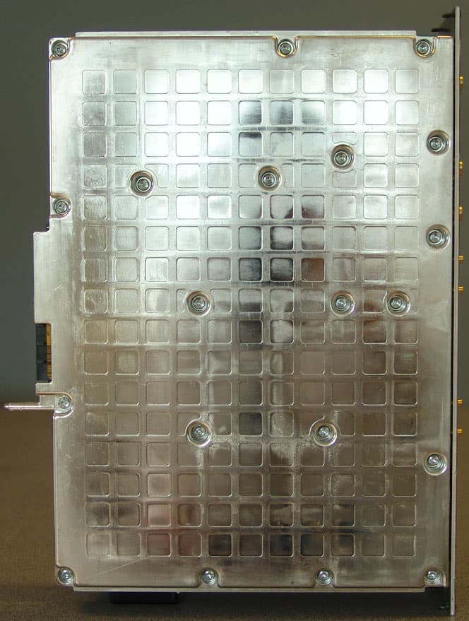
B5KEKRC1311004-2
Jun 13, 2007PCS Broadband GSM Base station transceiver
Equipment Class
PCB - PCS Licensed Transmitter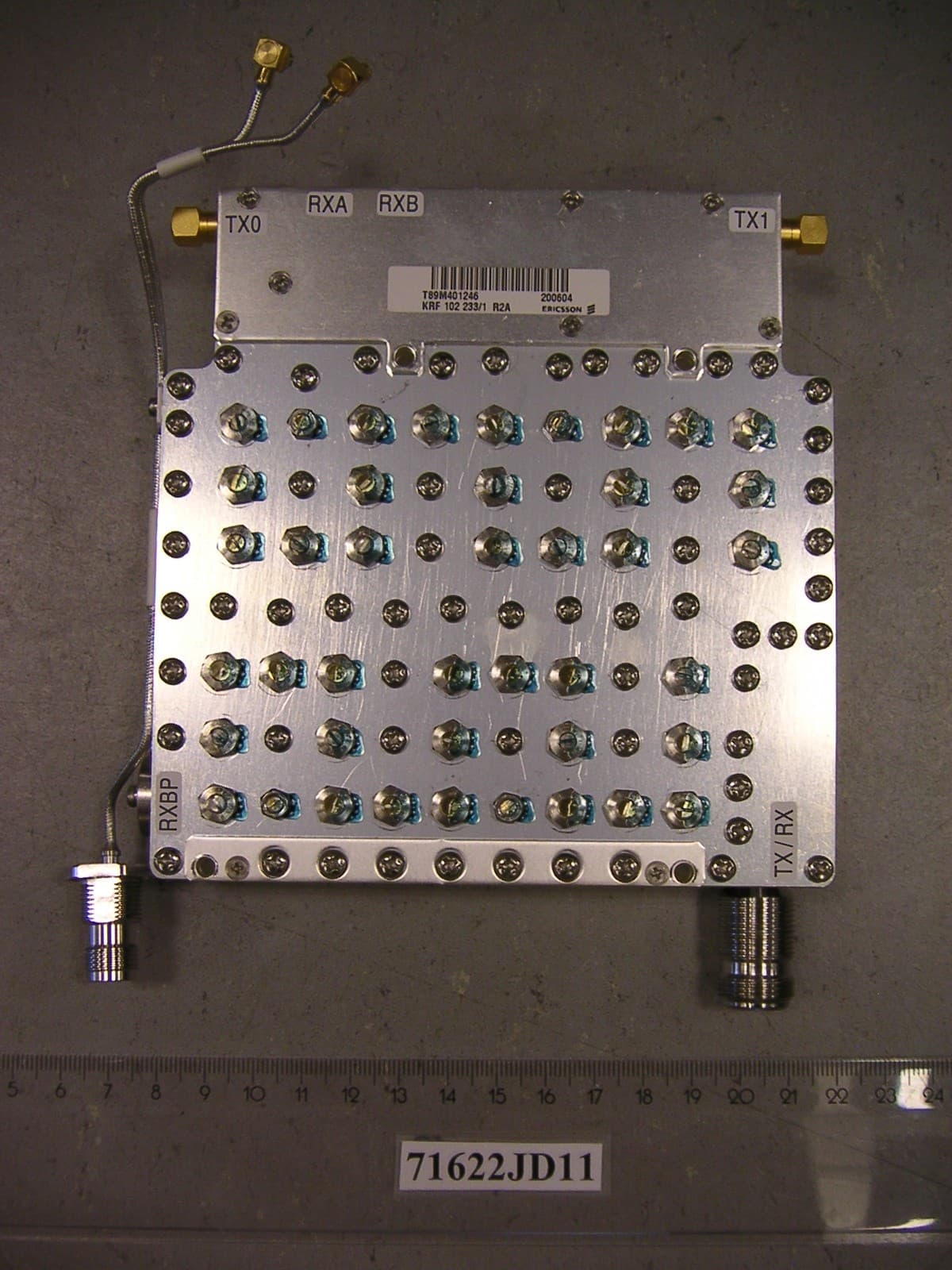
B5KCKRC16184-3
Sep 26, 2006PCS Broadband GSM Base station
Equipment Class
PCB - PCS Licensed Transmitter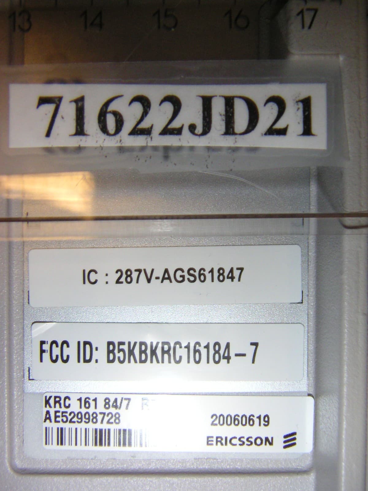
B5KCKRC16184-7
Sep 26, 2006PCS Broadband GSM Base station
Equipment Class
TNB - Licensed Non-Broadcast Station Transmitter
B5KDKRC1311005-2
Sep 06, 2006Broadband GSM Base station transceiver
Equipment Class
TNB - Licensed Non-Broadcast Station Transmitter
B5KAKRC1311013-2
Apr 04, 2005Broadband GSM Base station transceiver
Equipment Class
PCB - PCS Licensed Transmitter