B5KPROJ1192211-1WCDMA Base station
Ericsson Radio Systems AB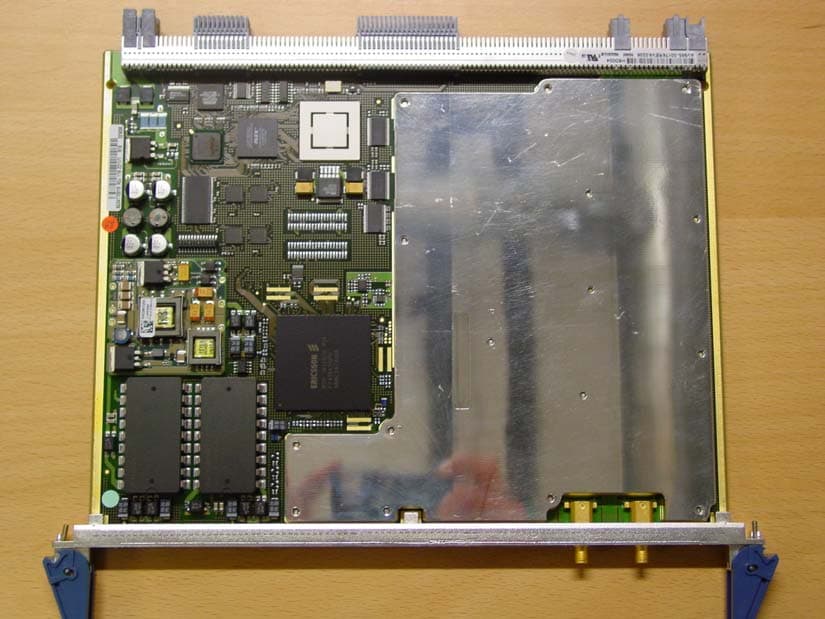
Click to zoom
Application Details
- Equipment Class
- PCB - PCS Licensed Transmitter
- Date of Grant
- Jan 21, 2003
- Application Purpose
- Original Equipment
- Date of Application
- Jan 21, 2003
- Equipment Note
- WCDMA Base station
- Frequency Range
- 1947.50000000 - 1947.50000000
- Company
- Ericsson Radio Systems AB
- Country
- Sweden
Documents & Files
Document Text
Text extracted from the exhibit documents filed with the FCC. Open a document above to read the original.
Users Manual
Open Information DESCRIPTION1 ( 12 ) EIN/R/I Maude Andersson1/1553-COH 109 334/1 Uen ERA/RGG/THC2002-05-31B Prepared (also subject responsible if other)No ApprovedCheckedDateRevReference E Product Data ContentsPage 1Product Data RBS 3202 . . . . . . . . . . . . . . . . . . . . . . . . . . . . . . . . . . . . . . . . . . . . . . . . . . . . . . . . .2 1.1Introduction . . . . . . . . . . . . . . . . . . . . . . . . . . . . . . . . . . . . . . . . . . . . . . . . . . . . . . . . . . . . . . . . . . . . . . . .2 1.2Technical Data . . . . . . . . . . . . . . . . . . . . . . . . . . . . . . . . . . . . . . . . . . . . . . . . . . . . . . . . . . . . . . . . . . . . .2 1.3Standard Configurations . . . . . . . . . . . . . . . . . . . . . . . . . . . . . . . . . . . . . . . . . . . . . . . . . . . . . . . . .5 1.4External Requirements . . . . . . . . . . . . . . . . . . . . . . . . . . . . . . . . . . . . . . . . . . . . . . . . . . . . . . . . . . .5 1.5Connection Interfaces . . . . . . . . . . . . . . . . . . . . . . . . . . . . . . . . . . . . . . . . . . . . . . . . . . . . . . . . . . . .8 A4 XSEIF R2 Open Information DESCRIPTION2 ( 12 ) EIN/R/I Maude Andersson1/1553-COH 109 334/1 Uen ERA/RGG/THC2002-05-31B Prepared (also subject responsible if other)No ApprovedCheckedDateRevReference E 1Product Data RBS 3202 1.1Introduction This document describes the technical data for engineering the Radio Base Station (RBS) 3202. 1.1.1Purpose The purpose of this document is to provide technical data for the RBS 3202. The data is used for installation engineering purposes and no functionality is described in this document. The data is structured as follows: •Physical characteristics such as dimensions, footprints, and weight are described in chapter 1.2. •Standard configurations are described in chapter 1.3. •External requirements such as grounding, climate control, power, and physical site specifications are described in chapter 1.4. •Connection interfaces are described in chapter 1.5. 1.1.2Target Group This document is written for all personnel involved in the implementation activity of the site installation engineering. Personnel working on Ericsson products or systems must have the training and competence required to perform their work correctly. 1.2Technical Data This section provides the following technical data for the RBS 3202: •Overview (chapter 1.2.1) •Dimensions and footprint (chapter 1.2.2) •Weight (chapter 1.2.3 ) 1.2.1Overview The RBS 3202 is a Macro RBS cabinet and can be installed in a building or in a shelter. It is assembled and tested at the factory and delivered equipped according to the standard configuration. Open Information DESCRIPTION3 ( 12 ) EIN/R/I Maude Andersson1/1553-COH 109 334/1 Uen ERA/RGG/THC2002-05-31B Prepared (also subject responsible if other)No ApprovedCheckedDateRevReference E Figure 1RBS 3202 Main Components The RBS 3202 consists of the following main components (see figure 1): •Cabinet top The cabinet top consists of the following components: −Connection Field (CF) position T −Left antenna connection interface position H −Right antenna connection interface position J −Power connection interface position P −Grounding connection interfaces •Capacitor Unit (CU) including fans position D •Baseband (BB) subrack position C and Fan Unit The BB subrack typically consists of the following components: −Baseband Interface Board (BBIFB) −Exchange Terminal Board (ETB) −General Purpose Processor Board (GPB) −Random Access Receiver Board (RAXB) −Switch Core Board (SCB) −Timing Unit Board (TUB) −Transmitter Board (TXB) •Radio Frequency (RF) subrack position B and Fan Unit The RF subrack typically consists of the following components: −Air Interface Unit (AIU) −Radio Frequency Interface Board (RFIFB) −SCB −Transceiver Board (TRXB) •Multicarrier Power Amplifier (MCPA) subrack position A and Fan Unit Open Information DESCRIPTION4 ( 12 ) EIN/R/I Maude Andersson1/1553-COH 109 334/1 Uen ERA/RGG/THC2002-05-31B Prepared (also subject responsible if other)No ApprovedCheckedDateRevReference E The MCPA subrack typically consists of the following components: −MCPA −MCPA Hub 1.2.2Dimensions and Footprint figure 2 shows the RBS 3202 cabinet with dimensions. Figure 2RBS 3202 Cabinet Dimensions, with Base The RBS 3202 cabinet dimensions are the following: Cabinet width 600 mm Cabinet depth without door 400 mm Total cabinet depth including door 450 mm Cabinet height without base 1650 mm Height of base 55 mm Total cabinet height including base 1705 mm Height of locking bar (while in transport mode) 70 mm Height of power connection box 120 mm Adjustable feet, height variation 0mmto10mm figure 3 shows the RBS 3202 footprint with dimensions. Figure 3Base with Dimensions (mm) The overall dimensions for the base are the following: Width 600 mm Depth 400 mm Height 50 mm 1.2.3Weight The weight of the cabinet and base are the following: Open Information DESCRIPTION5 ( 12 ) EIN/R/I Maude Andersson1/1553-COH 109 334/1 Uen ERA/RGG/THC2002-05-31B Prepared (also subject responsible if other)No ApprovedCheckedDateRevReference E RBS 3202 cabinet, fully equipped200 kg Base10 kg 1.3Standard Configurations This section provides information about the standard configurations for the RBS 3202. The following configurations exist: •The 1 x 1 configuration has one sector and one carrier. •The 2 x 1 configuration has two sectors and one carrier. •The 3 × 1 configuration has three sectors and one carrier. This configuration has two transmission solutions: ET-M1 and ET-M4. 1.4External Requirements This section provides information about external site requirements for the RBS 3202. The following requirements are described in this section: •Grounding requirements (chapter 1.4.1) •Power requirements (chapter 1.4.2) •Physical site requirements (chapter 1.4.3) •Climate control requirements (chapter 1.4.4) 1.4.1Grounding Requirements All cabinets are connected to the same grounding point in the equipment room. For more informatio…
Text truncated - open the document above for the full version.
Block Diagram
Open EXHIBIT 4 1 (5) Prepared (also subject responsible if other) No. ERA/RKF/VR Larry Lindström B5KPROJ1192211-1 Approved Checked Date Rev Reference KI/ERA/RKF/VR (L Lindström) 2002-11-08 A 1 EXHIBIT 4 – BLOCK DIAGRAMS Contents 1 EXHIBIT 4 – BLOCK DIAGRAMS 1 1.1 TRXB 1900 MHz WCDMA 1911-ROJ 119 2211/1 2 1.2 MCPA First Stage 1900 WCDMA 1913-ROA 117 8766/1 3 1.3 MCPA Second Stage 1900 WCDMA 1913-ROA 117 8810/1 4 1.4 MCPA Third Stage 1900 WCDMA 1913-ROA 117 8811/1 5 FF Product name Document no Sheet 1 1 2 2 3 3 4 4 5 5 6 6 AA CC D Prepared (also subject responsible if other) References Doc respons/Approved Date Rev BB D EE WICTORIA-TRX EED/N/WRC EEDRAU PS1 board TOP C EED/N/WR EEDTWA 2002-09-06 1911-ROJ 119 2211/1 Ux1(35) Prepared (also subject responsible if other) Checked Approved Date Rev No AMT/T/RE Steve Ip AMT/T/L (Steve Schwerdfeger) 2002-07-16 A 1913-ROA 117 8766/1 Uen Security Class Document name Sheet Limited Internal BLOCK DIAGRAM 1 (1) EPA Block Diagram Gain/Loss (dB) Power ( dBm ) 35.5 22 8 -4 -1.5min 13.5 14 -5.5 13.5 4.5 A R1 VVA AT3 Hybrid HY1 A R2 A R3 Hybrid HY2 V401 Hybrid HY3 V402V403 Hybrid HY4 THERMALPAD (3dB) THERMAL PAD (6dB) Prepared (also subject responsible if other) Checked Approved Date Rev No AMT/T/RE (Aleksey Lyalin) AMT/T/L (Steve Schwerdtfeger) 2002-07-11 A 1913-ROA 117 8810/1 Uen Security Class Document name Sheet Limited Internal BLOCK DIAGRAM 1 (1) EPA Block Diagram A R1: AH1 Gain=12.5dB-6dB pad-3dB pad VVA A T3 Set to ñ3.9 dB Hybrid -0.4dB A R2 : SXT 289 Gain=14.5dBA R3 : SXT 289 Gain=14.5dB Hybrid -0.4dB V404 : MRF19030 Gain=13dB Hybrid -0.4dB V405 : MRF19045 Gain=14.5dBV406 : MRF19045 Gain=14.5dB Hybrid -0.4dB -3.5dBm 0 dBm -3.9dBm 9.8 dBm 22.8dBm 36.5 dBm Prepared (also subject responsible if other) Checked Approved Date Rev No AMT/T/RE Frank D'Angelo AMT/T/L (Mike Hrybenko) 7/30/02 A 1913-ROA 117 8811/1 Uen Security Class Document name Sheet Limited Internal BLOCK DIAGRAM 1 (1) MPA Block Diagram V103 V104 V105 T102 -0.3 dB 3-WAY COMB T101 -0.3 dB 3-WAY DIV RF IN RF OUT N102 +5 V REG N101 TEMP SENSE +35.0 dBm +47.5 dBm +43.0 dBm +29.9 dBm P gain total = 12.5 dB Pg = 13.1 dB
Cover Letter(s)
Open EXHIBIT 13 1 (1) Prepared (also subject responsible if other) No. ERA/RKF/VR Larry Lindström Approved Checked Date Rev Reference KI/ERA/RKF/VR (L Lindström) 2002-11-26 A B5KPROJ1192211-1 Federal Communications Commission Authorization & Evaluation Division 7435 Oakland Mills Road Columbia, Maryland 21046 Attention: Equipment Authorization Branch SP Sveriges Provnings- och ForskningsInstitut Brinellgatan 4 Box 857 S-501 15 Borås Sweden November 26, 2002 Subject: Certification for FCC ID: B5KPROJ1192211-1 Gentlemen; Ericsson AB requests a Grant of Certification (Type Acceptance) for the above mentioned FCC Identifier. This base station transceiver and multi carrier power amplifier are designed for use in the WCDMA 1900 MHz cellular telephone system. The transmitter will operate at 1947.5 MHz. The receiver circuit supports 1867.5 MHz. The base station operates in the D-band in the 1900 MHz broadband PCS services as per 47 CFR Part 24 subpart E. It meets the requirements of 3GPP specification for operation in WCDMA cellular systems. This base station will in normal mode operate at a nominal power out of 20 watts at the antenna connector. Ericsson AB requests confidentiality under CFR 0.459. Confidentiality for the following exhibits is requested: Exhibit 5 TRXB Part Exhibit 5 MCPA Part Exhibit 8 Internal Manual Justification of this request is in order to protect the large investment in developing this technology and to facilitate the circuit miniaturization utilized in this design and protect the innovative design as well as proprietary techniques which are implemented. In order to protect Ericsson’s competitive advantage on these proprietary techniques, we request the above listed exhibits be held as confidential and withheld from the Public Information File. If additional information is needed, please contact me on the below listed number. Sincerely, Larry Lindström Staff Engineer, Regulatory Programs Ericsson AB Torshamnsgatan 21-23 (Färögatan 6) Kista, SE-164 80 Stockholm Sweden Telephone No.: +46 8 764 12 73 Fax No.: +46 8 404 44 20 e-mail [email protected]
Cover Letter(s)
Open EXHIBIT 13 1 (1) Prepared (also subject responsible if other) No. ERA/RWG/RB Larry Lindström Approved Checked Date Rev Reference KI/ERA/RWG/RB (L Lindström) 2003-01-15 A B5KPROJ1192211-1 Federal Communications Commission Authorization & Evaluation Division 7435 Oakland Mills Road Columbia, Maryland 21046 Attention: Equipment Authorization Branch SP Sveriges Provnings- och ForskningsInstitut Brinellgatan 4 Box 857 S-501 15 Borås Sweden January 15, 2003 Subject: Complementary Information for Certification for FCC ID: B5KPROJ1192211-1 Gentlemen; Ericsson AB requested a Grant of Certification (Type Acceptance) for the above mentioned FCC Identifier. Here are the complementary information to Your question No 3: 3) Frequency stability data from -30 to -5 degrees centigrade per 2.1055 (a) 1. This base station transceiver and multi carrier power amplifier are designed together with the cabinet and other boards for use in a temperature range of +5º C to +40º C. The base station transceiver (TRXB) is equipped with a thermal sensor that shut down the exciter power amplifier in the TRXB in a controlled way at temperatures below +3º C and above + 52º C. The frequency stabilizing circuitry and the MCPA are still in stand-by mode below and above these temperatures to be prepared to transmit with proper function if the environment temperature reaches the applicable temperature range again. There is also a non- destruction tempereture range outside the range above where the base station is shut down totally. If additional information is needed, please contact me on the below listed number. Sincerely, Larry Lindström Staff Engineer, Regulatory Programs Ericsson AB Torshamnsgatan 21-23 (Färögatan 6) Kista, SE-164 80 Stockholm Sweden Telephone No.: +46 8 764 12 73 Fax No.: +46 8 404 44 20 e-mail [email protected]
Cover Letter(s)
1) Letter requesting confidentiality of appropriate exhibits. Unfortunately the cover letter was by mistake not uploaded 11/27/2002. Will be uploaded with the new filing. 2) Block diagrams. There was no request from the filing system about this and therefore not uploaded. It will be uploaded with the new filing 3) Frequency stability data from -30 to -5 degrees centigrade per 2.1055 (a) 1 and for voltage variation to +15%. The unit’s normal operation conditions (specified in the manual, enclosed in this letter) are +5 to +40 deg Celsius. According to the manufacturer the unit will shut down if going below + 5 deg Celsius. I have talked to the test lab engineer and he confirmed that the unit does not worked at 0 deg Celsius. A cover letter with complementary information from the manufacturer will be uploaded in the new filing. About the frequency stability vs. voltage variation ±15% In the report (enclosure 7) it is stated that the measurement were done at 54.2V. I have talked to the test lab engineer and he told me that it has been a type error in the report. The measurement was done at -40.8 V and at 55.2V. A revised report is produced which corrects this and will be uploaded with the new filing. 4) Comprehensive details of the procedures, equipment and equipment settings for the spurious radiation emission tests. The information is included in the revised report 5) Data demonstrating compliance with block edge requirements of 24.238. Please use 1 MHZ RBW as specified. Equipment must comply at 1 MHz from block edge or a waiver of the requirement authorized. An additional report will be uploaded with the new filing with measurements done with a sharper 1MHz filter to fulfil the current rules. The filter used is incorporated in the new Spectrum analyser, FSU from Rohde & Schwarz and is called “channel filter”. It has a shape factor of <2. The report also shows measurements according to the new rules (February 18). 6) Please update the frequency range on Form 731. The range should contain a single frequency. Will be updated with the new filing 7) Clarification of the nature of the granted equipment. Is the grant for a complete base station or for the two modules specifically mentioned? Can the base station contain other/different transmitter modules not mentioned in this filing? The grant is for the two modules specifically mentioned. The base station does not contain any other transmitter modules. 1 Tomas Bodeklint Från: Jan Welinder Skickat: den 30 december 2002 08:08 Till: Tomas Bodeklint Ämne: VB: Request for additional information -----Ursprungligt meddelande----- Från: [email protected] [mailto:[email protected]] Skickat: den 20 december 2002 18:56 Till: Jan Welinder Ämne: Request for additional information To: Jan Welinder From: Martin Perrine [email protected] FCC Equipment Authorization Branch Re: FCC ID: B5KPROJ1192211-1 Applicant: Ericsson Radio Systems AB Correspondence Reference Number: 6259 731 Confirmation Number: TC971248 Date of Original Email: 12/20/2002 Subject: Request for additional information In regards to your recent TCB grant referenced above we kindly request that you provide the following additional information. To avoid consequences to grant please provide data for question 5 by COB 26 December. Call Martin Perrine at 301 362 3025 to discuss if desired. 1) Letter requesting confidentiality of appropriate exhibits. 2) Block diagrams. 3) Frequency stability data from -30 to -5 degrees centigrade per 2.1055 (a) 1 and for voltage variation to +15%. 4) Comprehensive details of the procedures, equipment and equipment settings for the spurious radiation emission tests. 5) Data demonstrating compliance with block edge requirements of 24.238. Please use 1 MHZ RBW as specified. Equipment must comply at 1 MHz from block edge or a waiver of the requirement authorized. 6) Please update the frequency range on Form 731. The range should contain a single frequency. 7) Clarification of the nature of the granted equipment. Is the grant for a complete base station or for the two modules specifically mentioned? Can the base station contain other/different transmitter modules not mentioned in this filing? The items indicated above must be submitted before processing can continue on the above referenced application. Failure to provide the requested information within 30 days of the original e-mail date may result in application dismissal pursuant to Section 2.917(c). DO NOT Reply to this email by using the Reply button. In order for your response to be processed expeditiously, you must upload your response via the Internet at www.fcc.gov, E-Filing, OET TCB Electronic Filing, TCB Login. If the response is 2 submitted through Add Attachments, a message which informs the processing staff that a new exhibit has been submitted must also be submitted via Submit Correspondence. Also, please note that partial responses increase processing time and should not be submitted. Any questions about the content of this correspondence should be directed to the e- mail address listed below the name of the sender.
External Photos
REPORT Datum/Date Beteckning/Reference Sida/Page 2002-10-25 F219009-F24 1 (5) FCC ID: B5KPROJ1192211-1 Encl. 9 Transceiver Unit, ROJ 119 2211/1, R1B Front side Top REPORT Datum/Date Beteckning/Reference Sida/Page 2002-10-25 F219009-F24 2 (5) FCC ID: B5KPROJ1192211-1 Encl. 9 Bottom side ID Label FCC ID: REPORT Datum/Date Beteckning/Reference Sida/Page 2002-10-25 F219009-F24 3 (5) FCC ID: B5KPROJ1192211-1 Encl. 9 Amplifier Unit / MCPA, KRB 90102/3, R1A Front side Top REPORT Datum/Date Beteckning/Reference Sida/Page 2002-10-25 F219009-F24 4 (5) FCC ID: B5KPROJ1192211-1 Encl. 9 Bottom side ID label REPORT Datum/Date Beteckning/Reference Sida/Page 2002-10-25 F219009-F24 5 (5) FCC ID: B5KPROJ1192211-1 Encl. 9 FCC ID
ID Label/Location Info
REPORT Datum/Date Beteckning/Reference Sida/Page 2002-10-25 F219009-F24 1 (2) FCC ID: B5KPROJ1192211-1 Encl. 9 Transceiver Unit, ROJ 119 2211/1, R1B FCC ID Label Label placement REPORT Datum/Date Beteckning/Reference Sida/Page 2002-10-25 F219009-F24 2 (2) FCC ID: B5KPROJ1192211-1 Encl. 9 Amplifier Unit / MCPA, KRB 90102/3, R1A FCC ID Label Label placement
Internal Photos
REPORT Datum/Date Beteckning/Reference Sida/Page 2002-10-25 F219009-F24 1 (7) FCC ID: B5KPROJ1192211-1 Encl. 9 Transceiver Unit, ROJ 119 2211/1, R1B Main board- PCB component side Main board- PCB rear side REPORT Datum/Date Beteckning/Reference Sida/Page 2002-10-25 F219009-F24 2 (7) FCC ID: B5KPROJ1192211-1 Encl. 9 Amplifier Unit / MCPA, KRB 90102/3, R1A Printed Board MCPA Radio Control ROA 128 0185/1 with lid REPORT Datum/Date Beteckning/Reference Sida/Page 2002-10-25 F219009-F24 3 (7) FCC ID: B5KPROJ1192211-1 Encl. 9 Printed Board MCPA Radio Control ROA 128 0185/1 Backside Printed Board MCPA Radio Control ROA 128 0185/1 REPORT Datum/Date Beteckning/Reference Sida/Page 2002-10-25 F219009-F24 4 (7) FCC ID: B5KPROJ1192211-1 Encl. 9 Backside lid for Printed Board MCPA Radio Control ROA 128 0185/1 Printed Board MCPA Control Stage 1 ROA 117 8633/1 REPORT Datum/Date Beteckning/Reference Sida/Page 2002-10-25 F219009-F24 5 (7) FCC ID: B5KPROJ1192211-1 Encl. 9 Printed Board MCPA Control Stage 1 ROA 117 8497/1 Power Ampliflier Block KRY 901 001/1 with lid REPORT Datum/Date Beteckning/Reference Sida/Page 2002-10-25 F219009-F24 6 (7) FCC ID: B5KPROJ1192211-1 Encl. 9 Power Ampliflier Block KRY 901 001/1 with Printed Board MCPA Second Stage ROA 117 8810/1 Power Ampliflier Block KRY 901 001/1 with Printed Board MCPA Third Stage ROA 117 8811/1 REPORT Datum/Date Beteckning/Reference Sida/Page 2002-10-25 F219009-F24 7 (7) FCC ID: B5KPROJ1192211-1 Encl. 9 Power Ampliflier Block KRY 901 001/1 with Printed Board MCPA First Stage ROA 117 8766/1
Operational Description
Open EXHIBIT 12 1 (13) Prepared (also subject responsible if other) No. ERA/RKF/VR Larry Lindström B5KPROJ1192211-1 Approved Checked Date Rev Reference KI/ERA/RKF/VR (L Lindström) 2002-11-20 A Exhibit 12 – Cover Sheet Contents 1 2.1033(c) Circuit Description 2 1.1 (2) FCC Identifier: B5KPROJ1192211-1 2 1.2 (4) Type of Emission: 4M20F9W 2 1.3 (5) Frequency range: 1945 to 1950 MHz 2 1.4 (6) Range of Operating Power: 2 1.5 (7) Maximum Power Rating: 2 1.6 (8) Final Amplifier Voltage and Current in normal operation 2 1.7 (10) Frequency Stabilizing Circuit Description 3 1.8 (10) Spurious and Harmonic Suppression 3 1.9 (10) Limiting Power 3 1.10 (10) Digital Modulation QPSK 4 Open EXHIBIT 12 2 (13) Prepared (also subject responsible if other) No. ERA/RKF/VR Larry Lindström B5KPROJ1192211-1 Approved Checked Date Rev Reference KI/ERA/RKF/VR (L Lindström) 2002-11-20 A 1 2.1033(c) Circuit Description 1.1 (2) FCC Identifier: B5KPROJ1192211-1 This TRXB (Tranceiver Radio Unit) and MCPA (Multi Carrier Power Amplifier) consist of one synthesized transmitter operating in the frequency band of 1945 to 1950 MHz. There are ONE Channel available. The transmitter is capable of operation in a WCDMA system. For each channel there are 64 code slots available,each containing digital speech or data for QPSK. 1.2 (4) Type of Emission: 4M20F9W 1.3 (5) Frequency range: 1945 to 1950 MHz 1.4 (6) Range of Operating Power: This transmitter is designed to supply a nominal power level of 43 dBm at the antenna connector. 1.5 (7) Maximum Power Rating: The maximum power rating with one TRX under environmental and supply voltage variations is equal to 43 dBm plus a power level tolerance of + 1.0 dB. Therefore the maximum output power is 44 dBm equal to 25 W at the antenna connector of the radio base station. 1.6 (8) Final Amplifier Voltage and Current in normal operation Average Output Power 43 dBm Values for V103, V104 and V105 Collector Voltage 28.0 Volt DC Collector Current 10.5 Amps DC Open EXHIBIT 12 3 (13) Prepared (also subject responsible if other) No. ERA/RKF/VR Larry Lindström B5KPROJ1192211-1 Approved Checked Date Rev Reference KI/ERA/RKF/VR (L Lindström) 2002-11-20 A 1.7 (10) Frequency Stabilizing Circuit Description The TRXB frequency chain is as follows: The TRXB have two stabilizing clock circuits, one 10 MHz VCXO and one 61.44 MHz VCXO. Both these clocks are phase-locked to a incoming 30.72 MHz clock reference. The 61.44 MHz clock is fed to the Digital to Analog Converter in the transmit chain and to the Analog to Digital Converter in the receive chain. The base band signal fed to the Digital to Analog Converter is digitally QPSK IQ-modulated. The output from the Digital to Analog Converter have a frequency of 15.36 MHz. This signal is mixed with a 272.64 MHz signal from the Transmit Intermediate Local Oscillator (PLL) to 288 MHz. The Transmit Intermediate Local Oscillator is phase-locked to the 10 MHz signal from the VCXO above. The 288 MHz signal is then mixed with a signal of 1644.5 to 1699.5 MHz from one of two Local Oscillators to 1932.5 to 1987.5 MHz. The Local Oscillators are phase-locked to the same 10 MHz signal from the VCXO above. (In this case is the output frequency locked to 1947.5 MHz – LO frequency of 1659.5 MHz). The 30.72 MHz clock reference is generated in a voltage controlled oscillator placed in the Timing Unit Board (TUB). This clock is phase-locked to a 8 kHz oscillator also placed in the TUB. This oscillator is in turn locked to the extracted frame-sync of 8 kHz from the Exchange TerMinal board (ETM). The ETM is connected to the incoming PCM-link, where the frame-sync from the PCM is extracted. As an option can the TUB be directly connected to external PCM-links or a 10 MHz source. 1.8 (10) Spurious and Harmonic Suppression Spurious and harmonic suppression is achieved by using two separate bandpass filters of ceramic type in the exciter (in TRXB). A filter module at the output (in TRXB) works like a bandpass filter around the carrier. In addition to these filters, the output signal (from MCPA) passes a cavity band pass filter in the antenna interface system (AIU). 1.9 (10) Limiting Power The TRXB measures the output power at its output connector via a RF-detector and the detected value is used by the power loop control block to steer the variable gain amplifiers beteween the modulator and the exciter amplifier. The MCPA measures the output power at its output connector via a RF-detector and the detected value is used by the power loop control block to steer the three amplifiers between the input and the output of the amplifier. Open EXHIBIT 12 4 (13) Prepared (also subject responsible if other) No. ERA/RKF/VR Larry Lindström B5KPROJ1192211-1 Approved Checked Date Rev Reference KI/ERA/RKF/VR (L Lindström) 2002-11-20 A 1.10 (10) Digital Modulation QPSK 5 Downlink spreading and modulation 5.1 Spreading Figure 8 illustrates the spreading operation for all downlink physical channels except SCH, i.e. for P-CCPCH, S-CCPCH, CPICH, AICH, AP-AICH, CD/CA-ICH, PICH, CSICH, PDSCH, and downlink DPCH. The non-spread physical channels except SCH, AICH, AP-AICH and CD/CA-ICH consist of a sequence of 3-valued digits taking the values 0, 1, "DTX". Note that "DTX" is only applicable to those downlink physical channels that support DTX transmission. Before the spreading operation, these are mapped to real-valued symbols as follows: the binary value "0" is mapped to the real value +1, the binary value "1" is mapped to the real value –1 and "DTX" is mapped to the real value 0. For the indicator channels using signatures (AICH, AP-AICH and CD/CA-ICH), the real-valued symbols depend on the exact combination of the indicators to be transmitted, compare [2] sections 5.3.3.7, 5.3.3.8 and 5.3.3.9. Each pair of two consecutive real-valued symbols is first serial-to-parallel converted and mapped to an I and Q branch. The mapping is such that even and odd numbered symbols are mapped to the I and Q branch respectively.…
Text truncated - open the document above for the full version.
Parts List/Tune Up Info
Open EXHIBIT 10 1 (17) Prepared (also subject responsible if other) No. ERA/RKF/VR Larry Lindström B5KPROJ1192211-1 Approved Checked Date Rev Reference KI/ERA/RKF/VR (L Lindström) 2002-11-20 A Exhibit 10 – Components, Tune Up Contents 1 2.1033 (c) (10) Function of Active Circuit Devices..........................2 1.1 Transceiver TRXB WCDMA ROJ 119 2211/1.................................2 1.1.1 Printed Board ROJ 119 2211/1........................................................2 1.2 Multi Carrier Power Amplifier MCPA WCDMA KRB 901 02/3........6 1.2.1 Power Amplifier Block KRY 901 001/1............................................6 1.2.1.1 Printed Board MCPA First Stage 1900 WCDMA ROA 117 8766/16 1.2.1.2 Printed Board MCPA Second Stage 1900 WCDMA ROA 117 8810/1 7 1.2.1.3 Printed Board MCPA Third Stage 1900 WCDMA ROA 117 8811/18 1.2.1.4 Power Amplifier Block KRY 901 001/1............................................9 1.2.2 MCPA Control Unit Block KRY 112 64/3......................................10 1.2.2.1 MCPA Control Stage 1 1900 WCDMA ROA 117 8497/1..............10 1.2.2.2 MCPA Control Stage 2 1900 WCDMA ROA 117 8633/1..............11 1.2.2.3 Printed B. MCPA Radio Control 1900 WCDMA ROA 128 0185/112 2 2.1033(c)(9) Tune-Up Procedure...................................................16 3 2.1033(c)(9,10) Power Tune-Up – Power Limiting........................17 Open EXHIBIT 10 2 (17) Prepared (also subject responsible if other) No. ERA/RKF/VR Larry Lindström B5KPROJ1192211-1 Approved Checked Date Rev Reference KI/ERA/RKF/VR (L Lindström) 2002-11-20 A 1 2.1033 (c) (10) Function of Active Circuit Devices 1.1 Transceiver TRXB WCDMA ROJ 119 2211/1 1.1.1 Printed Board ROJ 119 2211/1 Product ROJ 119 2211/1 Revision D Pos Prod name/Des Product number D1 MICROCIRCUIT/74'16244 LVTH TSSOP48 16x BUFF RYT 329 6001/C D4 MICROCIRCUIT/10K100E-2 3.3V C=0/70 RYT 141 6011/C D5 MICROCIRCUIT/FLASH TB 2M16 90NS 3.3V I RYT 118 6152/6 D6 MICROCIRCUIT/FLASH TB 2M16 90NS 3.3V I RYT 118 6152/6 D8 MICROCIRCUIT/PPC403GCX-80 RYT 123 6046/4C D10 ASIC/SPIC-MZ ROP 101 1149/2 D12 MICROCIRCUIT/DRAM EDO 4M16 50NS 3.3V C RYT 119 6056/1 D13 MICROCIRCUIT/DRAM EDO 4M16 50NS 3.3V C RYT 119 6056/1 D14 MICROCIRCUIT/7128AE-7 3.3V C=0/70 RYT 141 6006/4C D15 MICROCIRCUIT/74'14 Z1G SOT23-5 1X SCHMITT I RYT 326 6014/41C D16 OSCILLATOR/19.44 MHz RTL 201 629/24 D20 MICROCIRCUIT/FLASH TB 2M16 90NS 3.3V I RYT 118 6152/6 D21 MICROCIRCUIT/FLASH TB 2M16 90NS 3.3V I RYT 118 6152/6 D96 MICROCIRCUIT/DRAM EDO 4M16 50NS 3.3V C RYT 119 6056/1 D97 MICROCIRCUIT/DRAM EDO 4M16 50NS 3.3V C RYT 119 6056/1 D98 MICROCIRCUIT/74'02 Z1G SSOP5-P-A 1x 2-INP N RYT 326 6002/42C D1001 PRODUKTANPASS. KRETS/ASIC SURVEYOR_2, TRX-DIG ROP 101 25/2 D1002 MICROCIRCUIT/74'16374 LVTH TSSOP48 16x D-TY RYT 329 6004/C D1003 MICROCIRCUIT/74'16374 LVTH TSSOP48 16x D-TY RYT 329 6004/C D1004 MICROCIRCUIT/74'16244 LVTH TSSOP48 16x BUFF RYT 329 6001/C D1005 MICROCIRCUIT/ECL TRANSLATOR LVPECL:LVTTL x2 RYT 407 6008/C D1006 MICROCIRCUIT/74'74 LVT TSSOP14 2xD FLIP-FLO RYT 329 0074/C D2080 MICROCIRCUIT/74'04 Z1G SSOP5-P-A 1x INVERTE RYT 326 6004/42C D2180 MICROCIRCUIT/74'04 Z1G SSOP5-P-A 1x INVERTE RYT 326 6004/42C D2600 MICROCIRCUIT/10-bit serial AD conv. 0.5LSB RYT 120 6070/1 D2602 FILTER/1960MHz BP RTN 202 814/02 D2603 MICROCIRCUIT/OPAMP x2 3.6-16V 1.40MHz RYT 101 6043/2C D2604 FILTER/1946.5MHz BP RTN 202 1007/02 D2605 FILTER/1973.5MHz BP RTN 202 1008/02 D2700 MICROCIRCUIT/10-bit serial AD conv. 0.5LSB RYT 120 6070/1 D2702 FILTER/1960MHz BP RTN 202 814/02 D2704 FILTER/1946.5MHz BP RTN 202 1007/02 Open EXHIBIT 10 3 (17) Prepared (also subject responsible if other) No. ERA/RKF/VR Larry Lindström B5KPROJ1192211-1 Approved Checked Date Rev Reference KI/ERA/RKF/VR (L Lindström) 2002-11-20 A D2705 FILTER/1973.5MHz BP RTN 202 1008/02 D2706 MICROCIRCUIT/OPAMP x2 3.6-16V 1.40MHz RYT 101 6043/2C D3000 MICROCIRCUIT/Amplifier. GaAs MMIC RYT 101 6479/2 D3001 FILTER/1880MHz BP RTN 202 1006/02 D3002 MIXER/SYM-20DHW RYT 901 6170/1 D3010 MICROCIRCUIT/Amplifier. GaAs MMIC RYT 101 6479/2 D3011 FILTER/1880MHz BP RTN 202 1006/02 D3012 MIXER/SYM-20DHW RYT 901 6170/1 D3301 FILTER/208MHz BP SAW RTN 201 402/01 …
Text truncated - open the document above for the full version.
Contact Information
Applicant
Bo Bergstrom(Manager)
+468 757 0401Fax: +468 751 4687
Technical Contact
Ericsson Radio Systems ABLarry Lindstrom
[email protected]+46 8 764 1273
Torshamnsgatan 21-23 · SE-164 80 Stockholm · Sweden
Test Firm
SP Technical Research Institute of SwedenMagnus Winehem
Technical Specifications
| # | Rule Parts | Frequency Range | Power Output | Emission | Tolerance |
|---|---|---|---|---|---|
| 1 | 24E | 1.95 GHz - 1.95 GHz | 20 W | 4M20F9W | 0.0500000000 ppm |
Other Applications from Ericsson Radio Systems AB
B5KEKRC1311004-2
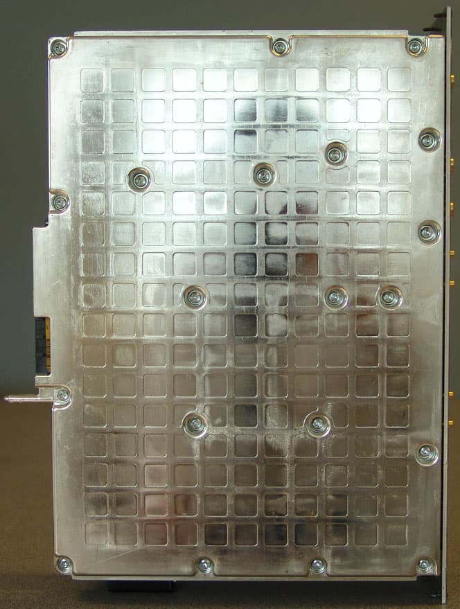
Jun 13, 2007PCS Broadband GSM Base station transceiver
Equipment Class
PCB - PCS Licensed Transmitter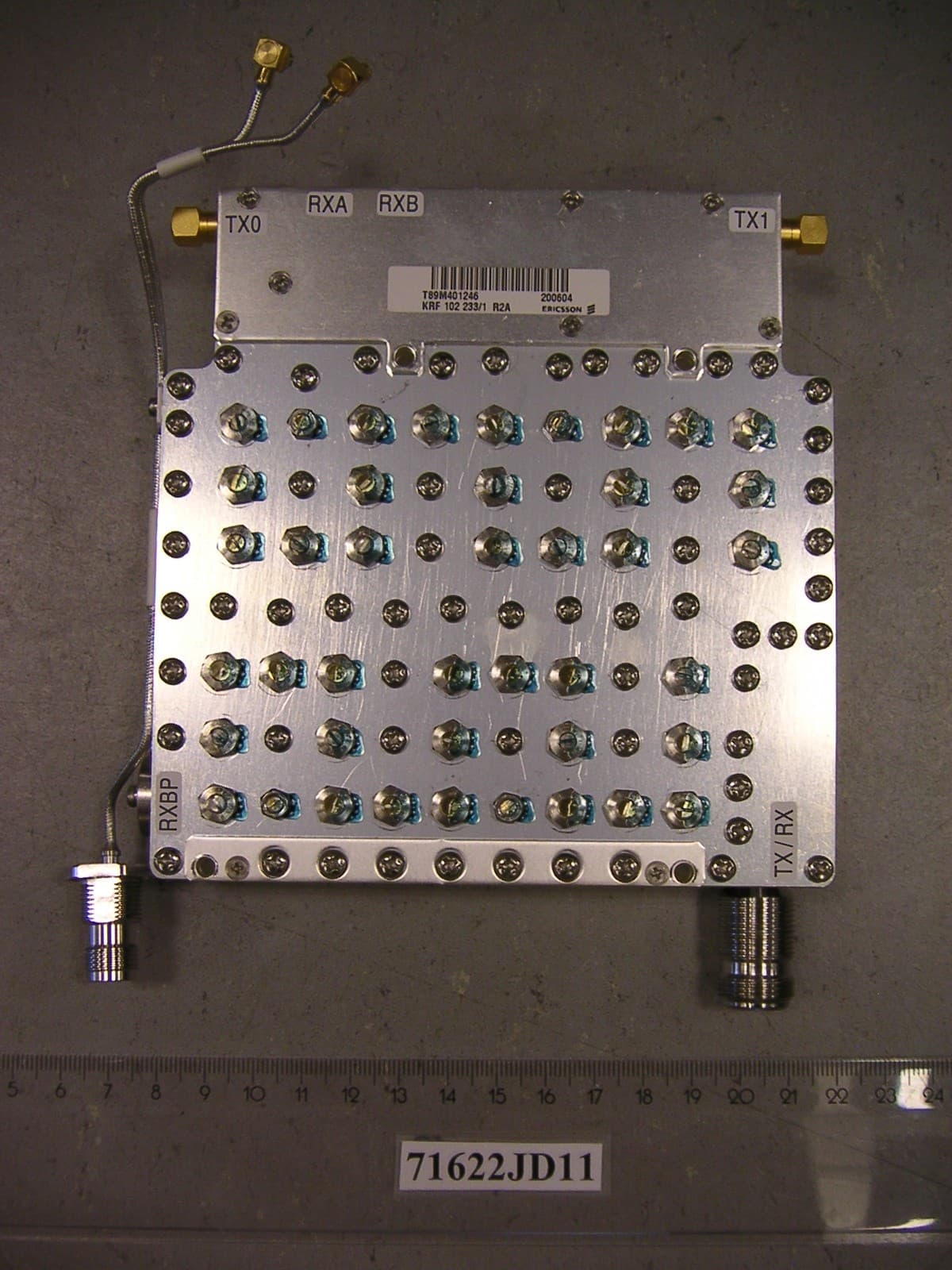
B5KCKRC16184-3
Sep 26, 2006PCS Broadband GSM Base station
Equipment Class
PCB - PCS Licensed Transmitter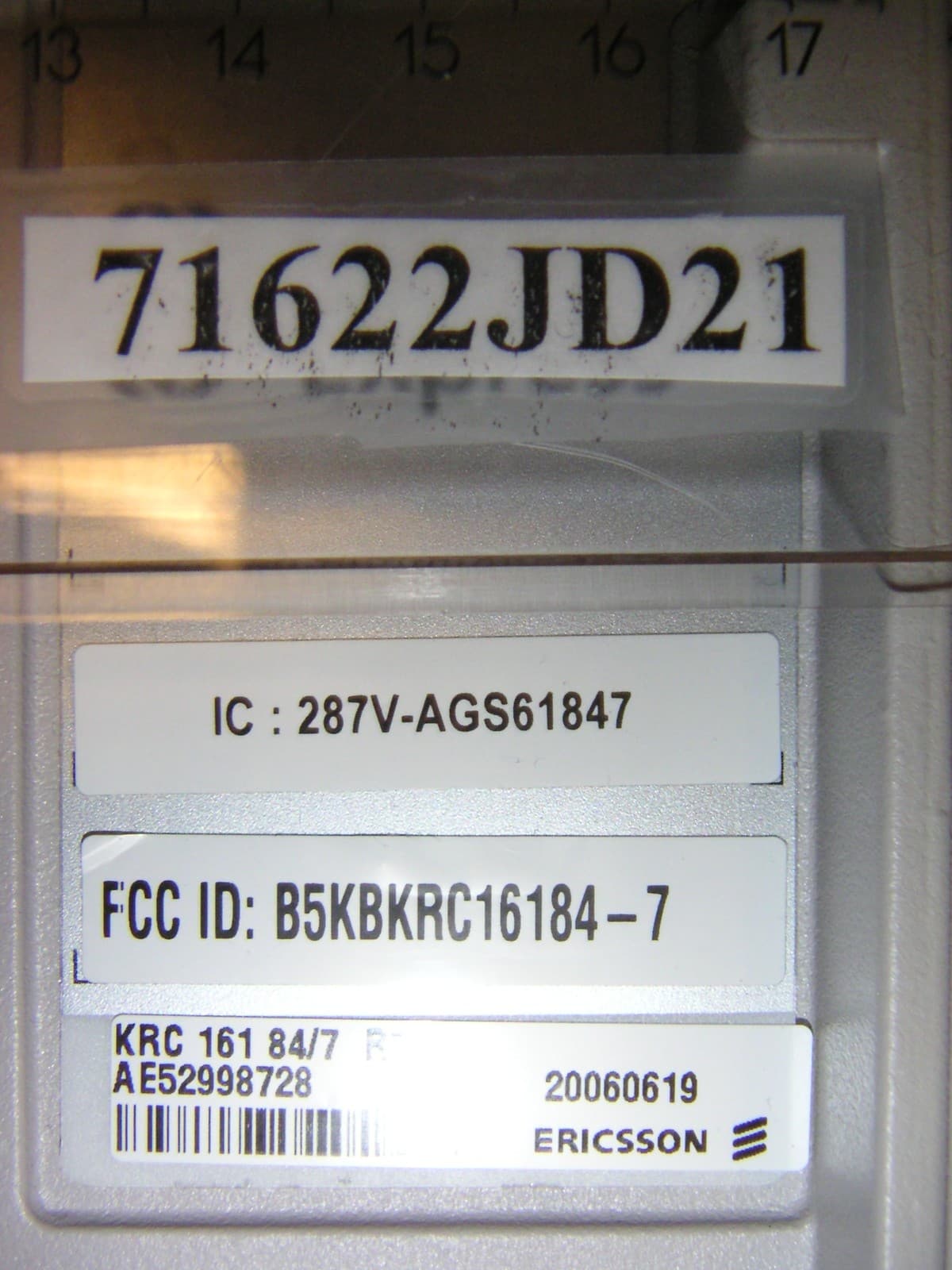
B5KCKRC16184-7
Sep 26, 2006PCS Broadband GSM Base station
Equipment Class
TNB - Licensed Non-Broadcast Station Transmitter
B5KDKRC1311005-2
Sep 06, 2006Broadband GSM Base station transceiver
Equipment Class
TNB - Licensed Non-Broadcast Station Transmitter
B5KAKRC1311013-2
Apr 04, 2005Broadband GSM Base station transceiver
Equipment Class
PCB - PCS Licensed Transmitter