BBD3-KVC8ARF Power Amplifier
TPL Communications Inc
Click to zoom
Application Details
- Equipment Class
- TNB - Licensed Non-Broadcast Station Transmitter
- Date of Grant
- May 24, 2001
- Application Purpose
- Original Equipment
- Date of Application
- Feb 14, 2001
- Equipment Note
- RF Power Amplifier
- Frequency Range
- 150.00000000 - 174.00000000
- Company
- TPL Communications Inc
- Country
- United States
Documents & Files
Document Text
Text extracted from the exhibit documents filed with the FCC. Open a document above to read the original.
Users Manual
Appendix AFCC ID: BBD6-KVC8A A1 Appendix AFCC ID: BBD6-KVC8A A2 Appendix AFCC ID: BBD6-KVC8A A3 Appendix AFCC ID: BBD6-KVC8A A4 Appendix AFCC ID: BBD6-KVC8A A5 Appendix AFCC ID: BBD6-KVC8A A6 Appendix AFCC ID: BBD6-KVC8A A7 Appendix AFCC ID: BBD6-KVC8A A8 Appendix AFCC ID: BBD6-KVC8A A9 Appendix AFCC ID: BBD6-KVC8A A10 Appendix AFCC ID: BBD6-KVC8A A11 Appendix AFCC ID: BBD6-KVC8A A12 Appendix AFCC ID: BBD6-KVC8A A13
Users Manual
Appendix AFCC ID: BBD6-KVC8A A1 Appendix AFCC ID: BBD6-KVC8A A2 Appendix AFCC ID: BBD6-KVC8A A3 Appendix AFCC ID: BBD6-KVC8A A4 Appendix AFCC ID: BBD6-KVC8A A5 MAXIMUM PERMISSIBLE EXPOSURE In order to meet the FCC’s Maximum Permissible Exposure (MPE) limit for General Population/Uncontrolled Exposure of 27.5 V/m, the end user must install the antenna used with this amplifier on the vehicle such that the unobstructed line of sight distance from the antenna to any person is at least the MPE distance of 25.7 cm. Appendix AFCC ID: BBD6-KVC8A A6 Appendix AFCC ID: BBD6-KVC8A A7 Appendix AFCC ID: BBD6-KVC8A A8 Appendix AFCC ID: BBD6-KVC8A A9 Appendix AFCC ID: BBD6-KVC8A A10 Appendix AFCC ID: BBD6-KVC8A A11 Appendix AFCC ID: BBD6-KVC8A A12
Cover Letter(s)
Hi, We are submitting a new exhibit that was requested by Correspondence Reference Number 18865 for Confirmation Number EA100059. The two new exhibits are: A updated Users Manual and New Test Report. If you have any questions please feel free to contact Bryan Broaddus ([email protected]) at any time. Thank You, Bryan Broaddus
External Photos
FCC ID: BB Photo 3External Front View FCC ID: BB Photo 4External ¾ View
ID Label/Location Info
FCC ID: BB 2.1033 (C) (11)Equipment Identification Plate _______________________________________ KENWOOD VEHICULAR ADAPTER MODEL NO. KVC-8A VOLTAGE 13.6VDC-8A PWR OUTPUT: 35W FCC ID: BBD3-KVC8A SERIAL NO. KENWOOD CORPORATION MADE IN USA NOTES: Label will be constructed of 0.02 inch aluminum as shown on the equipment with permanent adhesive. All information on the label will be etched or stamped. Both methods will exceed the expected lifetime of the equipment. The label will be large enough to allow all information to be legible. CANADA
Internal Photos
FCC ID: BB Photo 1Main Circuit Board (Overall View) FCC ID: BB Photo 2Main Circuit Board (Detail)
Operational Description
Operating DescriptionFCC ID: BBD3-KVC8A
Parts List/Tune Up Info
Parts ListFCC ID: BBD3-KVC8A Parts ListFCC ID: BBD3-KVC8A Parts ListFCC ID: BBD3-KVC8A
Schematics
SchematicsFCC ID: BBD3-KVC8A SchematicsFCC ID: BBD3-KVC8A SchematicsFCC ID: BBD3-KVC8A
Test Report
FCC ID: BBD3-KVC8A 1 Application for Certification For an RF Power Amplifier TPL Communications 3370 San Fernando Rd. #206 Los Angeles, CA 90065 RF Power Amplifier: Part # KVC-8A FCC ID: BBD3-KVC8A REPORT # RA054890/10076 This report was prepared in accordance with the requirements of the FCC Rules and Regulations Part 2, Subpart J, 2.1031 through 2.1057, Part 22, Part 90 and other applicable sections of the rules as indicated herein. Prepared By: Fred Gurule DNB Engineering, Inc. 3535 W. Commonwealth Ave. Fullerton, CA 92833 12 JANUARY 2000 FCC ID: BBD3-KVC8A 2 TABLE OF CONTENTS Section Title Sheet # 1.0ADMINISTRATIVE DATA3 1.1Certificatio ns a nd Q ua lificatio ns3 1.2Meas ure me nts a nd Repea tab ility Info rma tio n3 Note: Paragraph numbers in this report follow the application section numbers found in the FEDERAL COMMUNICATIONS COMMISSION Rules and Regulations, Part 2, Subpart J for Certification of electronic equipment. 2.1033 (C) (1)Application for Certification4 2.1033 (C) (2)FCC Identifier4 2.1033 (C) (3)Installation and Operating Instructions4 2.1033 (C) (4)Type of Emission4 2.1033 (C) (5)Frequency Range5 2.1033 (C) (6)Operating Power5 2.1033 (C) (7)Maximum Power Allowed in Applicable part(s) of the Rules5 2.1033 (C) (8)Final RF Amplifier Input Power C haracteristics5 2.1033 (C) (9)Tune Up Procedure5 2.1033 (C) (10)Schematic Diagram and C ircuit Description6 2.1033 (C) (11)Equipment Identification Plate6 2.1033 (C) (12) Equipment Photographs7 - 11 2.1033 (C) (13)Digital Modulation Techniques12 2.1033 (C) (14)Test Data13 - 15 2.1046Measurement of RF Power Output12 2.1049Measurement of Occupied Bandwidth16 - 23 Figure 1: Block Diagram (Occupied Bandwidth tests)17 2.1051Spurious emissions at Antenna Terminals24 - 32 Figure Diagram 2:Block Diagram (Spurious Emissions tests)26 2.1053Measurement of Field Strength of Spurious Radiation33 - 35 Table 1: Field Strength of Spurious Radiation35 2.1055Measurement of Frequency Stability36 2.1057Frequency Spectrum to be Investigated36 APPENDIX AService/Operating ManualA1 - A11 FCC ID: BBD3-KVC8A 3 1.0ADMINISTRATIVE DATA 1.1Certifications and Qualifications I certify that DNB Engineering, Inc conducted the tests performed in order to obtain the technical data presented in this application. Also, based on the results of the enclosed data, I have concluded that the equipment tested meets or exceeds the requirements of the Rules and Regulations governing this application. 1.2Measurement Repeatability Information The test data presented in this report has been acquired using the guidelines set forth in FCC Part 2.1031 through 2.1057, Part 22, and Part 90. The test results presented in this document are valid only for the equipment identified herein under the test conditions described. Repeatability of these test results will only be achieved with identical measurement conditions. These conditions include: The same test distance, EUT Height, Measurement Site Characteristics, and the same EUT System Components. The system must have the same Interconnecting Cables arranged in identical placement to that in the test set-up, with the system and/or EUT functioning in the identical mode of operation (i.e. software and so on) as on the date of the test. Any deviation from the test conditions and the environment on the date of the test may result in measurement repeatability difficulties. All changes made to the EUT during the course of testing as identified in this test report must be incorporated into the EUT or identical models to ensure compliance with the FCC regulations. Bryan Broaddus (Para. 1.1) Manager, Test Dept. DNB Engineering, Inc. Tel. (714) 870-7781 FAX (714 870-5081 FCC ID: BBD3-KVC8A 4 2.1033 (C) (1)Application for Certification Name of Applicant:TPL Communications 3370 San Fernando Rd. #206 Phoenix, AZ 85027 Applicant is:XManufacturer Vendor Licensee Prospective Licensee Other Description: Mobile Vehicle Amplifier Part Number: KVC-8A Anticipated Production Quantity: Multiple Units 2.1033 (C) (2)FCC Identifier FCC ID: BBD3-KVC8A 2.1033 (C) (3)Installation and Operating Instructions See the Service Manual Included in Appendix A herein for the complete description. 2.1033 (C) (4)Type of Emission F3E FCC ID: BBD3-KVC8A 5 2.1033 (C) (5)Frequency Range 150 MHz to 174 MHz 2.1033 (C) (6)Operating Power 35 Watts 2.1033 (C) (7)Maximum Power Allowed in Applicable Part(s) of theRules RULES PARTMAXIMUM POWER (WATTS) Part 22.757500 Watts Part 90.205500 Watts (ERP) 2.1033 (C) (8)Final RF Amplifier Input Power Characteristics Input Voltage: 13.6 Vdc Nominal Input Current:6.0 Adc Nominal 8.0 Adc Max. 2.1033 (C) (9) Tune Up Procedure Refer to Figure in Appendix A. FCC ID: BBD3-KVC8A 6 2.1033 (C) (10)Schematic Diagram and Circuit Description Refer to Figure in Appendix A. 2.1033 (C) (11)Equipment Identification Plate _______________________________________ KENWOOD VEHICULAR ADAPTER MODEL NO. KVC-8A VOLTAGE 13.6VDC-8A PWR OUTPUT: 35W FCC ID: BBD3-KVC8A SERIAL NO. KENWOOD CORPORATION MADE IN USA NOTES: Label will be constructed of 0.02 inch aluminum as shown on the equipment with permanent adhesive. All information on the label will be etched or stamped. Both methods will exceed the expected lifetime of the equipment. The label will be large enough to allow all information to be legible. CANADA FCC ID: BBD3-KVC8A 7 2.1033 (C) (12)Equipment Photographs Note: The Main Circuit Board shown in these photos has no components on the reverse side. Photo 1Main Circuit Board (Overall View) Photo 2Main Circuit Board (Detail) Photo 3External Front View Photo 4External ¾ View FCC ID: BBD3-KVC8A 8 Photo 1Main Circuit Board (Overall View) FCC ID: BBD3-KVC8A 9 Photo 2Main Circuit Board (Detail) FCC ID: BBD3-KVC8A 10 Photo 3External Front View FCC ID: BBD3-KVC8A 11 Photo 4External ¾ View FCC ID: BBD3-KVC8A 12 2.1033 (C) (13) Digital Modulation Techniques _________________________________ __________ Not Applicable 2.1033 (c) (14)Test Data Refer to 2.1046 through 2.1057 2.1046…
Text truncated - open the document above for the full version.
Test Report
FCC ID: BBD3-KVC8A 1 Application for Certification For an RF Power Amplifier TPL Communications 3370 San Fernando Rd. #206 Los Angeles, CA 90065 RF Power Amplifier: Part # KVC-8A FCC ID: BBD3-KVC8A REPORT # RA054890/10076 This report was prepared in accordance with the requirements of the FCC Rules and Regulations Part 2, Subpart J, 2.1031 through 2.1057, Part 22, Part 90 and other applicable sections of the rules as indicated herein. Prepared By: Fred Gurule DNB Engineering, Inc. 3535 W. Commonwealth Ave. Fullerton, CA 92833 12 JANUARY 2000 FCC ID: BBD3-KVC8A 2 TABLE OF CONTENTS Section Title Sheet # 1.0ADMINISTRATIVE DATA3 1.1Certificatio ns a nd Q ua lificatio ns3 1.2Meas ure me nts a nd Repea tab ility Info rma tio n3 Note: Paragraph numbers in this report follow the application section numbers found in the FEDERAL COMMUNICATIONS COMMISSION Rules and Regulations, Part 2, Subpart J for Certification of electronic equipment. 2.1033 (C) (1)Application for Certification4 2.1033 (C) (2)FCC Identifier4 2.1033 (C) (3)Installation and Operating Instructions4 2.1033 (C) (4)Type of Emission4 2.1033 (C) (5)Frequency Range5 2.1033 (C) (6)Operating Power5 2.1033 (C) (7)Maximum Power Allowed in Applicable part(s) of the Rules5 2.1033 (C) (8)Final RF Amplifier Input Power C haracteristics5 2.1033 (C) (9)Tune Up Procedure5 2.1033 (C) (10)Schematic Diagram and C ircuit Description6 2.1033 (C) (11)Equipment Identification Plate6 2.1033 (C) (12) Equipment Photographs7 - 11 2.1033 (C) (13)Digital Modulation Techniques12 2.1033 (C) (14)Test Data13 - 15 2.1046Measurement of RF Power Output12 2.1049Measurement of Occupied Bandwidth16 - 23 Figure 1: Block Diagram (Occupied Bandwidth tests)17 2.1051Spurious emissions at Antenna Terminals24 - 32 Figure Diagram 2:Block Diagram (Spurious Emissions tests)26 2.1053Measurement of Field Strength of Spurious Radiation33 - 35 Table 1: Field Strength of Spurious Radiation35 2.1055Measurement of Frequency Stability36 2.1057Frequency Spectrum to be Investigated36 APPENDIX AService/Operating ManualA1 - A11 FCC ID: BBD3-KVC8A 3 1.0ADMINISTRATIVE DATA 1.1Certifications and Qualifications I certify that DNB Engineering, Inc conducted the tests performed in order to obtain the technical data presented in this application. Also, based on the results of the enclosed data, I have concluded that the equipment tested meets or exceeds the requirements of the Rules and Regulations governing this application. 1.2Measurement Repeatability Information The test data presented in this report has been acquired using the guidelines set forth in FCC Part 2.1031 through 2.1057, Part 22, and Part 90. The test results presented in this document are valid only for the equipment identified herein under the test conditions described. Repeatability of these test results will only be achieved with identical measurement conditions. These conditions include: The same test distance, EUT Height, Measurement Site Characteristics, and the same EUT System Components. The system must have the same Interconnecting Cables arranged in identical placement to that in the test set-up, with the system and/or EUT functioning in the identical mode of operation (i.e. software and so on) as on the date of the test. Any deviation from the test conditions and the environment on the date of the test may result in measurement repeatability difficulties. All changes made to the EUT during the course of testing as identified in this test report must be incorporated into the EUT or identical models to ensure compliance with the FCC regulations. Bryan Broaddus (Para. 1.1) Manager, Test Dept. DNB Engineering, Inc. Tel. (714) 870-7781 FAX (714 870-5081 FCC ID: BBD3-KVC8A 4 2.1033 (C) (1)Application for Certification Name of Applicant:TPL Communications 3370 San Fernando Rd. #206 Phoenix, AZ 85027 Applicant is:XManufacturer Vendor Licensee Prospective Licensee Other Description: Mobile Vehicle Amplifier Part Number: KVC-8A Anticipated Production Quantity: Multiple Units 2.1033 (C) (2)FCC Identifier FCC ID: BBD3-KVC8A 2.1033 (C) (3)Installation and Operating Instructions See the Service Manual Included in Appendix A herein for the complete description. 2.1033 (C) (4)Type of Emission F3E FCC ID: BBD3-KVC8A 5 2.1033 (C) (5)Frequency Range 150 MHz to 174 MHz 2.1033 (C) (6)Operating Power 35 Watts 2.1033 (C) (7)Maximum Power Allowed in Applicable Part(s) of theRules RULES PARTMAXIMUM POWER (WATTS) Part 22.757500 Watts Part 90.205500 Watts (ERP) 2.1033 (C) (8)Final RF Amplifier Input Power Characteristics Input Voltage: 13.6 Vdc Nominal Input Current:6.0 Adc Nominal 8.0 Adc Max. 2.1033 (C) (9) Tune Up Procedure Refer to Figure in Appendix A. FCC ID: BBD3-KVC8A 6 2.1033 (C) (10)Schematic Diagram and Circuit Description Refer to Figure in Appendix A. 2.1033 (C) (11)Equipment Identification Plate _______________________________________ KENWOOD VEHICULAR ADAPTER MODEL NO. KVC-8A VOLTAGE 13.6VDC-8A PWR OUTPUT: 35W FCC ID: BBD3-KVC8A SERIAL NO. KENWOOD CORPORATION MADE IN USA NOTES: Label will be constructed of 0.02 inch aluminum as shown on the equipment with permanent adhesive. All information on the label will be etched or stamped. Both methods will exceed the expected lifetime of the equipment. The label will be large enough to allow all information to be legible. CANADA FCC ID: BBD3-KVC8A 7 2.1033 (C) (12)Equipment Photographs Note: The Main Circuit Board shown in these photos has no components on the reverse side. Photo 1Main Circuit Board (Overall View) Photo 2Main Circuit Board (Detail) Photo 3External Front View Photo 4External ¾ View FCC ID: BBD3-KVC8A 8 Photo 1Main Circuit Board (Overall View) FCC ID: BBD3-KVC8A 9 Photo 2Main Circuit Board (Detail) FCC ID: BBD3-KVC8A 10 Photo 3External Front View FCC ID: BBD3-KVC8A 11 Photo 4External ¾ View FCC ID: BBD3-KVC8A 12 2.1033 (C) (13) Digital Modulation Techniques _________________________________ __________ Not Applicable 2.1033 (c) (14)Test Data Refer to 2.1046 through 2.1057 2.1046…
Text truncated - open the document above for the full version.
Contact Information
Applicant
Lenny Uchenik(VP, Engineering)
Technical Contact
DNB Engineering, Inc.Bryan Broaddus
[email protected]714-870-7781
3535 W. Commonwealth Ave. · Fullerton, California · United States
Technical Specifications
| # | Rule Parts | Frequency Range | Power Output | Emission | Tolerance |
|---|---|---|---|---|---|
| 1 | 22,90 | 150 MHz - 174 MHz | 35 W | F3E | 0E-10 Amp |
Other Applications from TPL Communications Inc
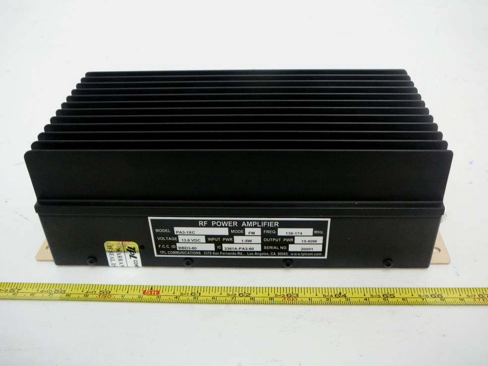
BBD3-60
Oct 09, 2012RF Power Amplifier
Equipment Class
AMP - Amplifier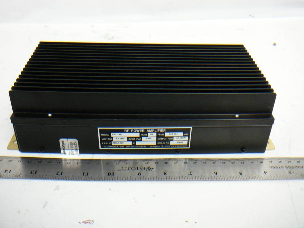
BBD3-125
Oct 01, 2012RF Power Amplifier
Equipment Class
AMP - Amplifier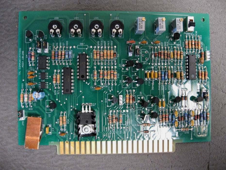
BBDPA9096-350
Oct 27, 2011RF Power Amplifier
Equipment Class
AMP - Amplifier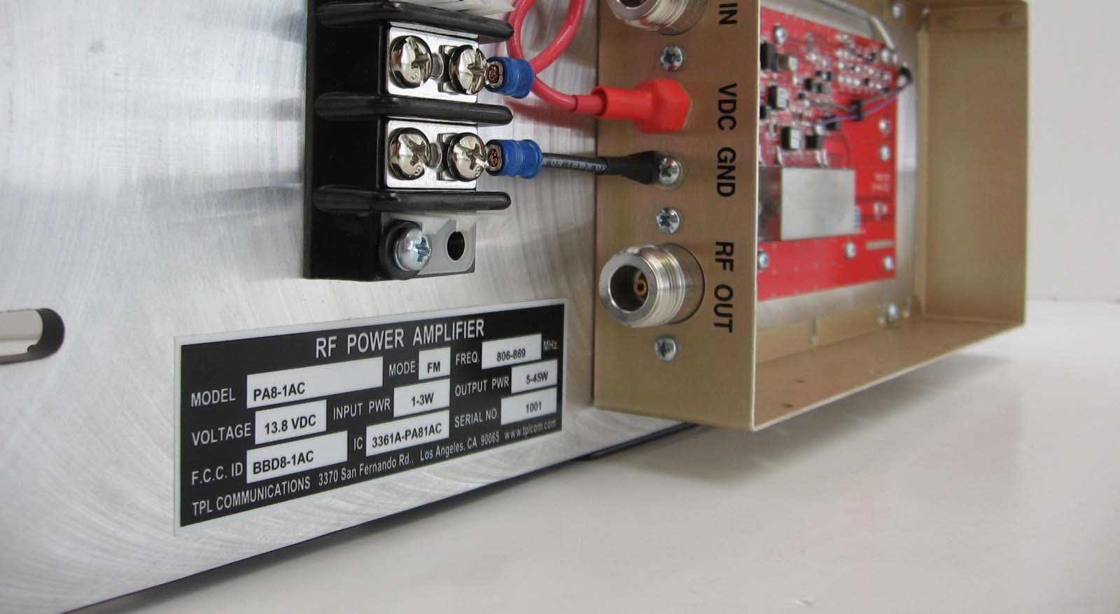
BBD8-1AC
Mar 31, 2010RF Power Amplifier
Equipment Class
AMP - Amplifier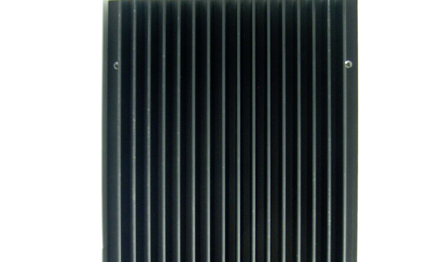
BBD1-1AEL
Aug 13, 2007RF Power Amplifier
Equipment Class
AMP - Amplifier