BJMTWN5213Wireless Webpad
Tatung Company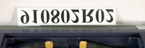
Click to zoom
Application Details
- Equipment Class
- DSS - Part 15 Spread Spectrum Transmitter
- Date of Grant
- Sep 29, 2002
- Application Purpose
- Original Equipment
- Date of Application
- Sep 29, 2002
- Equipment Note
- Wireless Webpad
- Frequency Range
- 2412.00000000 - 2462.00000000
- Company
- Tatung Company
- Country
- Taiwan
Documents & Files
Document Text
Text extracted from the exhibit documents filed with the FCC. Open a document above to read the original.
Users Manual
2002/9/3 page1 TWN-5213CU ViVa1.0 User Guide Revision 1.6 TATUNG WebPAD (TWN-5213CU) User Guide Page 2 Copyright The information contained in this document is provided “as is” and is subject to change without notice. Tatung Company makes no warranty of any kind with regard to this manual, including, but not limited to, the implied warranties of merchantability and fitness for a particular purpose. Tatung Co. shall not be liable for any errors contained herein or for incidental or consequential damages in connection with the furnishing, performance, or use of this manual or the examples herein. © TATUNG Co. 2002. This document contains proprietary information that is protected by copyright. All rights are reserved. No part of this document may be photocopied, reproduced, adapted, or translated to another language without the prior written consent of Tatung Co., except as allowed under the copyright laws. The programs that control this product are copyrighted and all rights are reserved. Reproduction, adaptation, or translation of those programs without prior written permission of Tatung Co. is also prohibited. Tatung is the register trademark of TATUNG Company. Microsoft, Windows CE, ActiveSync, Windows, and the Windows logo are either registered trademarks or trademarks of Microsoft Corporation in the United States and/or other countries. Microsoft products are licensed to OEMs by Microsoft Licensing, Inc., a wholly owned subsidiary of Microsoft Corporation. All other brand names and products names used in this document are trade names, service marks, trademarks, or registered trademarks of their respective owners. Tatung Company 22 Chung-Shan N. Rd., Sec. 3 Taipei, Taiwan 104 R.O.C. TATUNG WebPAD (TWN-5213CU) User Guide Page 3 Messages Messages are used in this manual to bring important information to your attention. Each type of message is defined as below: CAUTION! : Pay Attention! A caution informs you that improper use of equipment or failure to follow safety instructions may cause data loss or damage your equipment. WARNING! : A warning informs you that improper use of equipment or failure to follow safety instructions may cause bodily injury. NOTE! : A note is an advice that helps you to make best use of your TATUNG WebPAD. Safety Instructions The user must read through all safety instructions before using the TATUNG WebPAD (TWN-5213CU). The following information contains concepts that must be fully understood by the user in order to avoid potential hazards that may result in property damage or bodily injury. TATUNG WebPAD (TWN-5213CU) User Guide Page 4 CAUTION! Always use the battery pack that is provided with this WebPAD by TATUNG because other battery packs may have different specifications. Potential hazards and damages may occur to the WebPAD. Do not expose the battery pack to other metal objects. Store it in a cool and dry place. Do not use or place the WebPAD near sources of heat or expose it to direct sunlight for an extended period of time. Do not push or apply force to the TFT screen. Do not use pen or sharp objects to write on the screen. Always use the stylus to tap or draw on the TFT screen. Keep the WebPAD away from liquids to avoid accidental damages to the unit. Avoid exposure to direct lighting. Bright spots may appear on the screen. WARNING! Using worn or damaged power cords may result in electric shock or fire. Avoid keeping one position for long periods of time and also take periodic breaks, in order to prevent any physical discomfort. In addition, take time to exercise your body periodically. If there is a need for repair or adjustment, always contact an authorized TATUNG service provider for assistance. TATUNG WebPAD (TWN-5213CU) User Guide Page 5 Table of Contents 1. Overview........................................................................................ ............................................................7 2. Equipment Checklist .................................................................... ............................................................8 3. System Specification ................................................................... ............................................................9 4. WebPAD Outlook .......................................................................... ............................................................10 4.1 Front View of the WebPAD ................................................................................................................................... 10 4.2 Top View of the WebPAD...................................................................................................................................... 12 4.3 Left View of the WebPAD...................................................................................................................................... 12 4.4 Right View of the WebPAD ................................................................................................................................... 13 4.5 Back View of the WebPAD .................................................................................................................................... 14 5. Quick-Start Procedure ................................................................. ............................................................15 5.1 Starting TATUNG WebPAD .................................................................................................................................. 15 5.2 Booting Logo ......................................................................................................................................................... 17 5.3 Booting Options..................................................................................................................................................... 17 5.4 Changing the Image from the CompactFlash Card ...............................................................................…
Text truncated - open the document above for the full version.
External Photos
Page 1 ANNEX PHOTOGRAPHS OF EUT Page 2 Page 3
ID Label/Location Info
TATUNG WebPAD (TWN-5213CU) User Guide Page 14 4.5 Back View of the WebPAD Battery Connector Cover Battery Pack Battery Latch Battery Release Switch IDE CompactFlash Card Slot Cover Backup Battery and RTC Battery Cover Back Stand / Handle
ID Label/Location Info
S ic herheit geprufte . . T U V R heinla nd . . T U V R heinla nd . . G ruppe s tra hlungs a rm low ra dia tion MP R II IS O 9241-3 E R G O N O MIE G E P R U F T . . E R G O N O MIC S A P P R O V E D WA R N IN G A V IS WA R N U N G . . R IS K O F E L E C T R IC AL S H O C K . DO N O T O P E N . R IS Q U E DE C H O C E L E C T R IQ U E . N E P AS O U V R IR . V O R S IC H T V O R E L E K T R IS C H E M S C H L AG . AB DE C K U N G N IC H T O F F N E N . R E 132236 geprufte S icherheit . . T U V R heinla nd . . T U V R heinla nd G ruppe . . s tra hlungs a rm low ra dia tion MP R II IS O 9241-3 E R G O N O MIE G E P R U F T . . E R G O N O MIC S AP P R O V E D geprufte S icherheit . . T U V R heinla nd . . T U V R heinla nd G ruppe . . s tra hlungs a rm low ra dia tion MP R II IS O 9241-3 E R G O N O MIE G E P R U F T . . E R G O N O MIC S AP P R O V E D R L R 556856 E N E R G IE - S P AR E N D E N E R G Y S A V I N G T U V R heinla nd G ruppe . . s tra hlungs a rm low ra dia tion MP R II IS O 9241-3 T U V R heinla nd G ruppe . . IS O 9241-3 T U V R heinla nd G ruppe . . IS O 9241-3 E R G O N O MIE G E P R U F T . . E R G O N O MIC S AP P R O V E D E N E R G IE - S P AR E N D E N E R G Y S A V I N G HI P OT T U V R heinla nd . . N O . 264 E L E C T R O M A G N E T I C F I E L D S A U T O M A T I C R E D U C E D D I S P L A Y P O W E R D O W N 1 2 3 4 5 6 -0 0 D E R G R U N E P U N K 43483 3862A082 N 119 E 132045 R D E R G R U N E P U N K 43483 I T ' S V E R Y W E L L N A D E I N T A I W A N I T ' S V E R Y W E L L N A D E I N T A I W A N I T ' S V E R Y W E L L N A D E I N T A I W A N 300016 E MI IN S P E C T E D Mfr . N O : 3A 0 Y 002 A U T H O R IZE D by B C IQ MO E A to the following two conditions:(1) This device may not cause harmful interference, and (2) this device must accept any interference received, including interference that may cause undesired operation. This device complies with part15 of the FCC Rules.Operation is subject Input:DC16V 2.5A Model:TWN-5213CU Caution : Web Pad TATUNG CO. MADE IN TAIWAN C SAMPLE US E132236 LISTED ITE R L U subject to the following two conditions:(1) This device may not cause harmful interference, and (2) this device must accept any interference received, including interference that may cause undesired operation. This device complies with part15 of the FCC Rules.Operation is Model:TWN-5213CU Caution : Web Pad TATUNG CO. MADE IN TAIWAN Input:DC16V 2.5A SAMPLE E132236 LISTED ITE C US R geprufte S icherheit . . T U V R heinla nd . . Input:DC16V 2.5A Model:TWN-5213CU Web Pad 4/26 for sample delivery 50 pieces before FCC certification TATUNG CO. subject to the following two conditions:(1) This device may not cause harmful interference, and (2) this device must accept any interference received, including interference that may cause undesired operation. This device complies with part15 of the FCC Rules.Operation is Model:TWN-5213CU Caution : Web PAD TATUNG CO. MADE IN TAIWAN Input:DC16V 2.5A E132236 LISTED ITE C US R 0560 ! geprufte S icherheit . . T U V R heinla nd P roduct S a fety . . SCALE 1:1 , size 78 x 28 R1 x 3 , C3 SCALE 2:1 0805 James ask to revise the TUV logo, please confirm the TWN-5213CU System Label. 0920 RDQA revise the FCC and CE T es ted T o C omply With F C C S ta nda rds F O R H O ME O R O F F IC E U S E F C C ID: B J MT WN 5213 subject to the following two conditions:(1) This device may not cause harmful interference, and (2) this device must accept any interference received, including interference that may cause undesired operation. This device complies with part15 of the FCC Rules.Operation is Model:TWN-5213CU Caution : Web PAD TATUNG CO. MADE IN TAIWAN Input:DC16V 2.5A E132236 LISTED ITE C US R 0560 ! geprufte S icherheit . . T U V R heinla nd P roduct S a fety . . T es ted T o C omply With F C C S ta nda rds F O R H O ME O R O F F IC E U S E F C C ID: B J MT WN 5213 L IS T E D N WG Q 5K 36 F C C ID: B J MC M14U H geprufte S icherheit . . RWTUV THIS DEVICE HAS NOT BEEN APPROVED BY THE FEDERAL COMMUNICATIONS COMMISSION.THIS DEVICE IS NOT AND MAY NOT BE OFFERED FOR SALE OR LEASE OR SOLD OR LEASED UNTIL THE APPROVAL OF THE FCC HAS BEEN OBTAINED.
Internal Photos
Page 4 Page 5 Page 6 Page 7 Page 8 Page 9 Page 10
Operational Description
FCC ID: BJMTWN5213 ADT No.910802R02 Operational Description The transmitter of the EUT (WebPAD) is powered by 16VDC power adapter. The antenna is PCB antenna with MMCX connector. The other instruction, please have a look at the users manual. DSSS Information This device is Direct Sequence Spread Spectrum, the data is mixed by pseudorandom code which is an orthogonal code. The mixed data is digital modulated by BPSK and QPSK technique depends on the data rates. The CCK coding is applied for increasing the data rate, and also the processing gain will be increased. The bit rates are 1,2,5.5,11Mbps, the symbol rates are 1,1,1.375,1.375Mbps, the chip rates are always 11Mbps. So, the Chip/symbol is 11,11,8 and 8 respectively. Although is higher bit rate, the processing gain is lower than 10, but the CCK coding used in higher bit rate will provide 2.2dB coding gain.
RF Exposure Info
FCC ID: BJMTWN5213 ADT No.: 910802R02 FCC TEST REPORT REPORT NO.: RF910802R02 MODEL NO.: TWN-5213** ACCORDING: FCC Guidelines for Human Exposure IEEE C95.1 APPLICANT:TATUNG CO. ADDRESS:22, CHUNGSHAN N. RD., 3 RD SEC., TAIPEI, TAIWAN, R.O.C. ISSUED BY:Advance Data Technology Corporation LAB LOCATION:47 14th Lin, Chiapau Tsun, Linko, Taipei, Taiwan, R.O.C. 0528 ILAC MRA Lab Code: 200102-0 FCC ID: BJMTWN5213 ADT No.: 910802R02 RF Exposure Measurement (Portable Device) 1. Introduction 2.4GHz frequency band is regarded specially as a dangerous band for its heating harmfulness to the human body. That’s why microwave oven is operating in this frequency band. The manufacturer whose product is working in this frequency band is obligatory to prove the harmfulness of his product. In this document, we try to prove the safety of radiation harmfulness to the human body for our product. The limit for Maximum Permissible Exposure (MPE) specified in FCC 1.1310 is followed. The Gain of the antenna used in this product is measured in a Fully Anechoic Chamber (FAC), and the maximum total power input to the antenna is measured. Through the Friis transmission formula and the maximum gain of the antenna, we can calculate the distance, away from the product, where the limit of MPE is reached. 2. RF Exposure Limit According to FCC 1.1310: The criteria listed in the following table shall be used to evaluate the environmental impact of human exposure to radio-frequency (RF) radiation as specified in 1.1307(b). FCC ID: BJMTWN5213 ADT No.: 910802R02 LIMITS FOR MAXIMUM PERMISSIBLE EXPOSURE (MPE) Frequency Range (MHz) Electric Field Strength (V/m) Magnetic Field Strength (A/m) Power Density (mW/cm 2 ) Average Time (minutes) (A)Limits For Occupational / Control Exposures 30-30061.40.1631.06 300-1500......F/3006 1500-100,000......56 (B)Limits For General Population / Uncontrolled Exposure 30-30027.50.0730.230 300-1500......F/150030 1500-100,000......1.030 F = Frequency in MHz 3. Friis Formula Friis transmission formula : Pd = (Pout*G) / (4*pi*r 2 ) where Pd = power density in mW/cm 2 Pout = output power to antenna in mW G = gain of antenna in linear scale Pi = 3.1416 R = distance between observation point and center of the radiator in cm Pd is the limit of MPE, 1 mW/cm 2 . If we know the maximum Gain of the antenna and the total power input to the antenna, through the calculation, we will know the distance r where the MPE limit is reached. Ref. : David K. Cheng, Field and Wave Electromagnetics, Second Edition, Page 640, Eq. (11-133). 4. EUT Operating condition The software provided by Manufacturer enabled the EUT to transmit and receive data at lowest, middle and highest channel individually. FCC ID: BJMTWN5213 ADT No.: 910802R02 5. Test Results 5.1 Antenna Gain The maximum Gain measured in Fully Anechoic Chamber is -2dBi or 0.63 (numeric). 5.2 Output Power Into Antenna & RF Exposure Distance : CHANNEL CHANNEL FREQUENCY (MHz) OUTPUT POWER TO ANTENNA (mW) MINIMUM ALLOWABLE DISTANCE ( r ) FROM SKIN (Centi-Meter) 1241235.891.34 6243737.931.38 11246240.091.42 The minimum allowable distance is very close to the enclosure of the antenna. So, the user has no need to worry about the harmfulness of radiation.
Schematics
55 44 33 22 11 D D C C B B A A TWN-5213 R00C.5_0222 P01-INDEX P16-ISA Conn for Debug P17-BOOT_ROM & SRAMP18-AC97 LM4549P19-Audio Amplifer & connP20-SERIAL_PORTP21-LPC_PC87591&ECP22-P23-CLOCK &FIX HOLEP24-PC87391 FOR FIRP25-TOUCH SCREEN CONTROLP26-BATTERY & CHARGER R00A 05/31 HARRY W.LIAO P27-CONNECTOR P02-BLOCK DIAGRAMP03-SC3200 PCI/ISAP04-SC3200 SDRAM I/FP06-SC3200 TFT LCD I/F & IDEP05-SC3200 POWER&GNDP07-LVDS & BACKLIGHTP08-IDE I/F FOR DEBUGP09-COMPACT FLASHP10-SYSTEM POWERP11-SDRAM OM BOARDP12-USB PORTP13-VGA PORTP14-CARD BUS PCI1420P15-PCI_SLOTX2&TPS2216 P28-NOTE R00B 08/01 HARRY W.LIAOR00C 09/20 HARRY W.LIAOR00C.2 10/19 HARRY W.LIAOR00C.3 12/11 HARRY W.LIAOR00C.4 12/19 HARRY W.LIAOR00C.5 02/22 HARRY W.LIAO TWN-5213 HARRY W.LIAO R00C.5 INDEX A 128 , 22, 2002 星星星星星 TitleSize Document Number Rev Date: Sheet of 55 44 33 22 11 D D C C B B A A STRAP SELECTIONS CLKSEL0CLKSEL1CLKSEL2CLKSEL3 STRAP FUNCTION BOOT16TFT_PRSNT27/25MHZFPCI_MONLPC_ROM PCI BUS PULL-UP'S _______________ SC3200 PCI CLOCK DISTRIBUTION Strap Notes:1) THESE SCHEMATICS ARE FOR THE REV B SILICON2) Leave R-pad for pull-up or pull-down resistors.3) Install pull-up -OR- pull-down to select.4) R's shown for defaults, NL/ = NO LOAD5) For 25/27MHZ strap: the Rev B silicon only supports the 27MHZstrap, so strap must be set as shown. (For Rev. C, pull up)6) For PCICLK0 and PCICLK1: place strap as close to CPU aspossible. Do not add excessive trace length to these clock lines.7) See "SC3200 Strap Option" Application Note for a completedescription. TO COSMONAUTHEADERSBELOW TO STRAPS SC3200 INTERFACES: PCI/SUB-ISA, LPC, AUDIO, DOC, PCI CLOCKS; STRAP OPTIONS, PCI BUSPULL-UPS, COSMONAUT HEADERS DESIGN NOTE:Required pull-up DESIGN NOTE: Locate R- PACKS so that no stubs are made on the PCI bus. DESIGN NOTE: If more PCI clo cks are required, add a low skew buffer such as the ICS 552-01B (www.icst.com). SC 3200 pin: PCICLK, must be connected to one of the ICS 552-01B outputs, with the same length wire as the other PCI clo cks. See the " PCI Clock Considerations" appnote formore details. DESIGN NOTE: See PC I-ISA Mid-Termination AppNote DESIGN NOTE: If needed , connect:COSMOS_SMI# to TFTD5_INIT* (page 4)COSMOS_INTR# to TFTD2_AFD*_DSTRB* (page 4).See Cosmonaut Users Guide. DESIGN NOTE: If moreREQ/GNT pairs areneeded, see the"Request/Grant pairexpansion" appnote DESIGN NOTE: There are no devices that usethe ISA high data byte l ane, so there are no connections to signals SD8-SD15 & BHE#. 266 Mhz 0110CLKSEL [3..0] ECN 1112 TWN-5213 HARRY W.LIAO R00C.5 SC3200 PCI/ISA C 328 , 22, 2002 星星星星星 TitleSize Document Number Rev Date: Sheet of PCICLK0_A CLKCOSMOS CLKLPCCOSMOS SA23SA21SA22SA20SA19 ROMCS# SA18SD4SA22SD3SA16SA23SD6SD7SA19SD1SD2SA21SA17SD5SA20LFRAME#_GPIO37 RD# SA15SA1SA18SA11SA6SA5SA2SA0 SA[0..23] SA8SA4 FRAME# REQ1# SA10SA13SA14SA17SA12SA9SA3SA16 CBE1#_D9CBE2#_D10CBE0#_D8CBE3#_D11PAR_D12STOP#_D15IRDY#_D14TRDY#_D13 IOCHRDY_GPIO19_INTC# INTAXREQ0#INTBXPERR#DEVSEL#_BHE#LOCK#SERR# PCICLK0PCICLK1 PCICLK0PCICLK1 SD0SD2SD6 SD0 SD[0..15] SD4SD3SD1SD5SD7 GNT1# PCICLK1 IRTX_SOUT3 CBE1#_D9 INTBX PCICLK0 IOR#_GPIO14_DOCR#DEVSEL#_BHE#STOP#_D15 LOCK# INTAX USBD2+ SER_RDX ROMCS# USBD2- IOW#_GPIO15_DOCW# REQ0# USBD1+USB_OVCUR# SOUT2 PAR_D12IOCHRDY_GPIO19_INTC#CBE2#_D10 GNT1# USB_PWREN WR# PERR# LAD2_GPIO34 CBE0#_D8 REQ1#GNT0# USBD1- LAD3_GPIO35 IRDY#_D14 IRRX1_SIN3 SERIRQ_GPIO39 FRAME# LDRQ#_GPIO36 RD#TRDY#_D13CBE3#_D11 SERR# LFRAME#_GPIO37 SDATAOUT SDATAIN1 SYNC PCBEEP_GPIO16 BITCLK SYNC SDATAOUT AC97CLK AC97RST# DEVSEL#_BHE# BHE# RI2#_GPIO11_IRQ15 IRDY#_D14LOCK#LDRQ#_GPIO36CLKLPCCOSMOSPAR_D12CLKCOSMOSCBE3#_D11FRAME# GNT0# CBE0#_D8STOP#_D15PERR#PCIRST#CBE2#_D10CBE1#_D9DEVSEL#_BHE#SERR#TRDY#_D13 CTS2#_GPIO08_IDEDREQ1SOUT2SIN2 DTR2#_GPIO06_BOUT2_IDEIOR1# DCD2#_GPIO09_IDEIOW1#RI2#_GPIO11_IRQ15DSR2#_GPIO10_IDEIORDY1RTS2#_GPIO07_IDEDACK1# SER_RDX PAR_D12 SD15SD13 CBE2#_D10 SD9SD11 STOP#_D15 SD12 SD8 SD14 CBE3#_D11CBE0#_D8IRDY#_D14CBE1#_D9TRDY#_D13 SD10 AD7 AD6AD5AD4 AD20 AD0AD30 AD15AD8AD29AD18 AD12 AD31AD27 AD16AD9AD24 AD13 AD1AD18AD20AD21 AD17 AD6 AD22 AD5 AD3AD30AD28AD11 AD4AD28AD22 AD5 AD2AD31 AD12AD14 AD13AD15 AD24 AD6 AD0 AD25 AD3AD26 AD1 AD19 AD10 AD10 AD7 AD21 AD2 AD27 AD4 AD[0..31] AD25AD17 AD26 AD29AD8AD19AD14AD11AD23 AD23AD16AD9 AD3AD2 AD7 AD1 SA7 SA6SA4SA5SA1 SA7 SA2SA3 AD13AD12AD9AD8 SA13SA12SA9SA8 AD20AD19 SA20SA19 SD2SD3SD5SD4SD7SD1SD6SA11 AD26AD27AD29AD28AD31AD25AD30AD11 AD0AD16AD15AD14AD10AD24AD23AD22AD21 SA0SA16SA15SA14SA10SD0SA23SA22 AD18AD17 SA18SA17SA21 LAD1_GPIO33 LAD0_GPIO32LPCPD#_GPIO38 SA7SA8SA6SA13SA2SA3SA10SA11SA12 DEVSEL#_BHE# SA5SA1SA15SA0SA4SA14SA9 GNT0# IOCHRDY_GPIO19_INTC# LPCPD#_GPIO38LAD3_GPIO35 INTAX GNT1#REQ0#SERIRQ_GPIO39LAD2_GPIO34LFRAME#_GPIO37LAD0_GPIO32REQ1#LAD1_GPIO33 INTBX USBD2+ 12 USBD2- 12 USB_PWREN 12 USBD1- 12 USBD1+ 12 USB_OVCUR# 12 AD[0..31] 14 PCIRST# 4,14,17,21,24 LAD0_GPIO32 21,24 LAD2_GPIO34 21,24 LAD3_GPIO35 21,24 LDRQ#_GPIO36 24 LFRAME#_GPIO37 2 1,2 4 SERIRQ_GPIO39 2 1,2 4 SA[0..23] 16,17 PCICLK0_A 23 SD[0..15] 16,17 WR# 16,17IOW#_GPIO15_DOCW# 16IOCHRDY_GPIO19_INTC# 16 SERR# 14 IRDY#_D14 14CBE3#_D11 14DEVSEL#_BHE# 14CBE2#_D10 14TRDY#_D13 14CBE0#_D8 14 REQ1# 14INTAX 14 IOR#_GPIO14_DOCR# 16CBE1#_D9 14 PERR# 14INTBX 14,16 RD# 16,17PAR_D12 14ROMCS# 16,17 GNT1# 14 STOP#_D15 14 BITCLK 18 SDATAIN1 18 SYNC 18 AC97CLK 18 AC97RST# 18 SDATAOUT 18 IRRX1_SIN3 27 IRTX_SOUT3 27 CLKPCI3200 23 RTS2#_GPIO07_IDEDACK1# 20 SOUT2 20 SIN2 20 CTS2#_GPIO08_IDEDREQ1 20 DTR2#_GPIO06_BOUT2_IDEIOR1# 20 RI2#_GPIO11_IRQ15 20 DCD2#_GPIO09_IDEIOW1# 20 DSR2#_GPIO10_IDEIORDY1 20 SER_RDX 25 SER_TDX 25 FRAME# 14 LAD1_GPIO33 21,24 TFTD2 6,7TFTD5 6,7 LPCPD#_GPIO38 24 PCBEEP_GPIO16 18 DTR1X_GPIO18_BKLEN 7 CLK_LPC_391 24 VCC3.3V VCC3.3V VCC3.3V VCC3.3V VCC3.3V T TP291 TEST PAD R24 1.5K_NO_LOAD 1 R15 1.5K_NO_LOAD 1 R9 1.5K_NO_LOAD 1 R12 1.5K 1 RP10 75_16P8R/4016 1 16 2 15 3 14 4 13 5 12 6 11 7 10 8 9 R8 1.5K 1 R14 1.5K 1 R7 1.5K 1 R2 10 1 RP510K_8P4R 1234 5678 R23 1.5K 1 R6 1.5K 1 R1 10_NO_LOAD 1 R743 0_NO_LOAD 1 RP1 10K_8P4R 1234 5678 R17 1.5K …
Text truncated - open the document above for the full version.
Schematics
A A B B C C D D E E 44 33 22 11 128KX8 FLASH128KX16 SRAM CONNECT AGND TO DGND HERE A ANALOG GROUND D DIGITAL GROUND 3.3/5 VOLT LOW VLTAGE KEYED VS1# IOIS16 * ASSERTED DD DD DD D D DDD D D D D DD DIGITAL POWER PLANE LOCATED LOSE TO MAC AND SRAM DIGITAL GROUND TIE ANALOG AND DIGITAL GROUND CLOSE TO CONNECTOR P1 ANALOG/RF POWER PLANE NO POP NO POP NO POP NO POP NO POP AA DD D D NO POP NO POP NVCS* MOE* MWEL* MWEL* MLBE* MWEH_MA0 RAMCS* MOE* N/C HOE* HREG* HIORD* HIOWR* HCE1* HCE2* HINPACK* HIREQ* HSTSCHG* HWAIT* HWE* HRESET AD A (NEAR 3871 PINS) (NEAR 3871 PINS) (NEAR 3871 PINS)(NEAR 3871 PINS) AAA HCE1* HOE* HWE* HIREQ* HCE2* HIORD* HIOWR* HRESET HWAIT* HINPACK* HREG* HSTSCHG* DDD NO POPNO POP NO POPNO POPNO POPNO POPNO POP DD NO POPNO POP 10UF 10UF 10UF 10UF 0.1UF 0.1UF 0.1UF 0.1UF 0.1UF0.1UF0.1UF0.1UF0.1UF0.1UF0.1UF0.1UF0.1UF0.1UF0.1UF0.1UF0.1UF0.1UF0.1UF 0.1UF0.1UF 0.1UF0.1UF0.1UF0.1UF0.1UF0.1UF 0.1UF0.1UF 0.1UF 0.1UF 0.1UF0.1UF0.1UF0.1UF 0.1UF0.1UF 0.1UF 1000PF 1000PF 10PF 220PF 22PF 560NH BLM21P300S BLM21P300S BLM21P300S BLM21P300S BLM21P300S AME8805_5V AME8801_2.8V PCMCIA68PIN CONN. AT24C08A CMR200T 44MHz OSC EM128L16B AM29LV010B ISL3871IK 47K NO POP 0 0 0 10K 10K 1.13K 12.1K 560 1.5K 0 0 NO POP 0 10M 9.53K 19.1K 0.1UF <Doc>B PCMCIA D 12Monday, March 04, 2002 Title SizeDocument NumberRev Date:Sheetof +3.3V RADIO_PE UNNAMED_2_0402RES_I679_B MD[0..15] +3.3V MA16 MA17 MA16 HD[0..15] HATSCHG* LFXTALO SALLY+3.3V +3.3VIN DAVE2 DAVE1 MD1 MD10 MA9 MA12 NVCS* HWE* HWAIT* HA9 NVCS* HD1 HD2 MD3 HD12 RAMCS* HA5 HA2 HA1 HIORD* MD6 HD6 HA4 HCE1* HREG* HA3 HA0 HD9 HD13 HRESET HINPACK* HREG* HD7 HD8 MD6 MOE* HWAIT* MD0 HA0 HD0 HD14 MOE* MA12 MA5 MA3 HOE* HD13 HD12 HD10 HD6 HD7 HD3 HA1 HA2 HINPACK* MD10 HA3 MD2 HCE2* HA7 MA10 MWEL* MA9 MA14 MA15 MA8 HD2 HD3 MD12 MD5 MD3 HIORD* HA7 HA6 HD5 MA12 MA13 MA9 MA4 HCE1* HD0 MA7 MA15 MWEH_MA0 FSADOFF TX_AGC MD0 HIREQ* HD14 HD15 MA8MA6 HA6 MA1 MA11 MA11 MA10 HD10 MA3 MA13 MD12 MD15 MD9 MD13 MD7 MA17 HIOWR* HA8 HA4 HD11 MD7 MD4 MD15 MD5MA14 MA13 MA16 MA10 MA1 HA[0..9] MA7 MA8 HWE* HIREQ* MD3 MD9 HA9 HOE* HD9 MD13 MD11 MD1 MA2 HD4 MD7 HA8 HD4 MD1 HD5 MA5 MD2 MD2 RAMCS* MA2 HCE2* MA11 MA7 HSTSCHG* MD6 HIOWR* MA4 MOE* MA1 HD15 MA5 MD0 MWEH_MA0 MD4 MD4 HD11 MD5 MLBE* MWEH_MA0 MWEL* MA3 MD14 MD14 LFXTALI MWE* HD8 HD1 MD8 MA6 MA4 MD11 MA15 HA5 HRESET MA2 MD8 MLBE* MA6 MA14 +3.3VVCCAVCCSVCCA VCCA VCCS VCCS +3.3V VCCS VCCS VCCS VCCB VCCS +3.3V R55 D100 LEDSMD R9 C4 TP28 1 U13 4 1 2 3 VDD GND GND OUT TP12 1 R10 32.768KHz U4 12 3 12 CASE C21 TP20 1 R3 U9 1 2 3 45 6 7 8 A0 A1 A2 GNDSDA SCL WP VCC TP13 1 TP25 1 TP15 1 C3 D4 LEDSMD R2 P1 1 2 3 4 5 6 7 8 9 10 11 12 13 14 15 16 17 18 19 20 21 22 23 24 25 26 27 28 29 30 31 32 33 34 35 36 37 38 39 40 41 42 43 44 45 46 47 48 49 50 51 52 53 54 55 56 57 58 59 60 61 62 63 64 65 66 67 68 GND1 D3 D4 D5 D6 D7 CE1* A10 OE* A11 A9 A8 A13 A14 WE*/PGM* IREQ* Vcc1 Vpp1 A16 A15 A12 A7 A6 A5 A4 A3 A2 A1 A0 D0 D1 D2 IOIS16* GND2 GND3 CD1* D11 D12 D13 D14 D15 CE2* RFSH IORD* IOWR* A17 A18 A19 A20 A21 Vcc2 Vpp2 A22 A23 A24 A25 VS2 RESET WAIT* INPACK* REG* SPKR* STSCHG* D8 D9 D10 CD2* GND4 TP14 1 C5 C8 R200 TP21 1 C19 U1 F3 G4 G3 H5 H4 H3 H2 D4 C4 C3 B4 B3 A5 A4 A3 B5 B2 D1 D2 C2 C1 B1 G6 F6 F5 E5 E1 E6 H1 H6 E4 F4 A1 G5 A2 D5 C5 C6 B6 G1 F1 F2 E2 D6 G2 E3 D3 A6 A14 A13 A12 A11 A10 A9 A8 A7 A6 A5 A4 A3 A2 A1 A0 CE* UB* VSS I/O11 I/O10 I/O9 I/O8 I/O7 I/O6 I/O5 1/O4 VDD VSS NC NC A16 A15 LB* WE* OE* I/O3 I/O2 I/O1 I/O0 I/O15 I/O14 I/O13 I/O12 VDD NC NC NC NC C51 C9 TP7 1 C14 C46 L17 TP22 1 TP23 1 C74 R15 R14 R22 C52 R13 R12 C49 TP1 1 U5 149 121 119 117 172 171 167 158 160 120 118 116 170 166 159 157 125 126 128 130 134 135 136 137 143 145 173811512314016418092844113132152169192202617275819110557102 147 127 146 144 150 148 129 138 124 133 139 52 1 55 29 32 35 30 31 64 68 65 69 84 94 97 67 85 95 96 107 25 26 24 141 53 54 103 104 16371141221421618274311213115116819120160100596678889910658101 196 195 194 193 190 189 188 187 186 185 184 183 182 181 177 176 175 174 23 22 21 20 19 18 15 14 13 12 11 206 205 204 203 198 7 10 207 208 6 197 73 74 86 87 82 83 79 80 76 77 62 63 71 70 56 40 51 50 48 89 92 93 98 90 36 49 34 39 33 42 41 45 46 47 163 162 165 200 178199 173 5 4 3 2 108 109 110 111 153 154 155 156 179 HD15 HD0 HD1 HD2 HD3 HD4 HD5 HD6 HD7 HD8 HD9 HD10 HD11 HD12 HD13 HD14 HA0 HA1 HA2 HA3 HA4 HA5 HA6 HA7 HA8 HA9 IO_VDDDIO_VDDDIO_VDDDIO_VDDDIO_VDDDIO_VDDDIO_VDDD CORE_VDDDCORE_VDDDCORE_VDDDCORE_VDDDCORE_VDDDCORE_VDDDCORE_VDDDCORE_VDDDCORE_VDDD VDDAVDDAVDDAVDDAVDDA VDDA (PLL) VDDAVDDA HOE* HREG* HIORD* HIOWR* HCE1* HCE2* HINPACK* HIREQ* HSTSCHG* HWAIT* HWE* RESET* DBG0 TESTMODE TCLKIN PJ2 (MISO) PJ6 (LED) PJ0 (SCLK) PJ1 (SD) COMP1Q COMP1I COMP2Q COMP2I COMPIQ COMPRX COMPTX FSADOFF FSADIQ FSADRX FSADTX FILTER CLKIN LFXTALI LFXTAL0 MCLK NC NC NC NC IO_GNDDIO_GNDDIO_GNDDIO_GNDDIO_GNDDIO_GNDDCORE_GNDDCORE_GNDDCORE_GNDDCORE_GNDDCORE_GNDDCORE_GNDDCORE_GNDDCORE_GNDDCORE_GNDDVSUBVSUBVSUBGNDAGNDAGNDAGNDAGNDA (PLL)GNDDGNDD MA1 MA2 MA3 MA4 MA5 MA6 MA7 MA8 MA9 MA10 MA11 MA12 MA13 MA14 MA15 MA16 MA17 MA18 MD0 MD1 MD2 MD3 MD4 MD5 MD6 MD7 MD8 MD9 MD10 MD11 MD12 MD13 MD14 MD15 MOE* MWE* MLBE* NVCS* RAMCS* MWEH_MA0* VREF IREF TXQ+ TXQ- TXI+ TXI- RXQ+ RXQ- RXI+ RXI- QOFFSET- QOFFSET+ IOFFSET+ IOFFSET- VCO_SELECT PK1 (SYNTH_CLK) PL7 (TR_SW) PL3 (TR_SW_BAR) LNA_H/L BBOVLD BBAGC+ BBAGC- TXAGC TXDET PJ7 (RADIO_PE) PK7(CAL_EN) PJ5 (LE_IF) PK0 (LE_RF) PJ4 (PE1) PK4 (PE2) PK2 (SYNTH_DATA) PK3 (PA_PE) ANT_SEL ANT_SEL* USB+ USB- USB_DET IO_VDDD IO_GNDDIO_GNDD PL4 DBG4 DBG3 DBG2 DBG1 TEST0 TEST1 TEST2 TEST3 TEST4 TEST5 TEST6 TEST7 CLKOUT U6 4 2 5 3 1 BP GND OUT SHDN* IN C47 C34 C115 C18 TP2 1 C116 C29 C81 C31 TP3 1 R57 C110 C22 R5 TP4 1 C102 R74 C26 C1 R4 R73 C76 C7 R37R78 L10 C6 R32 U2 10 11 5 4 12 1 31 2 3 13 14 15 16 17 18 19 20 7 30 32 28 27 25 23 22 21 6 9 24 8 26 29 A16 A15 A14 A13 A12 A11 A10 A9 A8 A7 A6 A5 A4 A3 A2 A1 A0 WE* CE* OE* DQ6 DQ5 DQ3 DQ2 DQ1 DQ0 NC NC VSS VCC DQ4 DQ7 TP8 1 R16 R38 L9 TP16 1 R150 R39 C12 L1 R1 C32 R18 TP9 1 R21 C35 C45 R88 TP10 1 C44 TP17 1 C39 U17…
Text truncated - open the document above for the full version.
Test Report
FCC ID: BJMTWN5213 Report No.: RF910802R021Issued: August 21, 2002 FCC TEST REPORT REPORT NO.: RF910802R02 MODEL NO.: TWN-5213** RECEIVED: August 2, 2002 TESTED: June 24 ~ August 2, 2002 APPLICANT:TATUNG CO. ADDRESS:22, CHUNGSHAN N. RD., 3 RD SEC., TAIPEI, TAIWAN, R.O.C. ISSUED BY:Advance Data Technology Corporation LAB LOCATION:47 14th Lin, Chiapau Tsun, Linko, Taipei, Taiwan, R.O.C. This test report consists of 46 pages in total. It may be duplicated completely for legal use with the approval of the applicant. It should not be reproduced except in full, without the written approval of our laboratory. The client should not use it to claim product endorsement by CNLA, NVLAP or any government agencies. The test results in the report only apply to the tested sample. 0528 ILAC MRA Lab Code: 200102-0 FCC ID: BJMTWN5213 Report No.: RF910802R022Issued: August 21, 2002 Table of Contents 1CERTIFICATION...........................................................................................4 2SUMMARY OF TEST RESULTS...................................................................5 3GENERAL INFORMATION............................................................................6 3.1GENERAL DESCRIPTION OF EUT..............................................................6 3.2DESCRIPTION OF TEST MODES................................................................7 3.3GENERAL DESCRIPTION OF APPLIED STANDARDS...............................7 3.4DESCRIPTION OF SUPPORT UNITS..........................................................8 4TEST TYPES AND RESULTS.......................................................................9 4.1CONDUCTED EMISSION MEASUREMENT................................................9 4.1.1LIMITS OF CONDUCTED EMISSION MEASUREMENT..............................9 4.1.2TEST INSTRUMENTS..................................................................................9 4.1.3TEST PROCEDURES.................................................................................10 4.1.4TEST SETUP..............................................................................................10 4.1.5EUT OPERATING CONDITIONS................................................................11 4.1.6TEST RESULTS..........................................................................................12 4.2RADIATED EMISSION MEASUREMENT...................................................18 4.2.1LIMITS OF RADIATED EMISSION MEASUREMENT.................................18 4.2.2TEST INSTRUMENTS................................................................................19 4.2.3TEST PROCEDURES.................................................................................20 4.2.4TEST SETUP..............................................................................................21 4.2.5EUT OPERATING CONDITIONS................................................................21 4.2.6TEST RESULTS..........................................................................................22 4.36dB BANDWIDTH MEASUREMENT...........................................................27 4.3.1LIMITS OF 6dB BANDWIDTH MEASUREMENT........................................27 4.3.2TEST INSTRUMENTS................................................................................27 4.3.3TEST PROCEDURE................................................................................…
Text truncated - open the document above for the full version.
Contact Information
Applicant
Chung Chang(Director)
Technical Contact
Advance Data Technology CorporationVivi Wang
[email protected]+886 3 327 0910
13-1, Lane 19, WenShan 3rd St · Taoyuan · Taiwan
Test Firm
Bureau Veritas CPS (H.K.) Ltd. Taoyuan BranchRichard Chen
Technical Specifications
| # | Rule Parts | Frequency Range | Power Output |
|---|---|---|---|
| 1 | 15C | 2.41 GHz - 2.46 GHz | 40.00 mW |
Other Applications from Tatung Company

BJM-TH1WD
Oct 05, 2021TUF GAMING H1 WIRELESS DONGLE
Equipment Class
DXX - Part 15 Low Power Communication Device Transmitter
BJM-RSGB
Mar 22, 2021Gaming headset
Equipment Class
DTS - Digital Transmission System
BJM-TUFH3WLD
Jan 03, 2021TUF Gaming H3 Wireless dongle
Equipment Class
DXX - Part 15 Low Power Communication Device Transmitter
BJM-TUFH3WL
Dec 23, 2020TUF GAMING H3 WIRELESS
Equipment Class
DXX - Part 15 Low Power Communication Device Transmitter
BJM-TIH-F1500
May 26, 2015Induction Cooker
Equipment Class
8CC - Part 18 Consumer Device