BV2-MPGBR052WIRELESS LAN MINI PCI ADAPTER
D&M Holdings Inc.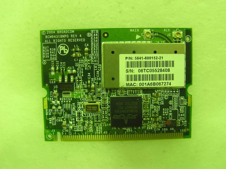
Click to zoom
Application Details
- Equipment Class
- DTS - Digital Transmission System
- Date of Grant
- May 14, 2007
- Application Purpose
- Original Equipment
- Date of Application
- May 13, 2007
- Equipment Note
- WIRELESS LAN MINI PCI ADAPTER
- Frequency Range
- 2412.00000000 - 2462.00000000
- Company
- D&M Holdings Inc.
- Country
- Japan
Documents & Files
Document Text
Text extracted from the exhibit documents filed with the FCC. Open a document above to read the original.
Users Manual
All rights are reserved by USI. No part of this technical document can be reproduced in any form without permission of USI. Data Sheet Sep. 2005 Rev 1.6 MP-G-BR-05, EXT. 2 802.11G 16BIT WIRELESS LAN MINI PCI ADAPTER Introduction The Mini-PCI Adapter type-III B is a high-speed 54 Mbits/s wireless networking card providing a multimode 802.11 b/g or 11g mode only connectivity for enterprise and home wireless LAN access. The Mini-PCI Card uses direct sequence spread spectrum (DSSS), Orthogonal Frequency Division Multiplexing (OFDM) technology, and implements DBPSK, DQPSK, and CCK, OFDM modulation, as defined in the IEEE® 802.11b, g. This gives a very robust radio channel, which is made even better by the excellent receiver sensitivity and delay spread robustness. In environments with radio interference, the Mini-PCI Card, because of its acknowledgment protocol and its option to be tuned to another frequency channel, continues to run. Superior echo path management makes it suitable for areas with a large delay spread, for example, warehouses. This reduces the number of cells required and, therefore, reduces the total cost of ownership. A firmware-based architecture is capable of supporting the latest industry standards in the security and quality of service (QoS), as the draft 802.11i and 802.11e standards, respectively. The Mini-PCI Card is complemented by drivers and networking tools for various versions of the Windows ® operating system. USI provides extensive technical documentation on integration issues such as antenna design, customizing drivers, and management software. Features • Automatic fallback: 54 Mbit/s, 48 Mbit/s, 36 Mbit/s, 24 Mbit/s, 18 Mbit/s, 12 Mbit/s, 11 Mbit/s, 9 Mbit/s, 6 Mbit/s, 5.5 Mbits/s, 2 Mbits/s, or 1 Mbit/s . • Feature with Afterburner technology for this 54g platform, Products with this new technology provide up to 40 percent greater throughput than typical standard 802.11g systems without impacting the performance of neighboring wireless LANs. • Low power consumption. • Automatic power management to reduce battery use. • Easy integration into mobile and hand-held platforms. It’s flexible for design and antenna placement. • External antenna diversity. • Support AES-CCM, WPA (SSN-TKIP), and WEP (64-bit/128-bit or 152-bit). l Corresponding to IEEE 802.11b/gspecification. l Interoperable with other IEEE 802.11a/b/gcompliant systems. l Conformable to industry-standard Mini- PCI Card Type III-B specification. l WDS support l WHQL pre-test and Wi-Fi pre-test. www.usi.com.tw 802.11 b/g Wireless LAN Mini-PCI Adapter All rights are reserved by USI. No part of this technical document can be reproduced in any form without permission of USI. EXECUTIVE SUMMARY This document outlines the product requirements for an 802.11g mini PCI adapter 16 Bits– here after referred as “ MP-G-BR-05 Ext2“.RoHS version This product is targeted for first shipments in Q4, 2005 By using Broadcom chipset solution which including; BCM4318 SoC MAC+BB+Transceiver SiGe SE2521A34 for 11g PA and SE2521A60 as alternative Physical Dimension/Packaging The Mini-PCI Card has been designed to conform to the Mini-PCI specification, as defined in Mini-PCI Specification Rev 0.1. All dimensions in this section have a tolerance as permitted in the Mini-PCI Specification. Dimension: 59.8 mm x 44.8 mm x 5.0 mm (actually Max thickness is 3.3mm on metal shield , there is no component on the bottom side of this card) Weight: Less than 25 g Package: Bulk in 200 pcs. Figure 1. Mini-PCI Type III-B dimension Mechanically unique coaxial connectors for two external antennas. Operating Conditions Operating Temperature 0° to 70° Celsius Operating Humidity 90% (non-condensing) Storage Temperature -10°C to +75°C ambient temperature Storage Humidity 95% (non-condensing) 802.11 b/g Wireless LAN Mini-PCI Adapter All rights are reserved by USI. No part of this technical document can be reproduced in any form without permission of USI. Voltage and Current The MP-G-BR-05 will comply with the following features and standards Voltage 3.3 VDC from host (+/-0.2V) Current 802.11g (Typ.) Transmit <450mA Receive <350mA Stand By <50mA Wireless Specification The MP-G-BR-05 will comply with the following features and standards: Features Description WLAN Standards IEEE 802 Part 11b/g Antenna Connector Hirose connector supported with diversity Data Rates 1, 2, 5.5, 11 Mbps for 802.11b 6, 9, 12, 18, 24, 36, 48, 54 Mbps for 802.11g and 125Mbps for AfterBunrer Medium Access Protocol CSMA/CA (Collision Avoidance) with ACK RF specification Features Description Frequency Band 2412 – 2462 MHz Number of Channels 11 Channels Modulation DBPSK, DQPSK, CCK DSSS for 802.11b & g DPSK, QPSK, 16QAM, 64QAM OFDM for 802.11 g Supported Rates 1, 2, 5.5, 11 Mbps for 802.11b 6, 9, 12, 18, 24, 36, 48, 54 Mbps for 802.11g Maximum Receive Level -20dBm (with PER< 10%) for 802.11g Antenna External (Hirose U-F-L) Typical Output Power 17 dBm for 11b 15 dBm for 11g Note: Actual output power may vary based on manufacturing process variations 802.11g Receive Sensitivity Data Rates Receive Sensitivity 54 Mbps -68 dBm (typ) 11 Mbps -84 dBm (typ.) 6 Mbps -85 dBm (typ.) 1 Mbps -90 dBm (typ.) 802.11 b/g Wireless LAN Mini-PCI Adapter All rights are reserved by USI. No part of this technical document can be reproduced in any form without permission of USI. Note: Actual receive sensitivity for individual products may vary based on manufacturing process and environmental variations Antenna Specifications The Mini-PCI adapter is available in two variants: unique coax connectors with diversity function. On-Board Diversity Switch This variant of the Mini-PCI Card has connectors for two external passive antennas: MAIN and AUX. One of the antennas is used for transmission, and the DSP selects which of the two to use for reception, based on signal strength. The coax connectors for the antennas are mechanically unique, so that no off-the-shelf connector will fit (FCC requirement). Switch ele…
Text truncated - open the document above for the full version.
Cover Letter(s)
D & M Holdings Inc., Denon Brand Company. QualityAssuranceDept. 1-1,Oinokuboyama, Shirakawa, Fukushima 961-0838 Japan Tel : +81-248-27 -3251Fax : +81-248-27 -3280 Letter of Agency April 25, 2007 American Telecommunications Certification Body, Inc. 6731 Whittier Avenue Suite C110 McLean, VA 22101 To Whom It May Concern: Please be advised that D&M Holdings Inc., Denon Brand CompanyauthorizesUL Apex Co., Ltd. to act on our behalf, until otherwise notified, for applications submitted to American Telecommunications Certification Body, Inc. (ATCB). We certify that we are not subject to denial of federal benefits, that includes FCC benefits, pursuant to Section 5301 of the Anti-Drug Abuse ACT of 1988, U.S.C. 862. Further, no party, as defined in 47 CFR 1.2002(b), to the application is subject to denial of federal benefits, that includes FCC benefits. Thank you for your attention to this matter. _________________________________ Kazuhiko Kumagai Chief Engineer, Quality Assurance Dept. D&M Holdings Inc., Denon Brand Company D & M Holdings Inc., Denon Brand Company. QualityAssuranceDept. 1-1,Oinokuboyama, Shirakawa, Fukushima 961-0838 Japan Tel : +81-248-27 -3251Fax : +81-248-27 -3280 FCC Labeling Requirements and Information April 25, 2007 American Telecommunications Certification Body, Inc. 6731 Whittier Avenue Suite C110 McLean, VA 22101 RE: FCC Labeling Requirements FCC ID: BV2-MPGBR052 The following label information is required by the FCC Rules and Regulations for certified devices. Also attached, please find marketing information required by the FCC Rules and Regulations. Thank you for your attention to these matters. Sincerely, _________________________________ Kazuhiko Kumagai Chief Engineer, Quality Assurance Dept. D&M Holdings Inc.,Denon Brand Company D & M Holdings Inc., Denon Brand Company. QualityAssuranceDept. 1-1,Oinokuboyama, Shirakawa, Fukushima 961-0838 Japan Tel : +81-248-27 -3251Fax : +81-248-27 -3280 Request for Confidentiality April 25, 2007 American Telecommunications Certification Body, Inc. 6731 Whittier Avenue Suite C110 McLean, VA 22101 RE: Certification Application FCC ID: BV2-MPGBR052 Please be advised that the following information is to be held confidential on behalf ofD&M Holdings Inc., Denon Brand Company:, referringto the FCC rules 0.457 and 0.459: Theory of Operation Schematics Block Diagram The application contains technicalinformation which D&M Holdings Inc., Denon Brand Company deems to be trade secrets and proprietary. If made public, the information might be used to the disadvantage of the applicant in the market place. Thank you for your attention to this matter. _________________________________ Kazuhiko Kumagai Chief Engineer, Quality Assurance Dept. D&M Holdings Inc., Denon Brand Company D & M Holdings Inc., Denon Brand Company. QualityAssuranceDept. 1-1,Oinokuboyama, Shirakawa, Fukushima 961-0838 Japan Tel : +81-248-27 -3251Fax : +81-248-27 -3280 Manufacturer’s Letter April 25, 2007 American Telecommunications Certification Body, Inc. 6731 Whittier Avenue Suite C110 McLean, VA 22101 RE: Certification Application FCC ID: BV2-MPGBR052 To Whom It May Concern: Please be advised that the manufacturer will ensure that the above-referenced model will be manufactured in accordance with the FCC Rules and Regulations. Thank you for your attention to this matter. _________________________________ Kazuhiko Kumagai Chief Engineer, Quality Assurance Dept. D&M Holdings Inc., Denon Brand Company
Cover Letter(s)
American Telecommunications Certification Body Inc. 6731 Whittier Ave, McLean, VA 22101 May 1, 2007 RE: FCC ID: BV2-MPGBR052_ATCB004854 Attention: Mr Kazufumi Nakai I have a few comments on this Application. Please note that further comments may arise in response to answers provided to the questions below. 1. Please note that as this is a WLAN type device operating in the 2412-2462MHz range and not a Frequency Hopping device the equipment code on the 731 should be DTS and not DSS. Please correct. 2. Please complete page 1 of the Annex A rf technical brief form. Please include the calculated or measured MPE of the device. 3. Please explain how the label is permanently affixed to the device. 4. Please note that the device does not appear to have its own power regulation but instead gets regulated power from a PCI bus. This then would be an LMA and not a full modular approval. Please explain how this meets requirement 3 of DA001407. If the device does in fact get regulated power from a PCI bus and does not have its own DC regulated power on the module, please correct the request to be for an LMA. Please also then either provide testing inside a representative host or please provide some form of attestation to show that the DC regulator used in any host of the companies listed in the manual for which the LMA is to be used will have properly regulated power. 5. Please provide a separate MPE report for this device. Dennis Ward mailto:[email protected] The items indicated above must be submitted before processing can continue on the above referenced application. Failure to provide the requested information may result in application termination. Correspondence should be considered part of the permanent submission and may be viewed from the Internet after a Grant of Equipment Authorization is issued. Please do not respond to this correspondence using the email reply button. In order for your response to be processed expeditiously, you must submit your documents through the AmericanTCB.com website. Also, please note that partial responses increase processing time and should not be submitted. Any questions about the content of this correspondence should be directed to the sender.
Cover Letter(s)
Date: May 9, 2007 FCC ID : BV2-MPGBR052 IC Number : 6963A-MPGBR052 Model : MP-G-BR-05 Ext.2 Applicant : D&M Holdings Inc., Denon Brand Company Request for Limited Modular Approval This modular transmitter will be equipped and used in Audio System. The modular transmitter complies the module basic requirement (Item 1 to 8) in FCC Public Notice: Part 15 Unlicensed Modular Transmitter Approval (DA00-1407) as indicated below. [Module basic requirement] (1) Have its own RF shielding: This modular transmitter has it own RF shielding. Please refer to the following Photo. (2) The modular transmitter must have buffered modulation/data inputs: Data input to this modular transmitter is controlled as not generating excessive data speed and abnormal modulation. (3) The modular transmitter must have its own power supply regulation: The host that has a regulator (PQ070XZ01ZxH or BAXXDD0WHFP, or similarly specification regulator) through the PCI Bus supplies the stable voltage (DC 3.3V). (4) The modular transmitter must comply with the antenna requirements of Section 15.203 and 15.204(c): The antenna of this equipment is connected to the modular antenna with UFL connector, and the installation is to be done by the professionals. There, the equipment complies with the antenna requirement of 15.203 and 15.204(c). (5) The modular transmitter must be tested in a stand alone: The test has been performed as a stand alone. Please refer to the Test Report. (6) The modular transmitter must be labeled with its own FCC ID/ IC Number, and, if the FCC ID/ IC Number are not visible when the module is installed inside another device, then the outside of the device into which the module is installed must also display a label referring to the enclosed module: This modular transmitter is complied with this requirement. Please refer to the Label drawing and location. In addition, the final product will display FCC ID/ IC Number of the module. (7) The modular transmitter must comply with any specific rule or operating requirements applicable to the transmitter and the manufacturer must provide adequate instructions along with the module to explain any such requirements: The necessary explanation to be complied with this requirement is contained in the manual. (8) The modular transmitter must comply with any applicable RF exposure requirements: the mobile. Please refer to the RF Exposure Statement. (No.27HE0375-HO-A, 27HE0375-HO-B) Kazuhiko Kumagai Chief Engineer
Cover Letter(s)
Appendix Appendix1-Rev1.1 The products listed in this document are designed to be used with ordinary electronic equipment or devices (such as audio visual equipment, office-automation equipment, communications devices, electrical appliances and electronic toys). Should you intend to use these products with equipment or devices which require an extremely high level of reliability and the malfunction of with would directly endanger human life (such as medical instruments, transportation equipment, aerospace machinery, nuclear-reactor controllers, fuel controllers and other safety devices), please be sure to consult with our sales representative in advance. Notes No technical content pages of this document may be reproduced in any form or transmitted by any means without prior permission of ROHM CO.,LTD. The contents described herein are subject to change without notice. The specifications for the product described in this document are for reference only. Upon actual use, therefore, please request that specifications to be separately delivered. Application circuit diagrams and circuit constants contained herein are shown as examples of standard use and operation. Please pay careful attention to the peripheral conditions when designing circuits and deciding upon circuit constants in the set. Any data, including, but not limited to application circuit diagrams information, described herein are intended only as illustrations of such devices and not as the specifications for such devices. ROHM CO.,LTD. disclaims any warranty that any use of such devices shall be free from infringement of any third party's intellectual property rights or other proprietary rights, and further, assumes no liability of whatsoever nature in the event of any such infringement, or arising from or connected with or related to the use of such devices. Upon the sale of any such devices, other than for buyer's right to use such devices itself, resell or otherwise dispose of the same, no express or implied right or license to practice or commercially exploit any intellectual property rights or other proprietary rights owned or controlled by ROHM CO., LTD. is granted to any such buyer. Products listed in this document are no antiradiation design. About Export Control Order in Japan Products described herein are the objects of controlled goods in Annex 1 (Item 16) of Export Trade Control Order in Japan. In case of export from Japan, please confirm if it applies to "objective" criteria or an "informed" (by MITI clause) on the basis of "catch all controls for Non-Proliferation of Weapons of Mass Destruction. Contact us Attached-1 Thank you for your accessing to ROHM product informations. More detail product informations and catalogs are available, please contact your nearest sales office. Please contact our sales offices for details ; Japan / (Internal Sales) (Contact address for overseas customers in Japan) U.S.A / San Diego Atlanta Dallas TEL : +1(858)625-3630FAX : +1(858)625-3670 TEL : +1(770)754-5972FAX : +1(770)754-0691 TEL : +1(972)312-8818FAX : +1(972)312-0330 Taiwan / Taipei TEL : +866(2)2500-6956FAX : +866(2)2503-2869 Korea / Seoul TEL : +82(2)8182-700FAX : +82(2)8182-715 Singapore TEL : +65-6332-2322FAX : +65-6332-5662 Malaysia / Kuala Lumpur TEL : +60(3)7958-8355FAX : +60(3)7958-8377 Philippines / Manila TEL : +63(2)807-6872FAX : +63(2)809-1422 Thailand / Bangkok TEL : +66(2)254-4890FAX : +66(2)256-6334 Germany / Dusseldorf TEL : +49(2154)9210FAX : +49(2154)921400 United Kingdom / London TEL : +44(1)908-282-666FAX : +44(1)908-282-528 France / Paris TEL : +33(0)1 56 97 30 60FAX : +33(0) 1 56 97 30 80 China / Hong Kong TEL : +852(2)740-6262FAX : +852(2)375-8971 Shanghai TEL : +86(21)6279-2727FAX : +86(21)6247-2066 Dilian TEL : +86(411)8230-8549FAX : +86(411)8230-8537 Beijing TEL : +86(10)8525-2483FAX : +86(10)8525-2489 As of 18th. April 2005 Tokyo 2-1-1, Yaesu, Chuo-ku, Tokyo 104-0082 TEL : +81(3)5203-0321FAX : +81(3)5203-0300 Yokohama TEL : +81(45)476-2131FAX : +81(45)476-2128 Nagoya Dainagayo Building 9F 3-28-12, Meieki, Nakamura-ku, Nagoya,Aichi 450-0002 TEL : +81(52)581-8521FAX : +81(52)561-2173 Kyoto 579-32 Higashi Shiokouji-cho, Karasuma Nishi-iru, Shiokoujidori, Shimogyo-ku, Kyoto 600-8216 TEL : +81(75)311-2121FAX : +81(75)314-6559 2-4-8, Shin Yokohama, Kohoku-ku, Yokohama, Kanagawa 222-8575 FAX : +81(045)476-9271TEL : +81(45)476-9270 Yokohama
Cover Letter(s)
1 Notice The content of data sheet is subject to change without prior notice. In the absence of confirmation by device specification sheets, SHARP takes no responsibility for any defects that may occur in equipment using any SHARP devices shown in catalogs, data books, etc. Contact SHARP in order to obtain the latest device specification sheets before using any SHARP device. ■ Features Outline Dimensions Lead finish:Lead-free solder plating (Composition: Sn2Cu) Applications Product mass:(0.3g) (Unit : mm) Sheet No.: OP06019 Model Line-up Absolute Maximum Ratings Specific IC Epoxy resin ( ) : Typical dimensions Low Voltage Operation Low Power-loss Voltage Regulator 1.Peripheral equipment of personal computers 2.Power supplies for various electronic equipment such as DVD player or STB Taping Sleeve Package type Output current (I O) 0.5 +0.2 –0.1 (0.5) (1.7) (0.9) (0.5) (0~0.25) 6.6 MAX. 9.7 MAX. 5.5 ± 0.5 2.5 MIN. 5.2 ±0.5 2.3 ±0.5 4–(1.27) 070XZ5M 3 12345 1 2 3 4 5 1 2 3 4 5 DC input (VIN) ON/OFF control (V C) DC output (V O) Output adjustment (V ADJ) GND PQ070XZ5MZxH/PQ070XZ01ZxH PQ070XZ5MZxH PQ070XZ01ZxH 1.Low voltage operation (Minimum operating voltage: 2.35V) 2.5V input → available 1.5 to 1.8V 2.Low dissipation current Dissipation current at no load: MAX.2mA Output OFF-state dissipation current: MAX.5μA 3.Low power-loss (Dropout voltage: MAX.0.5V) 4.Built-in overcurrent and overheat protection functions 5.RoHS directive compliant 0.5A PQ070XZ5MZPH PQ070XZ5MZZH PQ070XZ01ZPH PQ070XZ01ZZH 1A Variable output Taping Sleeve PQ070XZ5MZxH PQ070XZ01ZxH 1 ParameterSymbolRatingUnit 0.5 V VInput voltage 8W °C Power dissipation *1 *3 *2 Junction temperature150 Operating temperature -40 to +85 Storage temperature-40 to +150 Soldering temperature260(10s) 10 (Ta=25°C) Output current *1 °C °C °C *1 All are open except GND and applicable terminals. *2 PD:With infinite heat sink *3 Overheat protection may operate at Tj:125°C to 150°C VIN 10 A ON/OFF control terminal voltage VC Tsol Tstg Topr Tj PD IO Output adjustment terminal voltage *1 VADJ 5 V H Lead finish identification mark 2 Sheet No.: OP06019 Electrical Characteristics V Parameter Output voltage Load regulation Line regulation Ripple rejection - SymbolConditions MIN.MAX.Unit - 0.22.0 - - - Input voltage - % - - 1 TYP. V % - - VIN VO RegL I O=5mA to 0.5A R egI Temperature coefficient of reference voltage 0.2 2.35 - 10 1.5 - 7 1.0 Refer to Fig.2dB - Fig.1 Test Circuit Fig.2 Test Circuit for Ripple Rejection RR 4560 V % 2.0 200 V V1.275 V mA V IN=4 to 8V,IO=5mA T CVrefTj=0 to 125°C, IO=5mA V I-O VC(ON) I C(ON) VC(OFF) IC(OFF) Iqs μA VC=0.4V I O=0mA I O=0mA, VC=0.4V V IN=2.85V,IO=0.3A V ref1.225 ±1.0 I O=0AIq Dropout voltage 0.5 Reference voltage - ON-state voltage for control OFF-state voltage for control OFF-state current for control Output OFF-state consumption current ON-state current for control Quiescent current 4 - -- 0.8 -- 2μA -- 2 - 5μA -- 4 In case of opening control terminal ② , output voltage turns off. + A A A 3 4 5 2 1 V V ei eo 2.7V + + 3 1 2 4 5 V ~ ~ VO=Vref×(1+R2/R1) [R1=1kΩ,Vref≒1.25V] f=120Hz sine wave ei(rms)=0.5V V O=3V(R1=1kΩ) V IN=5V I O=0.3A RR=20log(ei(rms)/eo(rms)) VIN 0.33μF V C IC Iq R2 Vref R1 1kΩ 47μF V O IO RL VIN 0.33μF VC R2 Vref R1 1kΩ 47μF R L IO PQ070XZ5MZxH PQ070XZ01ZxH (Unless otherwise specified, condition shall be VIN=5V, VO=3V(R1=1kΩ), IO=0.3A, VC=2.7V,Ta=25 ̊C,(PQ070XZ5MZxH)) (Unless otherwise specified, condition shall be V IN=5V, VO=3V(R1=1kΩ), IO=0.5A, VC=2.7V,Ta=25 ̊C,(PQ070XZ01ZxH)) IO=5mA to 1.0A PQ070XZ5MZxH PQ070XZ01ZxH VIN=2.85V,IO=0.5A 1.25 4 PQ070XZ5MZxH/PQ070XZ01ZxH + + 3 Sheet No.: OP06019 Ambient temperature Ta (°C) Output voltage V O (V) -40 -20 020 40 60 80 100 120 140 150 0 5 8 10 PD : With infinite heat sink Fig.3 Power Dissipation vs. Ambient Temperature Note) Oblique line portion:Overheat protection may operate in this area. Power dissipation P D (W) Fig.4 Overcurrent Protection Characteristics (PQ070XZ01ZxH) Output current IO (A) Fig.6 Reference Voltage vs. Ambient Temperature PQ070XZ5MZxH/PQ070XZ01ZxH 0 0.5 1 1.5 2 2.5 3 00.511.52 VIN=7V VIN=5V VIN=4.5V VO=3V VIN=10V VIN=5.5V 0 0.5 1 1.5 2 2.5 3 00.20.40.60.811.20.10.30.50.70.91.1 VIN=5V VIN=7V VO=3V VIN=5.5V VIN=4.5V VIN=10V 1.23 1.235 1.24 1.245 1.25 1.255 1.26 -50-25 0255075100 125 VIN=4V V C=2.7V R 1=1kΩ R2=1.4kΩ PQ070XZ01ZxH:IO=0.5A PQ070XZ5MZxH:IO=0.3A Fig.5 Overcurrent Protection Characteristics (PQ070XZ5MZxH) Output voltage V O (V) Output current IO (A) Reference voltage V ref (V) Ambient temperature Ta (°C) 0 0.5 1 1.5 2 2.5 3 3.5 012345 R L =6 Ω O =0.5A ) VC=2.7V T a=Room temp. R1=1kΩ R2=1.4kΩ (VO=3V) C IN=0.33μF C O =47μF RL=10Ω (IO=0.3A) 0.5 1 1.5 2 2.5 3 3.5 012345 VC=2.7V Ta=Room temp. R1=1kΩ R2=1.4kΩ (VO=3V) C IN=0.33μF C O=47μF RL=3Ω (IO=1A) RL=6Ω (IO=0.5A) RL=∞Ω (IO=0.3A) RL=∞Ω(IO=0A) Fig.7 Output Voltage vs. Input Voltage (PQ070XZ5MZxH) Input voltage VIN (V) Output voltage V O (V) I Fig.8 Output Voltage vs. Input Voltage (PQ070XZ01ZxH) Input voltage VIN (V) Output voltage V O (V) 4 Sheet No.: OP06019 PQ070XZ5MZxH/PQ070XZ01ZxH Ambient temperature Ta (°C) 0 10 20 012345 RL=10Ω (IO=0.3A) RL=6Ω (IO=0.5A) VC=2.7V T a =Room temp. R1=1kΩ R2=1.4kΩ (VO=3V) C IN=0.33μF C O=47μF 0 10 20 30 012345 RL=3Ω (IO=1A) RL=6Ω (IO=0.5A) RL= (IO=0A) VC=2.7V Ta=Room temp. R1=1kΩ R2=1.4kΩ (VO=3V) C IN=0.33μF C O=47μF RL=∞Ω(IO=0A) ∞Ω Input voltage VIN(V) Fig.9 Circuit Operating Current vs. Input Voltage (PQ070XZ5MZxH) Circuit operating current I BIAS (mA) Input voltage VIN(V) Fig.10 Circuit Operating Current vs. Input Voltage (PQ070XZ01ZxH) Circuit operating current I BIAS (mA) 0 0.05 0.1 0.15 0.2 0.25 -50-250255075100 125 VIN=2.35V V C=2.7V R 1=1kΩ R2=1.4kΩ (VO=3V) PQ070XZ01ZxH:IO=0.5A PQ070XZ5MZxH:IO=0.3A -50-250255075100 125 0 0.2 0.4 0.6 0.8 1 1.2 1.4 VIN=4V I O=0A V C=2.7V R 1=1kΩ R2=1.4kΩ (VO=3V) PQ070XZ01ZxH PQ070XZ5MZxH Fig.11 Dropout Voltage vs. Junction Temperature Dropout voltage V I-O (V) Ambient temperature Ta (°C) Fig.12 Quiesc…
Text truncated - open the document above for the full version.
External Photos
D&M Holdings Inc., Denon Brand Company Wireless LAN Module Model: MP-G-BR-05 Ext. 2 External Photo PWB Side A with Shield PWB Side B D&M Holdings Inc., Denon Brand Company Wireless LAN Module Model: MP-G-BR-05 Ext. 2 External Photo Antenna
ID Label/Location Info
ID Label Label location Label drawing FCC ID: BV2-MPGBR052 IC: 6963A-MPGBR052
Internal Photos
D&M Holdings Inc., Denon Brand Company Wireless LAN Module Model: MP-G-BR-05 Ext. 2 Internal Photo PWB Side A without Shield
RF Exposure Info
UL Apex Co., Ltd. Head Office EMC Lab. 4383-326 Asama-cho, Ise-shi, Mie-ken 516-0021 JAPAN Telephone : +81 596 24 8116 Facsimile : +81 596 24 8124 Applicant: D&M Holdings Inc., Denon Brand Company Type of Equipment : WLAN Mini PCI card Module Model No. : MP-G-BR-05 Ext.2 FCC ID: BV2-MPGBR052 D&M Holdings Inc., Denon Brand Company declares that Model : MP-G-BR-05 Ext.2 ⇒ complies with FCC radiation exposure requirement specified in the FCC Rules 2.1093(for portable)/2.1091 (for mobile). The “MP-G-BR-05 Ext.2“ has 284.45 mW of conducted Peak Output power and 450.82 mW of EIRP. This kind of equipment is below 60/frequency[GHz] mW(TCB Exclusion List) so that SAR testing is excluded. The Following calculation is the reference data for 20cm distance. RF Exposure Calculations: ← The following information provides the minimum separation distance for the highest gain antenna provided with the “MP-G-BR-05 Ext.2“ as calculate d from FCC OET Bulletin 65 Appendix A, Table (B) Limits for General Population / Uncontrolled Exposure. This calculation is based on the highest EIRP possible from the system, considering maximum power and antenna gain, and considering a 1.0mW/cm^2 uncontrolled exposure limit. The Friis formula used was: S = (P * G) / (4* π * r 2 ) Where P = 284.45 mW (Maximum peak output power) G = 1.58 Numerical Antenna gain; equal 2.00 dBi r =20.0 cm For: MP-G-BR-05 Ext.2S = 0.08969mW/cm 2 No. : 27HE0375-HO RF Exposure / MPE Calculation
Test Report
Test report No. : 27HE0375-HO-A Page : 2 of 59 Issued date : April 19, 2007 FCC ID : BV2-MPGBR052 UL Apex Co., Ltd. Head Office EMC Lab. 4383-326 Asama-cho, Ise-shi, Mie-ken 516-0021 JAPAN Telephone : +81 596 24 8116 Facsimile : +81 596 24 8124 MF060b(14.06.06) CONTENTS PAGE SECTION 1: Client information ............................................................................................................ 3 SECTION 2: Equipment under test (E.U.T.)........................................................................................ 3 SECTION 3: Test specification, procedures & results......................................................................... 4 SECTION 4: Operation of E.U.T. during testing .................................................................................7 SECTION 5: Conducted Emission....................................................................................................... 10 SECTION 6: Spurious Emission.......................................................................................................... 11 SECTION 7: Bandwidth ....................................................................................................................... 12 SECTION 8: Maximum Peak Output Power ..................................................................................... 12 SECTION 9: Peak Power Density........................................................................................................ 12 APPENDIX 1: Photographs of test setup ............................................................................................ 13 Conducted Emission ........................................................................................................13 Spurious Emission (Radiated) ........................................................................................14 Worst Case Position (Horizontal: X-axis/ Vertical:Y-axis) .........................................15 APPENDIX 2: Data of EMI test............................................................................................................ 16 Conducted Emission ........................................................................................................16 6dB Bandwidth.................................................................................................................24 Maximum Peak Output Power.......................................................................................26 Radiated Spurious Emission (below 1GHz) ..................................................................28 Radiated Spurious Emission (above 1GHz) ..................................................................36 Conducted Spurious Emission........................................................................................44 Conducted emission Band Edge compliance .................................................................52 Power Density...................................................................................................................53 99%Occupied Bandwidth ...............................................................................................56 APPENDIX 3:Test instruments ............................................................................................................ 58 Test report No. : 27HE0375-HO-A Page : 3 of 59 Issued date : April 19, 2007 FCC ID : BV2-MPGBR052 UL Apex Co., Ltd. Head Office EMC Lab. 4383-326 Asama-cho, Ise-shi, Mie-ken 516-0021 JAPAN Telephone : +81 596 24 8116 Facsimile :…
Text truncated - open the document above for the full version.
Contact Information
Applicant
Akihiro Yoshida(Professional)
Test Firm
UL Japan, Inc. Yokowa EMC Lab.Masamichi Ishii
Technical Specifications
| # | Rule Parts | Frequency Range | Power Output |
|---|---|---|---|
| 1 | 15C | 2.41 GHz - 2.46 GHz | 284.00 mW |
Other Applications from D&M Holdings Inc.

BV2-DHT-S218
Jan 04, 2024SOUND BAR
Equipment Class
DTS - Digital Transmission System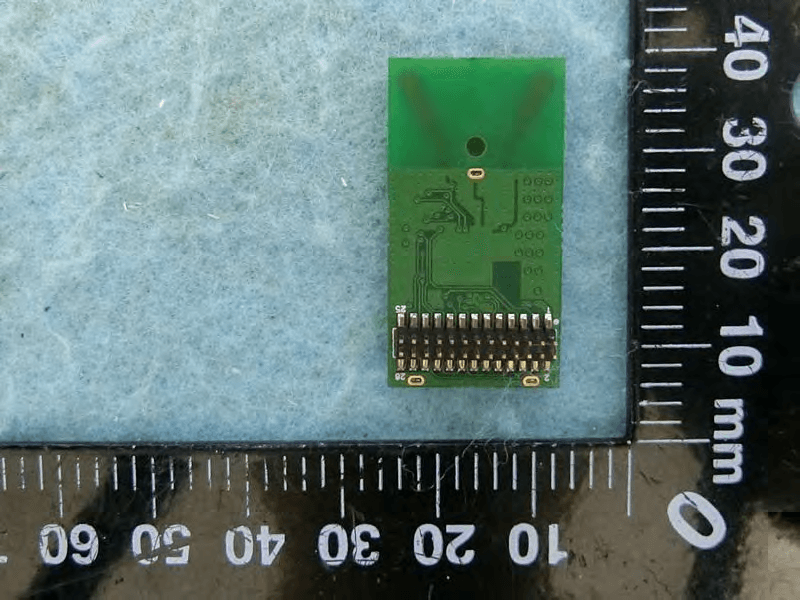
BV2-EW21DM
Jul 06, 2020DENON Wireless Module 5G
Equipment Class
NII - Unlicensed National Information Infrastructure TX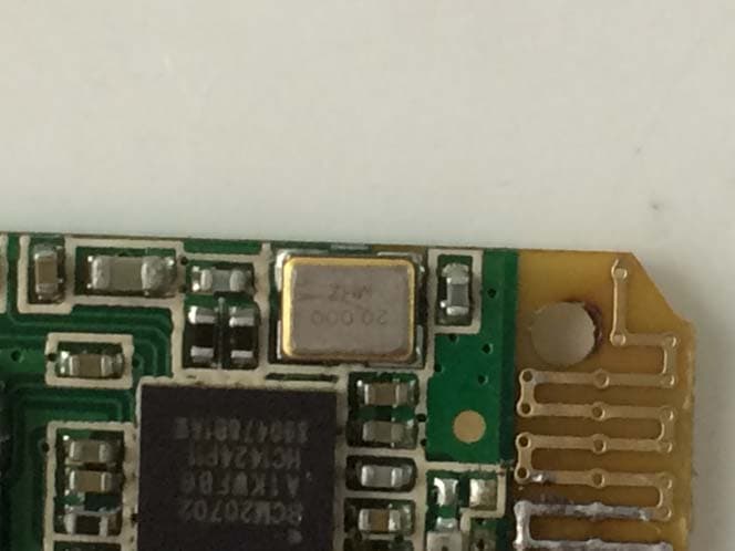
BV2H1GPDONGLE
Apr 01, 2015Bluetooth Dongle
Equipment Class
JBP - Part 15 Class B Computing Device Peripheral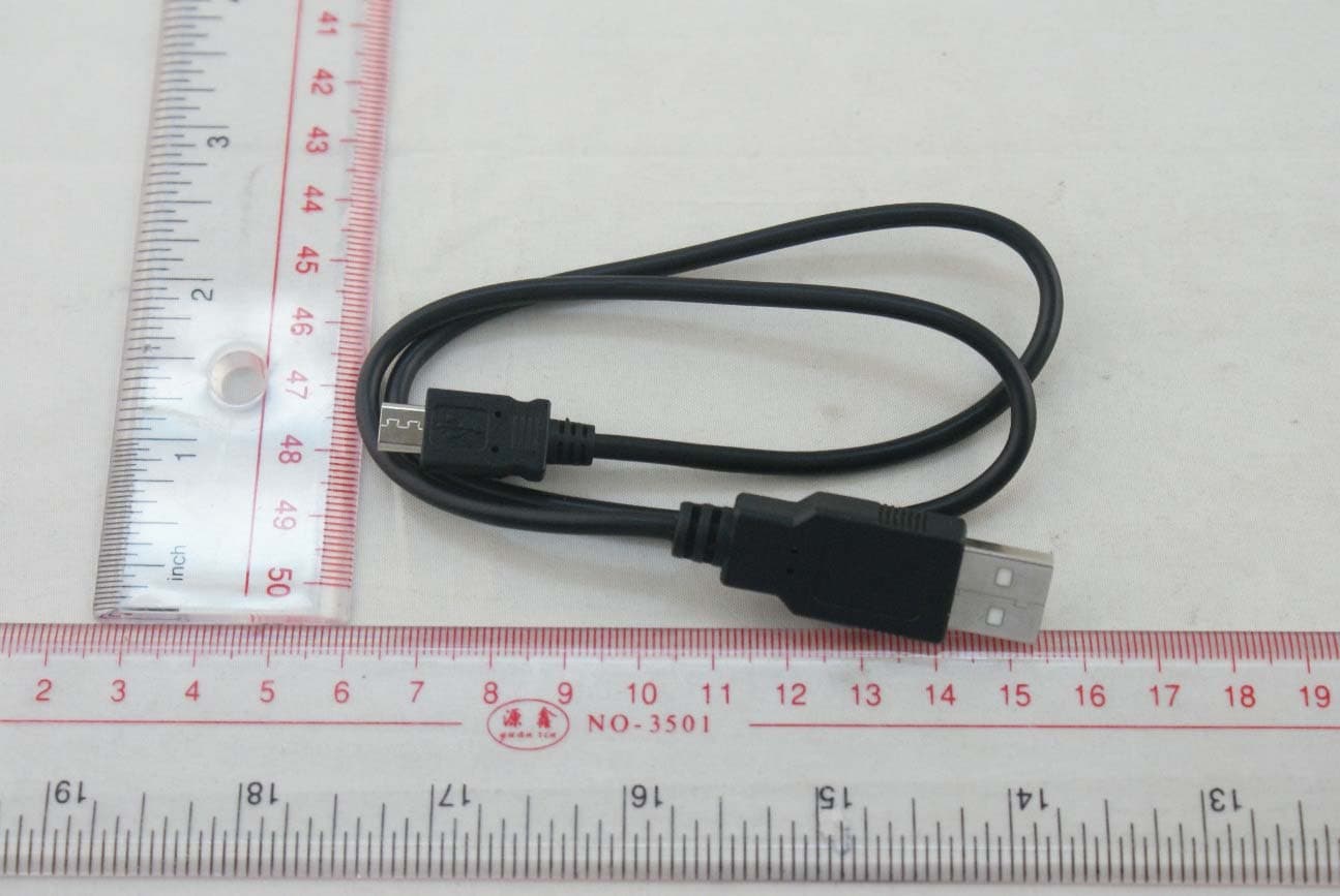
BV2-AHGC20
Dec 18, 2014Bluetooth Headphone
Equipment Class
DSS - Part 15 Spread Spectrum Transmitter
BV2-AH-W200EM
Sep 04, 2013Bluetooth Headphones
Equipment Class
DSS - Part 15 Spread Spectrum Transmitter