BVCDEACSTPAccessory, label deactivator
Tyco Safety Products/Sensormatic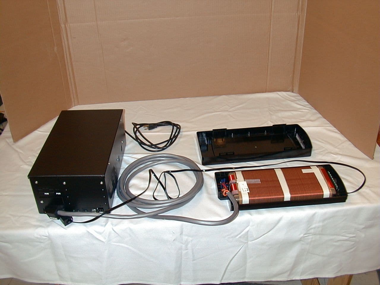
Click to zoom
Application Details
- Equipment Class
- FAP - Part 15 Anti-Pilferage Device
- Date of Grant
- Feb 15, 1999
- Application Purpose
- Original Equipment
- Date of Application
- Dec 15, 1998
- Equipment Note
- Accessory, label deactivator
- Frequency Range
- 0.05800000 - 0.05800000
- Country
- United States
Documents & Files
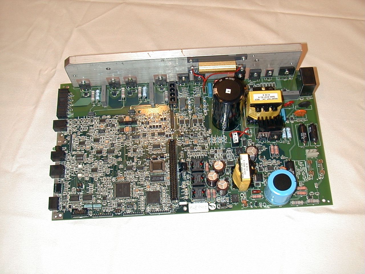
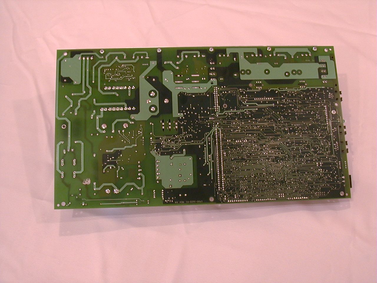
Document Text
Text extracted from the exhibit documents filed with the FCC. Open a document above to read the original.
Users Manual
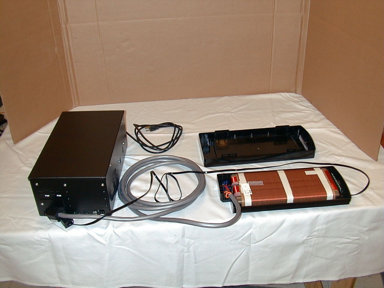
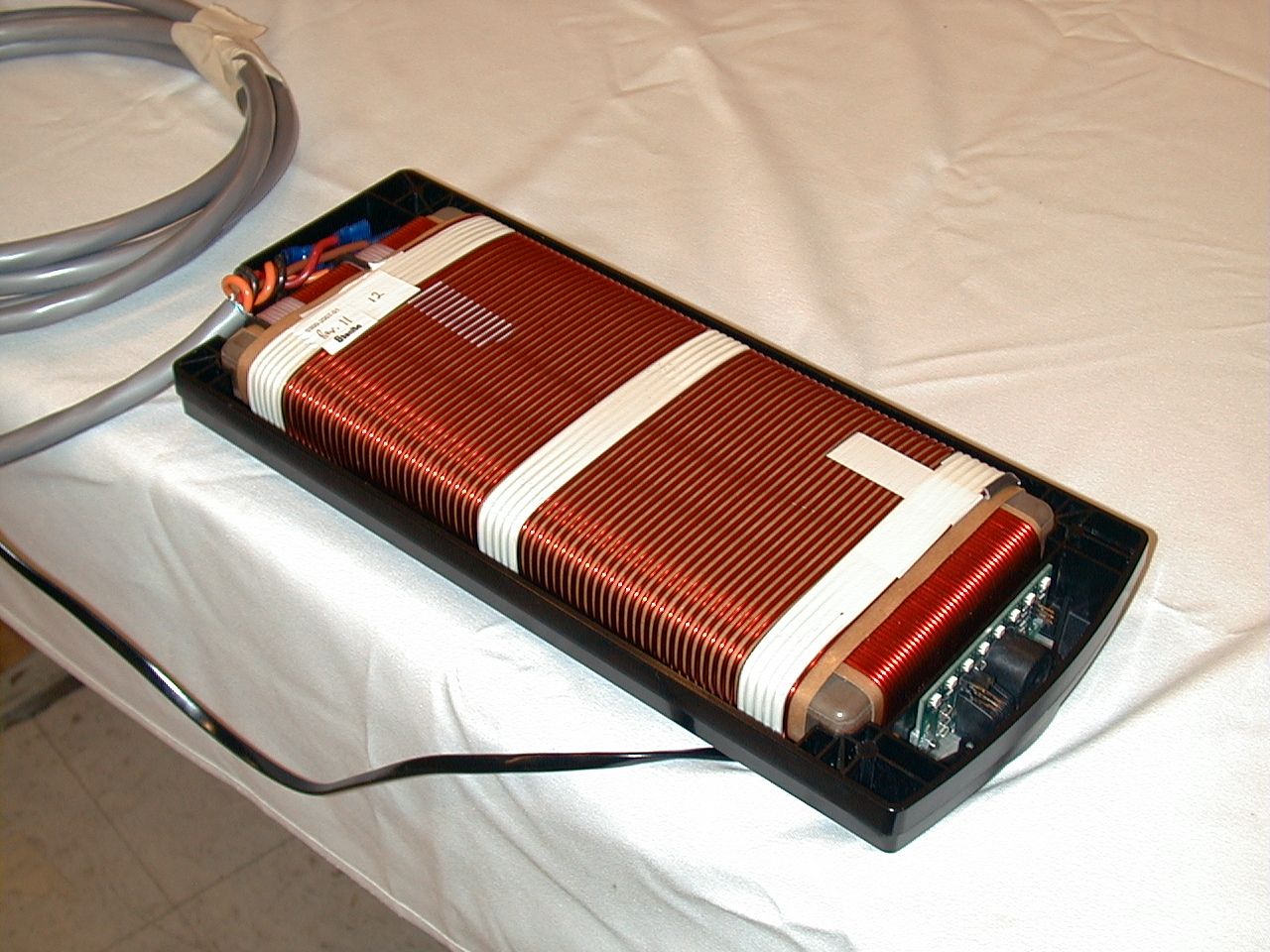
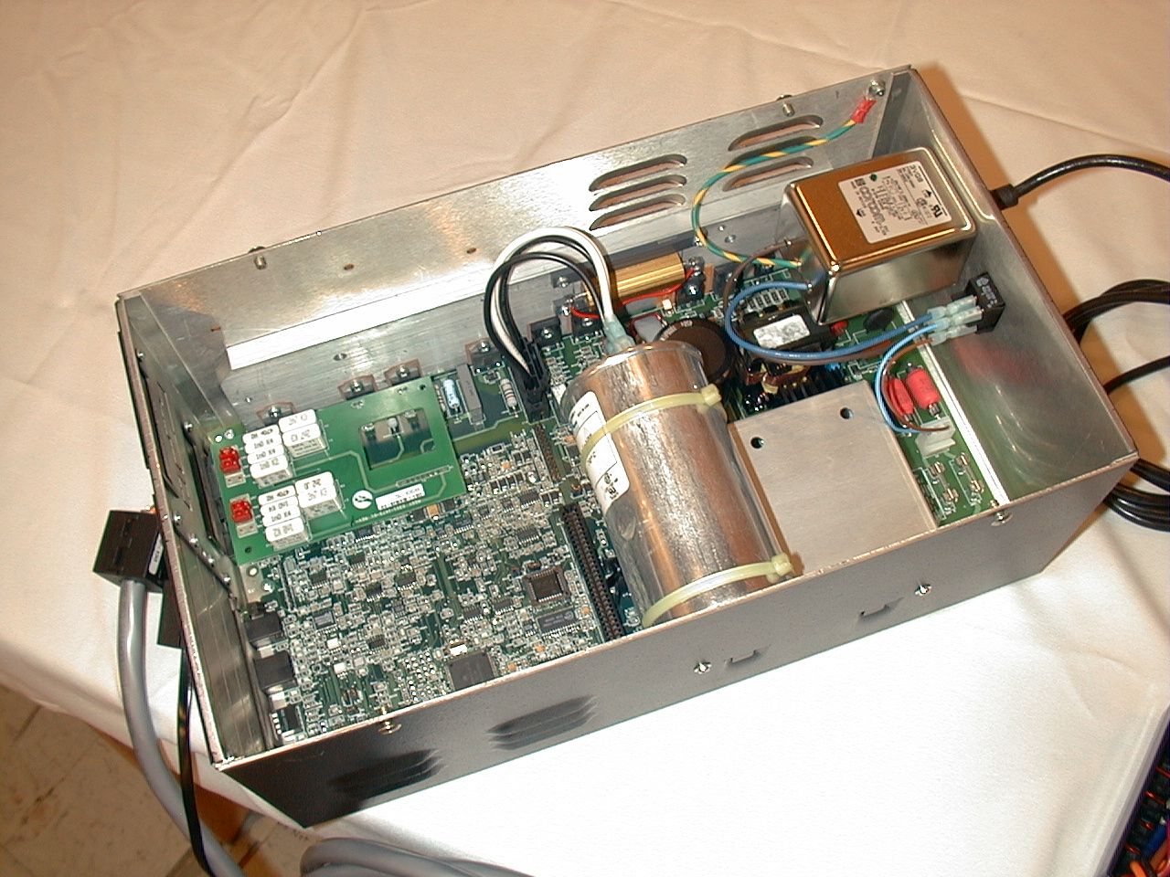
Planning Guide for Beta Test 8000-2599-01, Rev. A (10 pages)DEACTIVATION PRODUCTS1 Scan-Thru ™ Platform Proximity Deactivator ZBSTP-PK-1 Power Pack ZBSTP-PP Power Pad Antenna Contents About this Guide....................................................1 About the Deactivator............................................2 IMPORTANT SAFEGUARDS...............................5 Pre-Install Preparation ..........................................5 Specifications........................................................9 Declarations........................................................10 About this Guide This guide explains installation configurations, requirements, and specifications for the Scan-Thru Platform (STP) proximity deactivator. Other related documents are: • Installation Guide, 8000-2599-02 • Setup and Service Guide, 8000-2599-11 Note: The exact placement of the deactivator will depend on customer requirements. See your Sensormatic representative for this information. If you need assistance... Call Sensormatic Customer Support at: 1-800-543-9740 Scan-Thru, Sensormatic, and the Sensormatic logo are registered trademarks of Sensormatic Electronics Corporation. Other product names (if any) mentioned herein may be trademarks or registered trademarks of other companies. No part of this guide may be reproduced in any form without written permission from Sensormatic Electronics Corporation. © Copyright 1998. All rights reserved. MDR 12/98 2PLANNING GUIDE FOR BETA TEST STP POWER PAD DEACTIVATOR 8000-2599-01, Rev. A About the Deactivator The STP Deactivator (Figure 1) reliably deactivates Sensormatic UltraStrip II and Ultrastrip III security labels during the bar-code scanning process when: • Installed immediately downstream from the bar-code scanner. • UltraStrip II and III security labels are properly applied to items • Labeled items are moved properly across the antenna on their way to the bag well or bagging station. The deactivator consists of a hidden power pack, a countertop antenna with interconnect cable. • ZBSTP-PK-1 power pack controls antenna operation. At the rear of the pack is an ac receptacle for an 3m (10') power cord. In front is a power on LED; connections for the interconnect cable, an optional remote LED board or remote indicator module (see options), a laptop configurator, POS integration, and RS485 port; and DIP switches (SW1) for phase and sensitivity adjustments. A bracket enables the pack to attach to the underside of a countertop. • ZBSTP-PP Power Pad antenna generates a 15cm (6") (???-to be verified) high by 20cm (8") wide magnetic field above its surface to detect and deactivate UltraStrip II security labels. The antenna can be placed on the countertop, or using various brackets, mounted flush with the countertop, under the countertop, or when counter space is not available, over or on the side of the bagwell. The attached 2.5m (8') interconnect cable carries the label signal to the pack and the deactivate pulse to the antenna. CAUTION: The antenna cannot deactivate through metal. Do not place the antenna on, under, or near ferrous metal or cold-rolled steel. Optional status LEDs on the antenna indicate power on (green), security label deactivation (orange), and errors (red). An adjustable audio tone provides additional feedback that deactivation occurred. A second cable carries deactivator status signals to the LEDs in the antenna, or to a remote alarm, if used. Figure 1. STP deactivator Magnetic Media Safe Mode The magnetic field can be reduced before passing labeled magnetic media over the antenna, thus protecting the media from the deactivation field. This can be done manually using an optional footswitch. Status LEDs do not indicate when the field is reduced. Status LEDs Antenna Power Pack STP POWER PAD DEACTIVATOR 8000-2599-01, Rev. A PLANNING GUIDE FOR BETA TEST3 Options The following options can be ordered: ZBSTP-PK-B power pack mounting bracket (Figure 2) enables the power pack to attach to the underside of a countertop. Figure 2. Power pack mounting bracket ZBSTP-PP-IB indicator board (Figure 3) plugs into the bottom of the antenna to provide an audio/visual indication of operation. LEDs are visible through the top of the antenna. A cable connects the board to the power pack. Figure 3. Indicator board Remote Alarm Module (Figure 4) replaces the indicator board to position status LEDs closer to the operator. A cable connects the module to the power pack. Figure 4. Remote indicator module Antenna mounting brackets (Figure 5) are used to mount the antenna flush with the countertop, under the countertop, or when counter space is not available, over or on the side of the bagwell. These brackets are as follows: − ZBSTP-PP-B1 flush mount tray − ZBSTP-PP-B2 under counter bracket − ZBSTP-PP-B3 cantilever bracket (for bagwell) − ZBSTP-PP-B4 flip bracket (for bagwell) Note: Countertop mounting requires no additional bracketry. Figure 5. Antenna mounting brackets LWH Flush Mount Tray430mm201mm56mm Under Counter Brkt397mm226mm57mm Cantilever Bracket451mm236mm125mm Flip Down Bracket425mm195mm54mm Under Counter BracketFlush Mount Tray Flip Down Bracket Cantilever Bracket 4PLANNING GUIDE FOR BETA TEST STP POWER PAD DEACTIVATOR 8000-2599-01, Rev. A Component Description ZBSTPPK1 power pack (Figure 6). The pack contains the following components: a. AC input. Automatically adjusts for any input voltage from 100 to 250Vac and for 50/60Hz. b. On/Off switch. Turns power on and off. c. P16. Deactivation cable receptacle. d. P15. Indicator board receptacle. e. DS1. Power on indicator. f. P12. RS-232 software configurator port. g. P9. Scan Link I/O port. h. SW1. DIP switches for ac phase and gain adjustments. i. TB1. RS485 port. j. Antenna tuning jumpers. Inside the box. Figure 6. Power pack components Power Pad Antenna (Figure 7). Is a non- serviceable iron core assembly inside a plastic shell. The bottom of the antenna contains a well for the optional audio/visual indicator boar…
Text truncated - open the document above for the full version.
Block Diagram
Power Supply Line HVout Netural Line Sync HVena HVref1 HVref2 HV Control HVref1HVref HVref2 HVena HVenaHVena Charge Circuit HVin X Cap Y Cap ChgCtrl CapRef[1:2] Transmitter X Out Y Out TX Ctrl[1:6] Receiver Y In X In Rx Out[1:2] Rx Ctrl [1:4] Deactivation Circuit X Cap X Coil Y CapY Coil DXena DYena Cap Tuning X Out Y Out X In Y In System Controller Line Sync HV I/Ol [1:2]Chg I/O [1:3]DeacCtrl [1:2] TX Ctrl [1:6] I/O Bus [1:5] Rx I/O [1:6] Exp Bus 2nd Ant I/O RS-232 Remote Dip SW Scan Link RS-485 I/O Bus [1:6] Expansion 2nd Ant Bd Phase / Gain Select Configurator Indicator / Remote Control Center Scanner / POS RX1 5 Ohms CX1 100 uf L2 Y Coil L1 X Coil Scan-Thru Platform System Block Diagram Theory of Op.Dsn 12/08/98 Rev 1.0
Block Diagram
FCC ID: BVCDEACSTP I. General Information PRODUCT TESTED:Scan Thru Platform FCC ID: BVCDEACSTP TEST DATE:December 7-14, 1998 SUMMARY OF RESULTS: 47 CFR 15.207CONDUCTED EMISSIONSPASS 47 CFR 15.209RADIATED EMISSIONSPASS 1.1 Test Methodology Both conducted and radiated emissions testing were performed according to the procedures in ANSI C63.4-1992, and the requirements of 15.31, 15.33, 15.35, 15.207, and 15.209. Radiated emissions measurements were performed at a distance of 10 meters and the results extrapolated to the distance specified per 15.31 and 15.209. 1.2 Test Facility The shielded room conducted emissions measurement facility is located at Sensormatic Electronics Corporation Headquarters at 951 Yamato Road, Boca Raton, Florida, 33431. The radiated emissions site is located at Sensormatic Electronics Corporation manufacturing location, 6600 Congress Avenue, Boca Raton, Florida 33487. These sites have been found acceptable by and are on file with the FCC per FCC letter 31040/SIT 1300F2. 1.3 Test System Description. The Scan Thru Platform consists of a power pack and a separate antenna pad assembly connected by a 10′ cable. The power pack consists of a power supply, transmit electronics, receive electronics, deactivation electronics and scanner interface electronics. The power supply accepts inputs of 85 – FCC ID: BVCDEACSTP 250 V, 50-60 Hz. The antenna pad consists of 2 loop antennas that serve as transmit, receive and deactivation antennas on a multiplexed basis. The product tested was an engineering prototype built to production drawings. II. Conducted Emissions Conducted emissions data are presented in Section V “Data”, Part A “Conducted Emissions”. The product demonstrated compliance with the requirements of 15.207. Signals were sufficiently low to allow peak detector measurements to demonstrate compliance with the requirements. The product was tested at 120 V, 60 Hz. III. Radiated Emissions Radiated emissions data are presented in Section V “Data”, Part B “Conducted Emissions”. The product demonstrated compliance with the requirements of 15.209. Radiated emissions measurements were performed at 10 meters. Propagation loss was determined by square law extrapolation per 15.31(f)(2). Maximum radiation was determined by first assessing symmetry while applying incremental rotation of the measurement loop. The product exhibited quadrant symmetry. Measurements were taken at radials of 22.5° throughout one quadrant; the measurement antenna was rotated for maximum pickup about the vertical axis of the measurement antenna at each radial. The radiation pattern was also investigated with the measurement antenna in the horizontal plane. The maximum emission was determined to be with the measurement loop antenna in the vertical polarization, parallel to the long radiating loop of the pad. The product was tested at input voltages ranging from 102 – 138 V, 60 Hz with no measurable change in transmitter output. FCC ID: BVCDEACSTP IV.LIST OF MEASURING EQUIPMENT The equipment used for determining compliance of the Ultra Post system with the requirements of 15.207 and 15.209 is marked with an “X” in the first column of the table below. ModelDescriptionVendorSerial # X ALP -70Loop AntennaElectro Metrics 163 3110BBiconnical AntennaElectro Metrics 1017 3146Log Periodic AntennaEMCO 3909 3825/2Line Imp Stable NetworkEMCO 1562 X 3816/2NMLine Imp Stable NetworkEMCO 9703 1064 6060BFrequency GeneratorGiga-tronics 5850202 FM2000Isotropic Field MonitorAmplifier Research 15171 FP2000Isotropic Field ProbeAmplifier Research 15214 888LevelerAmplifier Research 14998 75A220Low Band AmplifierAmplifier Research 15208 10W1000AHigh Band AmplifierAmplifier Research 15138 PEFT JuniorEFT GeneratorHaefely Trench 083 180-16 PEFT JuniorCapacitive Cable ClampHaefely Trench 083-078-31 NSG435ESD SimulatorSchaffner 1197 NSG431ESD SimulatorSchaffner 1267 X HP8591EMEMC AnalyzerHewlett - Packard 3520A00190 Power SourcePacific Instruments F-2031EM Injection ClampFischer Cust. Comm. 30 FCC-801-M3-16Coupling Decoupling NwkFischer Cust. Comm. 58 FCC-801-M3-16Coupling Decoupling NwkFischer Cust. Comm. 59 F-33-1RF Current Probe Fischer Cust. Comm. 304 EM 7600Transient LimiterElectro-Metrics 187 Roberts AntTunable Dipole SetCompliance Design 003282 Roberts AntTunable Dipole SetCompliance Design 003283 HP8594ESpectrum AnalyzerHewlett Packard 3246A00300 X HP8447F Opt 64Dual PreamplifierHewlett Packard 2805A03473 FCC ID: BVCDEACSTP V.Data Part A contains conducted emissions data; Part B contains radiated emissions data. Part A Conducted Emissions Project Name ScanThru Platform Filename STP_Conducted Emissions, FCC EUT Name STP Serial Number Engineer Steve Maitin Phone Number Date of Test 12/14/98 1:33:05 PM Test Name Conducted Emissions 47CFR15.207 Reg. Technician Steve Krizmanich Proj. Ldr Don Umbdenstock Comments Table 1, Signal List SignalFreq (MHz) Peak Amp (dBuV) QP Amp (dBuV) Avg Amp (dBuV) Corrections (dB) Limit (dB) 125.35275538.7425.383.100.0048 223.59969531.2723.5611.030.0048 31.68281333.8630.8915.910.0048 FCC ID: BVCDEACSTP Figure 1. Line 1 Conducted Emissions FCC ID: BVCDEACSTP Figure 2. Line 2 Conducted Emissions. FCC ID: BVCDEACSTP Part BRadiated Emissions Project Name ScanThru Platform Filename Scan Thru Platform Radiated Emissions EUT Name STP Serial Number Engineer Steve Maitin Phone Number Date of Test 12/10/98 Test Name Radiated Emissions 47CFR15.209 Reg. Technician Steve Krizmanich Proj. Ldr Don Umbdenstock FreqS.A.Ant Fact DCFActualLimitDetBW Comments kHzdBdBuV/mdBdBuV/mdBuV/mkHz 5824.6 62.5 -59.128 32.3/300peak9 5824.6 62.5 -59.128 32.3/300peak1Note 3. 116-8 56.5 -59.1-10.6 26.3/300peak1system noise floor 1742.7 53 -59.1-3.4 22.8/300peak1 232-13 50 -59.1-22.1 20.3/300peak1noise floor 290-3 48.3 -59.1-13.8 18.4/300peak1 348-14 47 -59.1-26.1 16.8/300peak1noise floor 406-11 46 -59.1-24.1 15.4/300peak1ambient 464-17 44.9 -59.1-31.2 14.3/300peak1noise floor 522-17 43.9 -19.17.8 33.3/30peak1noise floor 580-14 43.2 -19.110.1 …
Text truncated - open the document above for the full version.
ID Label/Location Info
THIS DRAWING MAY CONTAIN PATENTED OR PROPRIETARY INFORMATION AND MUST NOT BE USED FOR MANUFACTUR- ING OR ANY PURPOSE DETRI- MENTAL TO SENSORMATIC ELECTRONICS. ACCEPTANCE OF THIS DRAWING WILL BE CONSTRUED AS AN AGREE- MENT TO AND ACCEPTANCE OF THE FOREGOING. DECIMALS X.X = +/- .5mm X.XX = +/- .3mm X.XXX = +/- .1mm FINISH N/A ANGLES +/- 1/2 DEGREE RELEASE APP’D CHECKED DRAWN R. CERASINI APPROVALS DIMENSIONS ARE SHOWN IN MILLIMETERS DATE 5-23-94 SENSORMATIC ELECTRONICS CORP. DEERFIELD BEACH, FLORIDA SIZE A DRAWING NUMBER 2402-0469-00 TITLE LABEL,UNIVERSAL REV BE SHEET 2 OF 49 ENGR TOLERANCES ARE: MATERIAL 1 Sensormatic THE WORLD LEADER IN LOSS PREVENTION TECHNOLOGY 1.54 MIN 4 x V ~ VOLTAGE SYMBOL PRINT SYMBOL AS SHOWN NOTES: 1 MATERIAL: MAKE FROM 2402-0357-08. 2. FIELD VARIABLES ARE SHOWN AS HEXAGONS. SEE ATTACHED LISTING FOR DESCRIPTIONS. 12 1 2 3 4 5 67 13 8 11 10 9 PART NO.NO.DESCRIPTION 2402-0469-45PRINT THE FOLLOWING FIELD INFORMATION PRODUCT CODES1 REG ID2REG ID: DEAC STP-PP PART NUMBER3P/N: 0309-0068-01 REV (CURRENT) SERIAL NUMBER4S/N: (CURRENT) RATING5 100-240V~ 2A 50-60Hz UL LOGO6( PRINT WHERE SHOWN, ON PAGE 3 FIG. C ) C-UL LOGO7( PRINT cUL SYMBOL WITHOUT TEXT, AS ON PAGE 3, FIG. F) COUNTRY OF MANUFACTURE8MADE IN (COUNTRY OF ORIGIN) (FOR COUNTRY OF ORIGIN PRODUCTION CONTROL TO INSERT COUNTRY BASED UPON MANUFACTURING LOCATION) 9 FCC10FCC ID: BVCDEACSTP THIS DEVICE COMPLIES WITH PART 15 OF THE FCC RULES. OPERATION IS SUBJECT TO THE FOLLOWING TWO CONDITIONS: (1) THIS DEVICE MAY NOT CAUSE HARMFUL INTERFERENCE, AND (2) THIS DEVICE MUST ACCEPT ANY INTER- FERENCE RECEIVED, INCLUDING INTERFERENCE THAT MAY CAUSE UNDESIRED OPERATION. MFG BARCODE11(LOCATE AS SHOWN) S.E.C. LOGO12(LOCATE AS SHOWN) CE13(PRINT WHERE SHOWN, VERTICAL DIMENSION AT LEAST 5 mm) NOTES/COMMENTSVARIABLES ARE DEFINED IN THE “DESCRIPTION” COLUMN. ITEMS LISTED IN PARENTHESIS ARE NOT VARIABLES, BUT DEFINE THE VARIABLE FOR THE RESPECTIVE LINE ITEM. LABEL PART NO. 2402-0469-45REVBB
ID Label/Location Info
Scan Thru Platform, Bottom View – Compliance Label, containing FCC label requirements.
Operational Description
Scan Thru Platform Theory of Operation Preliminary 12/09/98 Overview - The ScanThru Platform (STP) utilizes Label detection to trigger the Deactivation sequence with the power supply and interface circuits supporting these two main functions. The STP consists of a separate power pack and antenna assemblies. Figure 1 shows a block diagram of this system. The Power pack consists of one large circuit board and a capacitor tuning board. The antenna consists of two windings which are used for transmit, receive and deactivation. The system board can be divided into several sections; power supply, controller, transmitter, receiver, high voltage control, charge, deactivation and interface sections. The following describes each of these sections in more detail: Power Supply Line HV out Net ural Line Syn c HV ena HV r ef 1 HV ref 2 HV C o nt r o l HV ref 1HV ref HV ref 2 HV e n a HV enaHV ena Charge Circuit HV in X Cap Y Cap ChgCt rl CapRef[1:2] Transmitter X Out Y Out TX Ctrl[1:6] Receiver Y In X In Rx O u t [ 1 : 2 ] Rx Ctrl [1:4] Deactivation Circuit X Cap X Coil Y CapY Coil DXena DY ena Cap Tuning X Out Y Out X In Y In System Controller Line Sy n c HV I/Ol [1:2]Chg I/O [1:3]DeacCtr l [1:2] T X C t rl [ 1:6 ] I/O Bu s [ 1:5] R x I/ O [1 :6] Ex p B u s 2nd A nt I/O RS-232 Remote Dip SW Scan Lin k RS-485 I/O Bu s [ 1:6] Expans ion 2nd A nt Bd Phase / Gain Select Configurator Indic ator / Remot e Cont rol Center Scanner / POS RX1 5 Ohms CX1 100 uf L2 Y Coil L1 X Coil Scan-Thru Platform System Block Diagram Theory of Op.Dsn 12/08/98 Rev 1.0 1. Power Supply – The purpose of the power supply is to generate the low voltage bias supplies required by the internal circuitry and to generate the high voltage needed for deactivation as well as to provide a zero crossing output to the microprocessor. The power supply actually consist of two separate switch mode power supplies; one for the bias and one for the high voltage. Both supplies are connected off line and utilize output transformers to achieve isolation. The bias supply is a standard fly-back converter operating at 37Khz. This supply has three outputs; 25 Vdc, +12 Vdc and –12 Vdc. Post regulation utilizing a three terminal regulator is used to generate the +5 Vdc logic supply from the +12V output. The high voltage supply is also a fly-back converter that has been modified to achieve good power factor correction utilizing a simple on-off control method. The zero crossing circuit provides a 30us pulse at the rising edge of the zero crossing of the AC mains. This signal is used to provide synchronization of the Ultra*Max transmit and receive functions. 2. Controller – The purpose of the controller section is to monitor and control all system operation. The control section consists of a microprocessor, memory, a CPLD (Complex Programmable Logic Device) and associated logic used to “glue” these functions together. The microprocessor, a Motorola 68HC12 device contains internal memory, timers and analog to digital converters. A flash EEProm is used to store the program executable code and static ram is used for buffers and variable storage. The CPLD is used to generate the various system clocks and to multiplex the microprocessor timer outputs to each of the other sections. The microprocessor controls virtually all of the critical system functions including HV set point control, Charge and Deactivation switch timing, Transmitter power and timing and receiver operation. 3. Transmitter - The purpose of the transmitter is to generate the transmit field used to excite the Ultra*Max label. The timing and amplitude of the trasmitter is controlled by the microprocessor. A separate 116khz signal is used by this section to generate the 58khz transmit frequency. There are separate outputs for the x and the y antenna windings. A standard half bridge driver is used to drive the MosFet output drivers. The output of each transmitter is series resonated at 58khz using capacitors on the Cap tuning board which are matched to the inductance of each output winding. These capacitors also are used to achieve isolation between the high voltage output and the low voltage transmitter circuits. 4. Receiver - The purpose of the receiver is to detect the presence of the Ultra*Max label. The input of the receiver is capacity coupled to the transmitter output. The receiver consists of a RF front end section and a base band output section. The input section consists of an input muxiplexer, low noise amplifiers, blanking components, a programmable gain stage, a band pass filter stage which feeds an synchronous demodulator or mixer. The function of the front end is to amplify and filter the very small tag signal. This signal 58khz label signal is mixed with a 58khz carrier. The output frequency of the mixer consists of the sum and differences of the label frequency and the carrier frequency. If the label is at exactly 58khz the output of the mixer will be DC and 116khz. The amplitude is a function if the label amplitude and the phase difference between the label signal and the carrier signal. Because the phase relationship between the label and carrier is dependent upon label position and orientation to the receive antenna, two separate mixers are used with the separate carriers which are phased 90° apart. The output of each mixer is then low passed filtered at approximately 500 Hz to eliminate the high frequency products and to provide rejection of out of band noise. This signal is then full wave rectified to achieve compatibility with the microprocessor single ended A/D converter. 5. HV Control – The purpose of the high voltage control circuit is to provide set point and over voltage protection functions for the high voltage power supply. The inputs to this circuit consist of an enable signal from the microprocessor and two reference feedback signals from the high voltage output. One reference signal is utilized as an over voltage shutdown while the second reference is used for set poin…
Text truncated - open the document above for the full version.
Schematics
FCC ID: BVCDEACSTP I. General Information PRODUCT TESTED:Scan Thru Platform FCC ID: BVCDEACSTP TEST DATE:December 7-14, 1998 SUMMARY OF RESULTS: 47 CFR 15.207CONDUCTED EMISSIONSPASS 47 CFR 15.209RADIATED EMISSIONSPASS 1.1 Test Methodology Both conducted and radiated emissions testing were performed according to the procedures in ANSI C63.4-1992, and the requirements of 15.31, 15.33, 15.35, 15.207, and 15.209. Radiated emissions measurements were performed at a distance of 10 meters and the results extrapolated to the distance specified per 15.31 and 15.209. 1.2 Test Facility The shielded room conducted emissions measurement facility is located at Sensormatic Electronics Corporation Headquarters at 951 Yamato Road, Boca Raton, Florida, 33431. The radiated emissions site is located at Sensormatic Electronics Corporation manufacturing location, 6600 Congress Avenue, Boca Raton, Florida 33487. These sites have been found acceptable by and are on file with the FCC per FCC letter 31040/SIT 1300F2. 1.3 Test System Description. The Scan Thru Platform consists of a power pack and a separate antenna pad assembly connected by a 10′ cable. The power pack consists of a power supply, transmit electronics, receive electronics, deactivation electronics and scanner interface electronics. The power supply accepts inputs of 85 – FCC ID: BVCDEACSTP 250 V, 50-60 Hz. The antenna pad consists of 2 loop antennas that serve as transmit, receive and deactivation antennas on a multiplexed basis. The product tested was an engineering prototype built to production drawings. II. Conducted Emissions Conducted emissions data are presented in Section V “Data”, Part A “Conducted Emissions”. The product demonstrated compliance with the requirements of 15.207. Signals were sufficiently low to allow peak detector measurements to demonstrate compliance with the requirements. The product was tested at 120 V, 60 Hz. III. Radiated Emissions Radiated emissions data are presented in Section V “Data”, Part B “Conducted Emissions”. The product demonstrated compliance with the requirements of 15.209. Radiated emissions measurements were performed at 10 meters. Propagation loss was determined by square law extrapolation per 15.31(f)(2). Maximum radiation was determined by first assessing symmetry while applying incremental rotation of the measurement loop. The product exhibited quadrant symmetry. Measurements were taken at radials of 22.5° throughout one quadrant; the measurement antenna was rotated for maximum pickup about the vertical axis of the measurement antenna at each radial. The radiation pattern was also investigated with the measurement antenna in the horizontal plane. The maximum emission was determined to be with the measurement loop antenna in the vertical polarization, parallel to the long radiating loop of the pad. The product was tested at input voltages ranging from 102 – 138 V, 60 Hz with no measurable change in transmitter output. FCC ID: BVCDEACSTP IV.LIST OF MEASURING EQUIPMENT The equipment used for determining compliance of the Ultra Post system with the requirements of 15.207 and 15.209 is marked with an “X” in the first column of the table below. ModelDescriptionVendorSerial # X ALP -70Loop AntennaElectro Metrics 163 3110BBiconnical AntennaElectro Metrics 1017 3146Log Periodic AntennaEMCO 3909 3825/2Line Imp Stable NetworkEMCO 1562 X 3816/2NMLine Imp Stable NetworkEMCO 9703 1064 6060BFrequency GeneratorGiga-tronics 5850202 FM2000Isotropic Field MonitorAmplifier Research 15171 FP2000Isotropic Field ProbeAmplifier Research 15214 888LevelerAmplifier Research 14998 75A220Low Band AmplifierAmplifier Research 15208 10W1000AHigh Band AmplifierAmplifier Research 15138 PEFT JuniorEFT GeneratorHaefely Trench 083 180-16 PEFT JuniorCapacitive Cable ClampHaefely Trench 083-078-31 NSG435ESD SimulatorSchaffner 1197 NSG431ESD SimulatorSchaffner 1267 X HP8591EMEMC AnalyzerHewlett - Packard 3520A00190 Power SourcePacific Instruments F-2031EM Injection ClampFischer Cust. Comm. 30 FCC-801-M3-16Coupling Decoupling NwkFischer Cust. Comm. 58 FCC-801-M3-16Coupling Decoupling NwkFischer Cust. Comm. 59 F-33-1RF Current Probe Fischer Cust. Comm. 304 EM 7600Transient LimiterElectro-Metrics 187 Roberts AntTunable Dipole SetCompliance Design 003282 Roberts AntTunable Dipole SetCompliance Design 003283 HP8594ESpectrum AnalyzerHewlett Packard 3246A00300 X HP8447F Opt 64Dual PreamplifierHewlett Packard 2805A03473 FCC ID: BVCDEACSTP V.Data Part A contains conducted emissions data; Part B contains radiated emissions data. Part A Conducted Emissions Project Name ScanThru Platform Filename STP_Conducted Emissions, FCC EUT Name STP Serial Number Engineer Steve Maitin Phone Number Date of Test 12/14/98 1:33:05 PM Test Name Conducted Emissions 47CFR15.207 Reg. Technician Steve Krizmanich Proj. Ldr Don Umbdenstock Comments Table 1, Signal List SignalFreq (MHz) Peak Amp (dBuV) QP Amp (dBuV) Avg Amp (dBuV) Corrections (dB) Limit (dB) 125.35275538.7425.383.100.0048 223.59969531.2723.5611.030.0048 31.68281333.8630.8915.910.0048 FCC ID: BVCDEACSTP Figure 1. Line 1 Conducted Emissions FCC ID: BVCDEACSTP Figure 2. Line 2 Conducted Emissions. FCC ID: BVCDEACSTP Part BRadiated Emissions Project Name ScanThru Platform Filename Scan Thru Platform Radiated Emissions EUT Name STP Serial Number Engineer Steve Maitin Phone Number Date of Test 12/10/98 Test Name Radiated Emissions 47CFR15.209 Reg. Technician Steve Krizmanich Proj. Ldr Don Umbdenstock FreqS.A.Ant Fact DCFActualLimitDetBW Comments kHzdBdBuV/mdBdBuV/mdBuV/mkHz 5824.6 62.5 -59.128 32.3/300peak9 5824.6 62.5 -59.128 32.3/300peak1Note 3. 116-8 56.5 -59.1-10.6 26.3/300peak1system noise floor 1742.7 53 -59.1-3.4 22.8/300peak1 232-13 50 -59.1-22.1 20.3/300peak1noise floor 290-3 48.3 -59.1-13.8 18.4/300peak1 348-14 47 -59.1-26.1 16.8/300peak1noise floor 406-11 46 -59.1-24.1 15.4/300peak1ambient 464-17 44.9 -59.1-31.2 14.3/300peak1noise floor 522-17 43.9 -19.17.8 33.3/30peak1noise floor 580-14 43.2 -19.110.1 …
Text truncated - open the document above for the full version.
Test Report
FCC ID: BVCDEACSTP I. General Information PRODUCT TESTED:Scan Thru Platform FCC ID: BVCDEACSTP TEST DATE:December 7-14, 1998 SUMMARY OF RESULTS: 47 CFR 15.207CONDUCTED EMISSIONSPASS 47 CFR 15.209RADIATED EMISSIONSPASS 1.1 Test Methodology Both conducted and radiated emissions testing were performed according to the procedures in ANSI C63.4-1992, and the requirements of 15.31, 15.33, 15.35, 15.207, and 15.209. Radiated emissions measurements were performed at a distance of 10 meters and the results extrapolated to the distance specified per 15.31 and 15.209. 1.2 Test Facility The shielded room conducted emissions measurement facility is located at Sensormatic Electronics Corporation Headquarters at 951 Yamato Road, Boca Raton, Florida, 33431. The radiated emissions site is located at Sensormatic Electronics Corporation manufacturing location, 6600 Congress Avenue, Boca Raton, Florida 33487. These sites have been found acceptable by and are on file with the FCC per FCC letter 31040/SIT 1300F2. 1.3 Test System Description. The Scan Thru Platform consists of a power pack and a separate antenna pad assembly connected by a 10′ cable. The power pack consists of a power supply, transmit electronics, receive electronics, deactivation electronics and scanner interface electronics. The power supply accepts inputs of 85 – FCC ID: BVCDEACSTP 250 V, 50-60 Hz. The antenna pad consists of 2 loop antennas that serve as transmit, receive and deactivation antennas on a multiplexed basis. The product tested was an engineering prototype built to production drawings. II. Conducted Emissions Conducted emissions data are presented in Section V “Data”, Part A “Conducted Emissions”. The product demonstrated compliance with the requirements of 15.207. Signals were sufficiently low to allow peak detector measurements to demonstrate compliance with the requirements. The product was tested at 120 V, 60 Hz. III. Radiated Emissions Radiated emissions data are presented in Section V “Data”, Part B “Conducted Emissions”. The product demonstrated compliance with the requirements of 15.209. Radiated emissions measurements were performed at 10 meters. Propagation loss was determined by square law extrapolation per 15.31(f)(2). Maximum radiation was determined by first assessing symmetry while applying incremental rotation of the measurement loop. The product exhibited quadrant symmetry. Measurements were taken at radials of 22.5° throughout one quadrant; the measurement antenna was rotated for maximum pickup about the vertical axis of the measurement antenna at each radial. The radiation pattern was also investigated with the measurement antenna in the horizontal plane. The maximum emission was determined to be with the measurement loop antenna in the vertical polarization, parallel to the long radiating loop of the pad. The product was tested at input voltages ranging from 102 – 138 V, 60 Hz with no measurable change in transmitter output. FCC ID: BVCDEACSTP IV.LIST OF MEASURING EQUIPMENT The equipment used for determining compliance of the Ultra Post system with the requirements of 15.207 and 15.209 is marked with an “X” in the first column of the table below. ModelDescriptionVendo…
Text truncated - open the document above for the full version.
Contact Information
Applicant
Mark D. Alexis(Manager Regulatory Compliance)
Technical Contact
Sensormatic Electronics CorporationDonald J Umbdenstock
[email protected]561 989 7454
951 Yamato Road · Boca Raton, Florida · United States
Technical Specifications
| # | Rule Parts | Frequency Range | Power Output |
|---|---|---|---|
| 1 | 15.209 | 0.058 MHz - 0.058 MHz | - |
Other Applications from Tyco Safety Products/Sensormatic
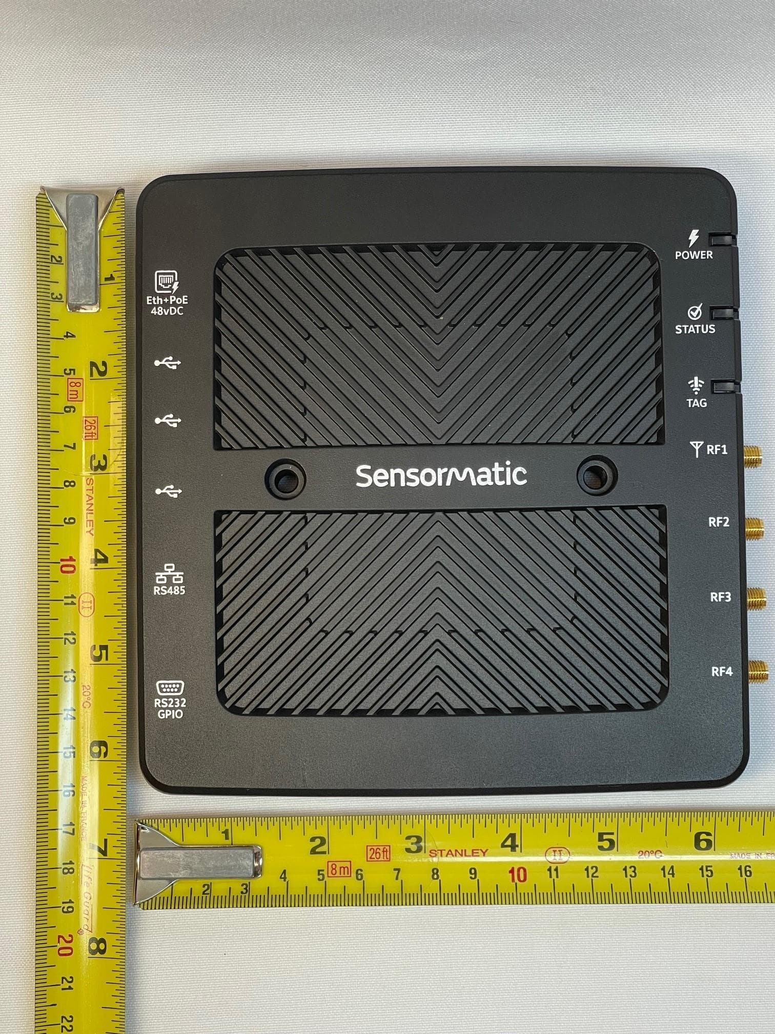
BVCIDX5000
Jun 23, 2026UHF RFID Reader
Equipment Class
DSS - Part 15 Spread Spectrum TransmitterBVCAMS1137H
Dec 22, 2025Anti Theft System - Electronic Asset Security
Equipment Class
FAP - Part 15 Anti-Pilferage DeviceBVCAMB9012
Sep 10, 2024Label Deactivator Controller
Equipment Class
DCD - Part 15 Low Power Transmitter Below 1705 kHz
BVC-4000-PI26
Sep 24, 2015RM2L-4000-P126, RM2-4000-P126
Equipment Class
DXX - Part 15 Low Power Communication Device Transmitter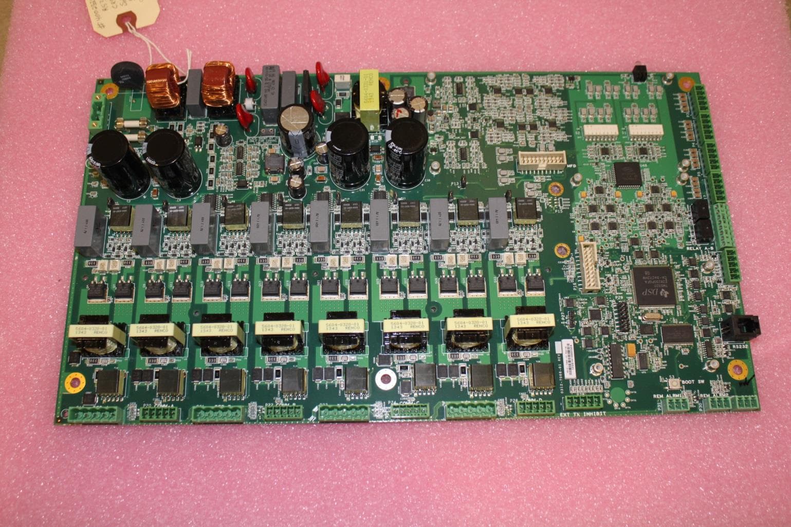
BVCAMS90604
May 20, 2014Anti-pilferage Device
Equipment Class
FAP - Part 15 Anti-Pilferage Device