CFSK3852Cellular Control Channel Transceiver
Ademco Inc.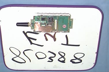
Click to zoom
Application Details
- Equipment Class
- TNB - Licensed Non-Broadcast Station Transmitter
- Date of Grant
- Aug 26, 1999
- Application Purpose
- Original Equipment
- Date of Application
- May 27, 1999
- Equipment Note
- Cellular Control Channel Transceiver
- Frequency Range
- 824.04000000 - 848.94000000
- Company
- Ademco Inc.
- Country
- United States
Documents & Files
Document Text
Text extracted from the exhibit documents filed with the FCC. Open a document above to read the original.
Users Manual
K3852K3852 CellularCellular Control Channel TransceiverControl Channel Transceiver Installation and Setup GuideInstallation and Setup Guide NOW PRO* ENABLED! *PROGRAMMERLESS REGISTRATION OPTION K3852V1 2/99 – 2 – Table of Contents List of Terms...................................................................................................................................................2 Section 1. General Information.......................................................................................................................3 Introduction.......................................................................................................................................3 System Features................................................................................................................................3 Section 2. Quick Start/Programming Guide....................................................................................................4 Section 3. Installation and Setup.....................................................................................................................6 Removing the Lower Cover..............................................................................................................6 Initial Power-Up Sequence...............................................................................................................7 Selecting a Radio Installation Site....................................................................................................8 Testing the Installation......................................................................................................................9 Section 4. Programming the K3852..............................................................................................................10 Using a 7720P Programming Tool..................................................................................................10 Subscriber Information....................................................................................................................11 Pulse/Delay Zone Selection............................................................................................................12 Inverted Zone Selection..................................................................................................................13 Restoral Reporting Zone Selection.................................................................................................14 Open/Close, Telco, Tamper Zone Selection...................................................................................15 System Options...............................................................................................................................15 Redundant Central Station Reporting.............................................................................................16 Exiting Program Mode, Setting Defaults and Assigning Passwords...............................................17 Section 5. Registration..................................................................................................................................18 Section 6. Mounting and Wiring...................................................................................................................21 Section 7. Operation Overview.....................................................................................................................26 Section 8. Keyboard Commands...................................................................................................................28 Section 9. Troubleshooting............................................................................................................................30 UL Requirements..........................................................................................................................................32 Specifications................................................................................................................................................34 Summary of Connections Diagram...............................................................................................................35 List of Terms AMPS:Acronym for Advanced Mobile Phone System, which is the existing analog mobile phone system used for cellular communication in North America. A Side / B-Side:The FCC has divided the spectrum allocated to cellular communication between two carriers in each geographic location: A and B. The “B” side is operated by the local telephone company (known as wireline), while the “A” side is run by a competitor (known as non-wireline). Cell: The equipment, including antennas, RF transmitters, RF receivers, that is used to establish and route communications between a mobile cellular radio and its intended end point. Control Channel:Any one of several dedicated RF channels that are used by a cellular radio to register its MIN with a local cell and to periodically check in with that cell. The control channel is also used by the radio to “dial” a phone number through the cell. Additionally, control channels are used by the cell to “ring” a mobile cellular radio. MIN: Acronym for Mobile Identification Number, which is a cellular radio’s unique, 10-digit “phone number.” SS7: Acronym for Signaling System Seven, which is the network that is used by all telephone companies for dialing and establishing all cellular and land-line phone calls. Voice Channel:Any one of many dedicated RF channels used for transmitting and receiving audio data between a mobile phone and a cell. (Not used with the K3852.) – 3 – Section 1: General Information Introduction The K3852 is the subscriber end of the AlarmNet C reporting system. It is comparable to a digital communicator, but instead of transmitting signals over the telephone lines, it transmits radio signals to the central monitoring station using the control channel of the AMPS cellular phone n…
Text truncated - open the document above for the full version.
Operational Description
K3852(NSA1000)ADEMCO Group, Niigata Seimitsu Co., Ltd. Page 1/6 K3852(NSA1000) System Description (refer to the block diagram) 1.1 Receiver (RX) section 1.1.1 Input ( receiving frequency) fri=869.040 to 893.970 MHz, 30KHz step 1.1.2 Description The RX signal caught by Helical antenna is fed to RX RF amplifier and mixer (Q101,Q121) through the duplexer (F100) with band-pass filtering. ‡ See characteristics of the duplexer (DFYGR836CR881NHA). Then the RX signal amplified by Q101 and applied to RX mixer1, Q121 (RX MIX1) through the SAW band-pass filter (F102) which reduces out of band noises and spurious. ‡ See characteristics of the SAW band-pass filter. The signal of input is mixed with the local frequency (fo1) which is generated by the VCO (X911) that works as a frequency synthesizer combined with phase locked loop IC, U900, at the first mixer Q121. The output of the first mixer generates first IF frequency (fi1) , 86.460MHz and this signal is delivered to the first IF filter (F102). The fi1 and fo1 is calculated as below; The second IF frequency fi2=60KHz The second local frequency fo2= 14.4MHz(TCXO frequency) x6 =86.400MHz Therefore, fi1= fi2 + fo2 =86.460 MHz Therefore, fo2=fri + fi1 =955.500 to 980.430MHz, 30KHz step The F102 is a SAW filter with 86.460MHz of center frequency that has very good shape factor. This filter works to eliminate alternate frequency (fi1+/- 60KHz) and image frequency of second mixer (fi1+120KHz=86.58MHz) that rejection ratio should satisfy the specification. ‡ See characteristics of the SAW IF filter. The fi1 signal is amplified by Q131 in order to obtain enough gain of RX section. The IC, U101, is incorporating the following function; Second Mixer with image frequency cancellation circuit, Band-pass filter with 60KHz of center frequency Second IF amplifier FM detector RSSI (Receiving Signal Strength Indicator) output) ‡ See block diagram and characteristics of TA31181FN. The second local frequency (fo2=86.460MHz) is obtained to be multiplied by six(6) of TCXO frequency (f TCXO=14.4000MHz). The f TCXO is fed to tuned amplifier inside of U900 and Q171. The about 86 MHz tuning circuit, L171, L172, C174 and C175, picks up the 86.400MHz which is a six times harmonics of f TCXO. The second mixer inside of U101 generates a second IF signal which frequency is K3852(NSA1000)ADEMCO Group, Niigata Seimitsu Co., Ltd. Page 2/6 60KHz The fo2 is split into 2 path inside of U101, one for in-phase signal and other for quadrature signal. These signals are applied to two second mixers. The output of second mixers is synthesized with 90 degrees phase shifting for quadrature mixer side. This function works to make cancellation of the image frequency, about 30dB rejection ratio. About 75 dB total image rejection ratio for fi2 can be obtained to combine with F102, even though such lower IF frequency. The sharp narrow (+/-15KHz) BPF having 60KHz-center frequency inside U101 works to eliminate adjacent channel. The center frequency of 60KHz BPF is synchronizing to its clock frequency, 14.400MHz that is fed from TCXO. So very stable filter characteristics can be obtained due to very stable frequency of TCXO. After 60KHz filtering, the signal is amplified and limiting its amplitude by limiter. Then quadrature detector that is incorporated into U101 demodulates the FM signal. The center frequency is also synchronizing to 14.4 MHz like 60KHz filter. RSSI (DC level) is obtained to gather second IF signal. 1.2 Transmitting (TX) section 1.2.1 TX frequency ftx= 824.040 to 848.940MHz, 30KHz step 1.2.2 Activation control for the transmitter When TX starts to activate, TX VCO and TX section of the U101 simultaneously. The TX VCO is switched by Q701 that is controlled by CPU with active high level, and TX section synthesizer of U101 can be controlled by data from CPU through its serial data transmission line, SYE, SYD and SYC. After a few milliseconds waiting, the TX switch, Q606 and Q607 work to turn on. Then all TX sections as U201 (buffer amplifier), Q603 (TX driver), Q604 ( TX final power amplifier), U241(APC circuit) Q607 and Q606 (power switch) become to activate. Note that TX switch circuit, Q606 and Q607 are not switched on if TX synthesizer circuit including VCO has already activating. The synthesizer must be priority in order to activate all TX circuits. The emitter of Q607 detects whether synthesizer is activating, i.e., Q607 must be low level for activation. Usually it is switched on, then, enough current capacity is applied to final stage of TX power amplifier VCC(6.0V). 1.2.3 TX VCO and Modulator The basic TX VCO circuit is built of X931. It is controlled by applied DC voltage that is the output of the synthesizer, U900, through low pass filter, C939, C935, R932, R933 and C933. The controlled voltage is within 0.8 to 2.2V to cover the TX frequency range. The CPU is monitoring synthesizer lock-upped DC voltage through the TVL line. If this voltage is out of 0.8 to 1.0 volt at minimum frequency, CH0991, the DC K3852(NSA1000)ADEMCO Group, Niigata Seimitsu Co., Ltd. Page 3/6 voltage to TX V.C.O applied from CPU through TVA line is adjusted until becoming specified range since this loop works as negative feedback circuitry. After fixing DC voltage at CH0991, the synthesizer frequency moves to upper frequency, CH0799 and monitored this frequency by CPU through TLV line. If this DC voltage is lower than 2.2volt, this VCO is accepted, otherwise, higher than 2.2V, this is failure VCO and rejected. At the same time, lock condition is monitored by CPU and unconditionally is rejected if unlocked condition occurs. TX V.C.O is also used for the modulator. The modulation signal comes from the base band processor through MOD line. R401 and R934 to be obtained optimized modulation level divide this signal. ‡ Refer to paragraph of Modulation 1.2.4 TX power stage The fig.1.2.4.1 shows block diagram of TX power stage for K3852(NSA1000). The modulated FM signal generated by TX VCO is amplified by U2…
Text truncated - open the document above for the full version.
Parts List/Tune Up Info
Parts List For Main PCB 1/6 CC040C101CAPACITOR CC220C102CAPACITOR CC101C103CAPACITOR CC020C104CAPACITOR CC330C105CAPACITOR CC102C106CAPACITOR CC101C107CAPACITOR CC080C108CAPACITOR CC120C110CAPACITOR CC120C111CAPACITOR CC102C112CAPACITOR CC101C121CAPACITOR CC010C122CAPACITOR CC040C123CAPACITOR CC040C124CAPACITOR CC020C125CAPACITOR CC030C131CAPACITOR CC060C132CAPACITOR CC330C135CAPACITOR CC103C136CAPACITOR CC102C137CAPACITOR CC270C138CAPACITOR CC103C139CAPACITOR CC100C151CAPACITOR TCFGPOJ225M8RC152TANTAL CAP TCFGPOJ225M8RC153TANTAL CAP CC103C154CAPACITOR TCFGPOJ225M8RC155TANTAL CAP CC104C156CAPACITOR CC103C157CAPACITOR CC104C158CAPACITOR CC103C159CAPACITOR CC102C160CAPACITOR CC104C162CAPACITOR CC102C171CAPACITOR CC103C172CAPACITOR CC020C173CAPACITOR CC330C174CAPACITOR CC330C175CAPACITOR CC103C177CAPACITOR CC102C178CAPACITOR CC101C204CAPACITOR CC102C207CAPACITOR CC100C208CAPACITOR CC101C209CAPACITOR CC102C212CAPACITOR CC102C213CAPACITOR CC102C214CAPACITOR CC100C241CAPACITOR CC330C242CAPACITOR CC103C243CAPACITOR Parts List For Main PCB 2/6 CC102C246CAPACITOR CC102C247CAPACITOR CC020C248CAPACITOR CC103C451CAPACITOR CC103C452CAPACITOR CC104C501CAPACITOR CC104C502CAPACITOR CC101C503CAPACITOR CC104C504CAPACITOR CC473C505CAPACITOR TCFGP1A105M8RC506 TANTAL CAPACITOR TCFGP1A105M8RC507 TANTAL CAPACITOR TCFGP1A105M8RC508 TANTAL CAPACITOR CC473C509CAPACITOR CC104C510CAPACITOR CC101C511CAPACITOR CC101C512CAPACITOR CC104C513CAPACITOR CC104C514CAPACITOR CC104C515CAPACITOR CC470C516CAPACITOR CC105C517CAPACITOR CC101C518CAPACITOR CC104C519CAPACITOR CC105C520CAPACITOR CC104C521CAPACITOR CC104C522CAPACITOR CC104C523CAPACITOR CC104C524CAPACITOR CC104C525CAPACITOR CC105C526CAPACITOR CC104C527CAPACITOR CC105C528CAPACITOR CC104C529CAPACITOR CC105C530CAPACITOR CC104C531CAPACITOR TCFG1AJ106M8RC532CAPACITOR MNA14-101C533 4C ARRAY CAPACITOR CC101C534CAPACITOR MNA14-101C535 4C ARRAY CAPACITOR MNA14-101C536 4C ARRAY CAPACITOR MNA14-101C537 4C ARRAY CAPACITOR CC104C538 CAPACITOR MNA14-101C539 4C ARRAY CAPACITOR MNA14-101C540 4C ARRAY CAPACITOR MNA14-101C541 4C ARRAY CAPACITOR MNA14-101C542 4C ARRAY CAPACITOR MNA14-101C543 4C ARRAY CAPACITOR MNA14-101C544 4C ARRAY CAPACITOR MNA14-101C545 4C ARRAY CAPACITOR ECEV1EA101UPC546ELEC-CAP 100/25V Parts List For Main PCB 3/6 CC331C547CAPACITOR CC222C548CAPACITOR ECEV1CA471PC549ELEC-CAP 470/16V CC102C601CAPACITOR CC060C602CAPACITOR CC101C607CAPACITOR CC030C608CAPACITOR CC090C609CAPACITOR CC120C610CAPACITOR CC101C611CAPACITOR CC101C612CAPACITOR TCFG1AJ475M8RC614TANTAL CAP CC101C615CAPACITOR CC224C701CAPACITOR CC102C900CAPACITOR CC101C901CAPACITOR CC101C902CAPACITOR CC101C903CAPACITOR CC100C910CAPACITOR CC101C911CAPACITOR TCFGA1AJ106M8RC912TANTAL CAP CC102C913CAPACITOR CC104C914CAPACITOR CC103C915CAPACITOR CC102C916CAPACITOR CC102C917CAPACITOR CC103C918CAPACITOR CC000C930CAPACITOR CC101C931CAPACITOR TCFG1AJ106M8RC932TANTAL CAP CC102C933CAPACITOR CC102C934CAPACITOR CC103C935CAPACITOR CC102C936CAPACITOR CC102C937CAPACITOR CC103C938CAPACITOR CC104C939CAPACITOR CC020C940CAPACITOR FX6-50P-0.8SVCN50150PIN CONNECTOR 1SS345D241DIODE DA221D501DIODE RB705DT146D502DIODE RB060L-40TE25D503DIODE RB160L-40TE25D504DIODE DFYGR836CR881NHAF100DUPLEXER, AMPS EFCH86MMQW2F102IF SAW FILTER EFCH836MMTE3F201RF SAW FILTER LDC15B140J0836F202Coupler J100SMA CONNECTOR ELJRE15NGF2L101INDUCTOR ELJRE1N0DF2L102INDUCTOR Parts List For Main PCB 4/6 ELJRE10NGF2L103INDUCTOR ELJRER22GF3L104INDUCTOR ELJRER22GF3L105INDUCTOR ELJRER22GF3L106INDUCTOR ELJRER82GF3L108INDUCTOR ELJRE10NGF2L109INDUCTOR ELJRE10NGF2L110INDUCTOR ELJRE10NGF2L111INDUCTOR ELJRER10GF3L171INDUCTOR ELJRER10GF3L172INDUCTOR ELJRE10NGF2L201INDUCTOR ELJRE10NGF2L202INDUCTOR ELJRE4N7NZF2L203INDUCTOR ELJRE4N7NZF2L204INDUCTOR L501INDUCTOR L502INDUCTOR ELJRE10NGF2L601INDUCTOR ELJRE10NGF2L603INDUCTOR ELJRE1N8ZF2L606INDUCTOR ELJRE10NGF2L607INDUCTOR ELJRE1N8ZF2L608INDUCTOR ELJRE10NGF2L911INDUCTOR ELJRE10NGF2L912INDUCTOR ELJRE10NGF2L931INDUCTOR ELJRE10NGF2L932INDUCTOR 2SC5508Q101TRANSISTOR 2SC5186Q121TRANSISTOR 2SC4187Q131TRANSISTOR 2SC4187Q171TRANSISTOR 2SB1188T100QQ501TRANSISTOR 2SC5288Q603TRANSISTOR NE5500179AQ604TRANSISTOR( FET ) 2SC4617Q605TRANSISTOR DTA123YEAQ606DIGI-TRA DTC114EEAQ607TRANSISTOR UMC2NQ701DIGI-TRA PNP/NPN RC563R101RESISTOR RC183R102RESISTOR RC102R103RESISTOR RC101R104RESISTOR RC152R105RESISTOR RC104R131RESISTOR RC222R133RESISTOR RC331R134RESISTOR RC332R151RESISTOR RC102R152RESISTOR RC220R153RESISTOR RC101R154RESISTOR RC104R171RESISTOR RC473R172RESISTOR RC220R173RESISTOR Parts List For Main PCB 5/6 RC220R174RESISTOR RC101R241RESISTOR RC103R242RESISTOR RC103R243RESISTOR RC104R244RESISTOR RC103R245RESISTOR RC474R246RESISTOR RC103R247RESISTOR RC102R401RESISTOR RC101R405RESISTOR RC103R501RESISTOR RC104R502RESISTOR RC104R503RESISTOR RC563R504RESISTOR RC473R505RESISTOR RC473R506RESISTOR RC153R507RESISTOR RC104R508RESISTOR RC104R509RESISTOR RC104R510RESISTOR RC124R511RESISTOR RC104R512RESISTOR RC104R513RESISTOR RC104R514RESISTOR RC223R515RESISTOR RC223R516RESISTOR RC104R517RESISTOR ICP-S1.2R518CHIP FUSE RC104R519RESISTOR RC104R520RESISTOR RC104R521RESISTOR RC104R522RESISTOR RC104R523RESISTOR RC101R524RESISTOR MNR04-101R525 4R_ARRAY RESISTOR RC104R526RESISTOR MNR04-102R527 4R_ARRAY RESISTOR MNR04-102R528 4R_ARRAY RESISTOR MNR04-102R529 4R_ARRAY RESISTOR MNR04-102R530 4R_ARRAY RESISTOR MNR04-102R531 4R_ARRAY RESISTOR MNR04-102R532 4R_ARRAY RESISTOR MNR04-102R533 4R_ARRAY RESISTOR MNR04-102R534 4R_ARRAY RESISTOR MNR04-102R535 4R_ARRAY RESISTOR RCR47R536RESISTOR RCR47R537RESISTOR RC102R538RESISTOR RC181R539RESISTOR RC182R540RESISTOR RC682R541RESISTOR Parts List For Main PCB 6/6 RC101R542RESISTOR RC000R543RESISTOR RC182R601RESISTOR RC102R602RESISTOR RC6R8R603RESISTOR RC151R604RESISTOR RC182R606RESISTOR RC471R607RESISTOR RC680R807RESISTOR RC101R901RESISTOR RC101R902RESISTOR RC101R903RESISTOR RC680R910RESISTOR RC471R911RESISTOR RC102R912RESISTOR RC682R913RESISTOR RC101R914RESISTOR RC680R930RESISTOR RC221R931RESISTOR RC102R932RESISTOR RC682R933RESISTOR RC101R934…
Text truncated - open the document above for the full version.
Parts List/Tune Up Info
K3852(NSA1000) Adjustment and Measurement Guide <Key operation> <Function/LCD indication> 1:[Power Switch] No Service 2:~KeyRubberSwitch~ [5]+[4]+[#]+[3]+[Fun]+[2]+[#] Test Mode 3:[Fun]+[Men]+[Send] Align Mode 4:[CLR] 01-255 5:[CLR] 02-255 6:[CLR] 03-TCXO-F Then, transmit output power (CH0799),848.970000MHZ is generated. In case of generating a frequency shift, adjust the frequency according to the following method. How to adjust Generating high shift, push [] key (the frequency goes down) Generating low shift, push [#] key (the frequency goes up) To fix the adjustment, push [FUN] key. 7:[CLR] 04DEMOD Adjust SG Input to 50dBm CH0384(881.52MHZ). Deviation-2.9kHZ DeviationFrequency-1kHZ Adjust AF output to 110mA±5mA 8:[CLR] 05PLO Adjust output to 620mW±10mW c.f How to adjust 9:[CLR] 06PL3 Adjust output to 250mW±10mW c.f How to adjust 10:[CLR] 07PL4 Adjust output to 100mW±10nW c.f How to adjust 11: [CLR] 08PL5 Adjust output to 40mW±0.5mW c.f How to adjust 12:[CLR] 09PL6 Adjust output 16mW±0.8mW c.f How to adjust 13:[CLR] 0A PL7 Adjust output 6.0mW±0.6mW c.f How to adjust 14:[CLR] 0B LIMIT-L(ow) 0B has three channels 0B LIMIT- Low,Middle,High. And adjust Max Deviation in this channelto 10.8khz±0.5khz. <Test Condition> ~H/P 8920B~ Input level: 121dBmV IF Filter: 230KHz Filter1: 50HZ HPF Filter2: 15KHZ LPF Re-Emphasis: OFF 15: [CLR] 0E ST-L(ow) 0E has three channels 0E ST-Low,Middle,High. In this channel(low), adjust signal tone deviation. Adjust Max Deviation 8.0±0.2Khz. <Test Condition> ~H/P 8920B~ External Input: OFF IF Filter: 230KHz Filter1: 300HZ HPF Filter2: 15KH LPF Re-Emphasis: OFF 16: [CLR] SAT-LOW In this channel, adjust SAT Deviation less than 2.0KHZ. <Test Condition> External Input: OFF IF Filter: 15 KHz Filter1: less than 20 HZ HPF Filter2: 6KBPF Re-Emphasis: OFF That is all to adjust for K3852(NSA1000). The other channels have nothing to do with this function set, so please do not touch them.
Parts List/Tune Up Info
NIIGATA SEIMITSU NIIGATA SEIMITSU CO.,LTD. Engineering Division: SHIBA DAIMON 116 BLDG.7F., 1-16-3 SHIBA-DAIMON,MINATO-KU,TOKYO,JAPAN. TEL:+81-3-5473-0388 FAX:+81-3-5473-0399 Model : K3852(NSA1000) MAIN PCBPage 1/2 Electrical Key Devices Description DesigTypeParts Name Description F100CFDFYGR836CR881NHADuplexer F102SAWEFCH86MMQW286.46MHz BPF F201SAWEFCH836MMTE3836.5 +/-12.5MHz BPF F202CPLLDC15B140J0836Carrier Detector Q101TR2SC5508RX RFA Q121TR2SC5186RX 1 ST Mixer Q131TR2SC41871 st IFA Q171TR2SC418714.4MHz to 86.40MHz Multiplier Q701TRUMC2NSwitch for TX VCO Q607TRDTC114EEASwitch for TX Power Amp. Q501TR2SB1188T100QSwitching Regulator Q604TRNE5500179ATX Final Power Amplifier Q603TR2SC5288Driver for TX Power Amplifier(Q604) Q605TR2SC4617Biasing for Q603 Q606TRDTA123YEASwitch for power supply of Q603,604, U201(TX pre-amp) and U241(APC) Q607TRDTC114EEAInverter and Driver for Q606 U101ICTA31181FNRX 2 nd Mixer and 2 nd IFA & Detector U201ICUPC2771TTX Pre-Amplifier and Buffer U241ICBA10358FVAPC Loop Amplifier U900ICMB15F07SL-BCCTX and RX Synthesizer U506ICTK11136S3.6V Regulator for Analog Section U505ICTK11136S3.6V Regulator for Digital Section U501ICAK2336Audio Base Band Processor U504ICHD64F3048XI16CPU, ROM 128KB flash, RAM 4KB U502ICS80827ANVoltage Detector (system Reset) U503ICAT24C32NEEPROM, 32 Kbit U507IC NJM236AM-TE1Switching Regulator NIIGATA SEIMITSU NIIGATA SEIMITSU CO.,LTD. Engineering Division: SHIBA DAIMON 116 BLDG.7F., 1-16-3 SHIBA-DAIMON,MINATO-KU,TOKYO,JAPAN. TEL:+81-3-5473-0388 FAX:+81-3-5473-0399 Model : K3852(NSA1000) MAIN PCB Page 2/2 Electrical Key Device Description DesigTypeParts Name Description D241PIN1SS345TX Power Detector D501DIDA221-TLTemperature sensor (option) D502DIRB705DBiasing for Flash ROM Writer D503DIRB060L-40TE25 Switching Regulator D504DIRB060L-40TE25Switching Regulator X451XTALTCX-TTS10V X’tal for TCXO X911VCOMQH-004-967 RX VCO X931VCOMQE-918-836-T7TX VCO CN501CNFX6-50P-0.8SV Interface Connector to External Devices J100CNSMA CONNECTOR Terminology for “Type” CF:Ceramic Filter SAW: Surface Acoustic Wave filter TR: Transistor IC: Integrated Circuit DI: Diode PIN: PIN(Positive-Intrinsic-Negative) diode VD: Varactor Diode VCO:Voltage Controlled Oscillator XTAL: Quartz oscillation element RTH: Temperature sensitive resistor CN:Connector CPL:Coupler
Schematics
12345678 A B C D 87654321 D C B A Title Number : Drawn By :Date : Sheet ofRev : NIIGATA SEIMITSU CO.,LTD. Size : 4-Apr-1999 23 A3 NIIGATA SEIMITSU File:D:\WeiFan\NSA1000 FCC Submittal\1000DIG-3 FCC.sch C520 CB105 VD3.6 C521 CC104 VD3.6 C518 CC101 C519 CC104 C516 CC470 C517 CB105 R512 RC124 VD3.6 R513 RC104 C515 CC104 R508 RC104 C514 CC104 C511 CC101 R507 RC153 C509 CC473 C503 CC101 C504 CC104 R503 RC104 R502 RC104 VD3.6 C505 CC473 + C507 CT105/10v R504 RC563 C502 CC104 C510 CC104 C513 CC104 VD3.6 R510 RC124 R509 RC104 DEM RSSI ULD SYE SYD SYC TXE TXS MOD APC TCXO R516RC223 R515 RC223 C524CC104 C527 CC104 C531CC104 C525CC104 R517 RC104 VA3.6 C529 CC104 C501CC104 R501 RC103 R511RC104 R506 RC473 R505 RC473 R525MNR04-101 C536 MNA14-101 C535 MNA14-101 R523 RC104 + C508 CT105/10v DTMF DTMF DTMF EEC EED X48TCXO ASCK DSCS ASDI ASDO RST INT SATD TXCTL AMPP MOD AFI AMPP DEM RSSI ULD SYE SYD SYC TXE TXS MOD APC TCXO RSSI AFI RXDTXDVPP AFO VA3.6 VCC6.0 GND VA3.6 DEM C512 CC101 PSW R521 RC104 R522 RC104 BATS VD3.6 VD3.6 VD3.6 VD3.6 R514 RC104 C523CC104C C522 CC104C VPP TXD RXD EEC EED TXCTL SATD ASDO ASDI DSCS ASCK RST RSSITASBATSAPCINTULDSYESYDSYCTXETXS TAS VPP A00 A01 A02 A03 A04 A05 A06 A07 A08 A09 A10 A11 A12 A13A14A15A16A17A18A19A20A21A22A23A24A25A26A27 ADC1 VD3.6 AFPO VD3.6 RST VD3.6 AFPO R531 MNR04-102 R533 MNR04-102 R529MNR04-102 R532 MNR04-102 R530 MNR04-102 R528 MNR04-102R535MNR04-102 R534MNR04-102 MOD C545 MNA14-101 C533 MNA14-101 C544 MNA14-101 C541 MNA14-101 C542 MNA14-101 C540 MNA14-101 C539 MNA14-101 C543 MNA14-101 VD3.6 X48 R520 RC104 VD3.6 R527MNR04-102 C537 MNA14-101 C534CC101 VCC 1 PB0 2 PB1 3 PB2 4 PB3 5 PB4 6 PB5 7 PB6 8 PB7 9 VPP 10 VSS 11 P90 12 P91 13 P92 14 P93 15 P94 16 P95 17 P40 18 P41 19 P42 20 P43 21 VSS 22 P44 23 P45 24 P46 25 P47 26 P30 27 P31 28 P32 29 P33 30 P34 31 P35 32 P36 33 P37 34 VCC 35 P10 36 P11 37 P12 38 P13 39 P14 40 P15 41 P16 42 P17 43 VSS 44 P20 45 P21 46 P22 47 P23 48 P24 49 P25 50 P26 51 P27 52 P50 53 P51 54 P52 55 P53 56 VSS 57 P60 58 P61 59 P62 60 Phi 61 -STBY 62 -RES 63 NMI 64 VSS 65 EXTAL 66 XTAL 67 VCC 68 P63 69 P64 70 P65 71 P66 72 MD0 73 MD1 74 MD2 75 AVCC 76 VREF 77 P70 78 P71 79 P72 80 P73 81 P74 82 P75 83 P76 84 P77 85 AVSS 86 P80 87 P81 88 P82 89 P83 90 P84 91 VSS 92 PA0 93 PA1 94 PA2 95 PA3 96 PA4 97 PA5 98 PA6 99 PA7 100 U504 HD64F3048XI16/XI8 N 3 G 2 C 1 VI 6 VO 4 U505 TK11136S N 3 G 2 C 1 VI 6 VO 4 U506 TK11136S ADC2AFC EXT1 1 EXT2 2 TAVSS 3 TAVDD 4 COMP2 5 COMP1 6 TAGND 7 BIAS 8 AGND 9 RAGND 10 HFIN 11 HFOUT 12 EXPIN 13 DEOUT 14 RTONE 15 REC2 16 EXTOUT 17 REC1 18 RECIN 19 RECN 20 RECP 21 RAVDD 22 RAVSS 23 DEM1 24 DEM2 25 DEM4 26 DEM3 27 RDREF 28 DTMFOUT 29 TESTOUT 30 DA2 31 DA3 32 AFCIN 33 CLKSEL 34 OSCIN 35 OSCOUT 36 CLKEN 37 CLKOUT 38 DVSS 39 DVDD 40 RXCTRL 41 AD0/P0 42 AD2/P2 44 AD3/P3 45 AD4/P4 46 AD5/P5 47 AD6/P6 48 AD7/D7 49 AD1/P1 43 P8 50 P9 51 R/-W/SCLK 52 -DS/-CS 53 ALE/SDI 54 SOD 55 -RST 56 P/-S 57 TEXP1 58 TEXP2 59 INT 60 TXHOLD 61 RXRDY 62 RXDATA 63 SATOUT 64 SATDET 65 VOXOUT 66 TXCTRL 67 TESTIN 68 DA1 69 AVDD 70 AMPINP 71 AMPINN 72 AMPOUT 73 MODOUT 74 VOXTH 75 VGO 76 VGI 77 TONEIN 78 MIC2 79 MIC1 80 U501 AK2336 D502 RB705D R518 ICP-S1.2 O 1 V 2 N 3 G 4 U502 S80827AN C538CC104 AFC AFC D501 DA221 A0 1 A1 2 A2 3 G 4 SDA 5 SCL 6 WP 7 VCC 8 U503 24LC32A VD3.6 K3852(NSA1000) (DIG) SCHEMATIC DEM ADC1ADC2 PSW AFO DTMF RST R524RC101 R526 RC104 R519 RC104 VA3.6VD3.6 + C506 CT105/10v A00A01A02A03A04A05A06A07A08A09A10A11A12A13A14A15A16A17A18A19A20A21A22A23A24A25A26A27 1234567891011121314151617181920212223242526272829303132333435363738394041424344454647484950 CN501 FX6-50P-0.8SV A-01A-02A-03A-04A-05A-06A-07A-08A-09A-10A-11A-12A-13A-14A-15A-16A-17A-18A-19A-20A-21A-22A-23A-24A-25A-26A-27A-00RST0ADC-2ADC-1P-SWMODOAF-PODEMOAF-IDT-MFAF-ORS-SITX-DRX-D VCC6.0VCC6.0A-27 VA3.6 A-26 VD3.6 A-25A-24A-03P-SWVPPA-23A-02A-22A-01A-21A-04TX-D ADC-1 RX-DA-20AF-IA-19 RS-SI A-18A-05A-17A-06 ADC-2DEMO A-16 AF-PO A-15A-07A-14A-08A-13AF-OA-00 MODO A-11 DT-MF A-12A-10RST0A-09 Cs 1 Es 2 Ct 3 Gnd 4 Inv 5 V+ 6 Si 7 Cd 8 U507 NJM2360M R538 RC102 R536 RA0R47 R539 RA181 R541 RC682 R537 RA0R47 C547 CC331 C548CC222 C546 CE100/25 C549 E220/16 Q501 2SB1188Q D503 RB060L-40 R540RC182 L501 LT331 R542RC101 C530 CC105 C528CC105C526CC105 + C532 10u/10v(A) VCC6.0 R543 RA000 VCC6.0 RST RST 50pin 50pin SENS SENS TP1 BUZA TP2 BUZC L502 LT331 D504 RB160L-40
Schematics
12345678 A B C D 87654321 D C B A Title NumberRevisionSize A3 Date:4-Apr-1999 Sheet of File:D:\WeiFan\..\1000RF-3 FCC.schDrawn By: L101 LP15N L104 LBR22 C103 CC101 C101 RC4R0 C105CC330 R103 RC102 R101 RC563 C110 CC080 C104CC2R0 C132CC060 C135 CC330 R131RC104 R133 RC222L108 LB82 R134 RC331 C137 CC102 C136 CC103 C158 CC104 C159 CC103 C151 CC100 R151RC332 C154 CC103 C156 CC104 C157CC103 C160CC102 C162CC104 R153 RC220 C131 CC3R0 C107 CC101 C139 CC103 R102 RC183 L171 LCR10 L172 LCR10 R171RC104 R173 RC220 R174 RC220 C171 CC102 C172 CC103 C173 CC020 C175 CC330 R172 RC473 C174 CC330 C177 CC103 R152 RC102 C121 CC101 C241 CC100 R242 RC103 R243 RC103 R244 RC104 C242CC330 C243CC103 R245 RC103 R246 RC474 C209 CC101 C208 CC100 C207 CC102 C213CC102 R241 RC101 C212 CC102 C214 CC102 L202 LP10N C246 CC102 R247 RC103 L100 LA*** C100 CC*** C204 CC101 APC TXS DEM RSSI AFC ULD SYE SYD SYC TXE MOD VCC6.0 K3852(NSA1000) RF SCHEMATIC R104 RC101 C106CC102 L106 LCR22 VA3.6 GND TCXO RX RFAMP 1st IFAMP C615 CC101 C610 CC120 R607 RC471 R602 RC102 5 6 7 8 4 U241B BA10358FV 2 3 1 8 4 U241A BA10358FV 1.4(Jan. 05.1999) C611 CC101 C608 CC3R0 C602 CC060 C607 CC101 C248CC2R0 C609 CC9R0 R601 RC182 C138 CC270 L102 LC1R0 R807 RC680 876 5 4 321 10 9 IN OUT F102 EFCH86MMQW2 VA3.6 VCC6.0 L602 LP*** C613 CC*** L601LP10N L607LC10N R605 RC*** R604 RC151 VCC6.0 L606 LC1R8 APC L110 LC10N R405 RC101 C451 CC103 C452 CC103 C178CC102 R401 RC102 C701CC224 Q121 2SC5186 Q603 2SC5288 Q605 2SC4617 OSI 1 OSO 2 VC1 3 DEC 4 MIXO 5 BPFI 6 REF 7 NF 8 MIXS 17 MON 18 BS 19 CLK 20 VC2 21 LPF 22 GND 23 MIXI 24 RSSI 9 DET+ 10 DET- 11 DETO 12 AFO 13 DETI 14 IFO 15 CLKS 16 U101 TA31181FN Q171 2SC4187 Q131 2SC4187 Q101 2SC5508 Q606 DTA123YEA Q607 DTC114EEA 1SS345 D241 G 3 G 2 IN 1 VC 6 G 5 OT 4 U201 UPC2771T + C152 CT225/6.3(P) + C153 CT225/6.3(P) + C155 CT225/6.3(P) + C614 CT475/10(A) S2 GD S1 Q604 NE5500179A R606RC182 C247 CC102 C603CC*** L109 LC10N C122 CC1R0 C123 CC4R0 G AFCV OT X451 TCX-TTS10V G IN GG OT G 1 F201 EFCH836MMTE3(PANA) L204 LC4R7N C111CC120 GROUND FENCE C601 CC102 L201 LP10N RVO ULD TVO RVO TVOSYC SYD SYE ULD SYC SYD SYE MOD MOD Ground Fence & Shield case land YK Ground Fence 50 ohms u-strip 50 ohms u-strip 50 ohms u-strip 50 ohm u-strip Ground Fence 64 123 223/223223/223Q701 UMC2N VA3.6 L105LCR22 C612 CC101 •–•– •–•– •–•– •–•– •–•– •–•– ƒpƒ^•[ƒ“‚k L603 LP10N R603 RC6R8 GG J100 ANT-SMA 16 34 25 F202 LDC15B140J0836 GND GND GND TX GND GNDGND GND ANT GND GNDRX F100 DFYGR836CR881NHA RVO GND ULD VA3.6 SYE SYD SYC RST TVO GND V3T TXE FR VMOD AD2SYN 1010SYN.sch TCXO TXE FR RST VA3.6 V3T GND GND APC VCC6.0 DEM RSSI VA3.6 GND AFC VMOD L608 LC1R8 TXE TXS VA3.6 C112 CC102 R105 RC152 C102 CC220 C108 CC2R0 L103 LC10N C124 CC4R0 C125 CC2R0 L203 LC4R7N C140CC*** L111LC10N R154 RC101 RST
Schematics
12345678 A B C D 87654321 D C B A Title NumberRevisionSize A3 Date:4-Apr-1999 Sheet of File:D:\WeiFan\..\K3852SynthesizerSchematic.schDrawn By: RVO GND C910 CC100 C911 CC101 C915CC103 C917 CC102 C914CC104 R913RC682 R911 RC471 L911 LC10N L912 LC10N C916CC102 ULD VA3.6 SYE SYD SYC C918 CC103 C900 CC102 C901CC101 RST C931 CC101 TVO GND C930 CC***JPW C935 CC103 C937 CC102 C939CC104 R933 RC682 R932 RC102 R931 RC221 L932 LC10N C936 CC102 V3T C938 CC103 TXE C903CC101C902CC101 FR R935 RC102 VMOD K3852(NSA1000) SYNTHESIZER SCHEMATIC REV 1.4(Jan. 05.1999)SYNTHESIZER MB75F 1/1 YK R934 RC101 R914 RC101 R903 RC101 R902 RC101 R901 RC101 G1 2 …
Text truncated - open the document above for the full version.
Contact Information
Applicant
Christian Fouth(Sr. Wireless Certification Engineer)
Technical Contact
KTL Dallas, Inc.Tom Tidwell
[email protected]972/436-9600
802 North Kealy Street · Lewisville, Texas · United States
Non-Technical Contact
KTL Dallas, Inc.John Olivant
[email protected]972/536-9600
Technical Specifications
| # | Rule Parts | Frequency Range | Power Output | Emission | Tolerance |
|---|---|---|---|---|---|
| 1 | 22.901(d) | 824.04 MHz - 848.94 MHz | 230.00 mW | 40K0F1D | 2.5000000000 ppm |
Other Applications from Ademco Inc.
CFS8DL5800MINIV
Jan 28, 2026Wireless Alarm Transmitter
Equipment Class
DXX - Part 15 Low Power Communication Device Transmitter
CFS8DLWTS800
Jan 12, 2026Wireless Alarm Transmitter
Equipment Class
DTS - Digital Transmission SystemCFS8DLCAMWEWI1
Jul 25, 2024VX5 HD Indoor Camera
Equipment Class
DTS - Digital Transmission System
CFS8DLCAMWEWO1
Sep 17, 2023VX3 HD Outdoor Camera
Equipment Class
NII - Unlicensed National Information Infrastructure TX
CFS8DLLMD500A
Jul 20, 2023Wireless door/window contact
Equipment Class
DTS - Digital Transmission System