CJ6PA3070WLWireless LAN Module
Dynabook Inc.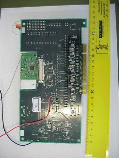
Click to zoom
Application Details
- Equipment Class
- DSS - Part 15 Spread Spectrum Transmitter
- Date of Grant
- Jul 18, 2001
- Application Purpose
- Original Equipment
- Date of Application
- Jul 18, 2001
- Equipment Note
- Wireless LAN Module
- Frequency Range
- 2412.00000000 - 2462.00000000
- Company
- Dynabook Inc.
- Country
- Japan
Documents & Files
Document Text
Text extracted from the exhibit documents filed with the FCC. Open a document above to read the original.
Users Manual
Installing Wireless LAN 1 / 3 Installing Wireless LAN To install the internal Wireless LAN, follow the procedures below. Removing the battery pack Before installing the Wireless LAN board, remove the battery pack. Installing the Wireless LAN board Before installing the Wireless LAN board, you will first have to remove the keyboard. Follow the steps below and refer to Figure 1 to Figure 5. 1. Turn the computer upside down. 2. Remove one screw securing the keyboard. Figure 1Removing one screw 3. Turn the computer rightside up and open the display cover. 4. Insert your fingernail or a thin object between under the rim of the keyboard brace and lift out the brace. Figure 2Removing the keyboard brace Installing Wireless LAN 2 / 3 5. Remove two screws securing the keyboard. 6. Rotate the keyboard out and lay it on the palm rest. Figure 3Removing the keyboard 7. Remove one screw securing the shield plate and lift out the plate. Figure 4Removing the shield plate 8. Connect the antenna cables to the Wireless LAN board. 9. Hold the board at about a 45 degree angle and insert it into PJ118 on the computer. Press the board carefully and firmly to ensure a solid connection. Installing Wireless LAN 3 / 3 10. Push the board down so that it lies flat and is secured by two latches. Figure 5Inserting the Wireless LAN board 11. Seat the shield plate and secure it with one screw. 12. Seat the keyboard and secure two screws. 13. Seat the keyboard holder and press to secure latches. 14. Turn the computer upside down and secure one screw. Installing the battery pack Install the battery pack. Toshiba Wireless LAN mini-PCI Card – Getting started 1-1 About Toshiba Wireless Solution 1 Wireless LAN Network Scenarios The Wireless LAN Card Kit enables you to: n Connect your computer to a Peer-to-Peer workgroup of wireless computing devices. n Connect your computer to a Local Area Network (LAN) Infrastructure that includes Wireless LAN Access Points, or other IEEE802.11 compliant LAN systems. n Expand the capabilities of your Wireless LAN Access Points, to support wireless devices that have been equipped with Wireless LAN Card. NOTE: The internal Wireless LAN Card can’t be used with the Toshiba Wireless LAN PC Card. Toshiba Wireless LAN mini-PCI Card – Getting started 1-2 Peer-to-Peer Workgroup The Peer-to-Peer workgroup configuration enables you to quickly set up a small wireless workgroup, where the workgroup participants can exchange files using features like “Files and Printer Sharing” as supported by Microsoft Networking. Figure 1-1Peer-to-Peer Wireless Workgroup You can use this option to setup a temporary or ad-hoc network in environments where no access points are available (for example in Small Office/Home Office (SOHO) environments). As long as the stations are within range of one another, this is the easiest and least expensive way to set up a wireless network. Toshiba Wireless LAN mini-PCI Card – Getting started 1-3 Enterprise Networking Figure 1-2Stand Alone Wireless LAN With the Wireless LAN Access Points you can connect to a corporate Local Area Network (LAN) infrastructure to have wireless access to all network facilities. LAN Infrastructures may either be. n Stand-alone wireless LANs as pictures in Figure 1-2 n Wireless network infrastructures connected to an existing Ethernet network as pictured in Figure 1-3. Toshiba Wireless LAN mini-PCI Card – Getting started 1-4 Figure 1-3LAN Infrastructure Toshiba Wireless LAN mini-PCI Card – Getting started 1-5 It’s Easy The Wireless LAN Card functions like any standard wired Ethernet card, but Wireless LAN does not need any wires! Where an Ethernet card requires a cable connection to a hub and/or patch panel, the cable physically ties you down to the location of the wired connection. Wireless LAN allows you connect your computer to a Local Area Network (LAN) system from anywhere within the wireless coverage area. Expanding or re-designing your network is easy: Add or relocate Wireless LAN Access Points, power-up your (new) Wireless LAN computers, and you’re done! Unlike Ethernet, Wireless LAN will enable you to roam throughout the network while remaining connected to the LAN. NOTE: The Wireless LAN Card is a radio product. Refer to the flyer “Information to the User” for regulatory information that may apply in your country. Toshiba Wireless LAN mini-PCI Card – Getting started 1-6 Wireless LAN Card Features Toshiba Wireless LAN mini-PCI Card is a wireless network card that fits into Mini PCI TypeIIIA. Toshiba Wireless LAN mini-PCI Card – Getting started 1-7 Wireless LAN Card Types The Wireless LAN Card is a wireless network card that complies with the IEEE 802.11 standard on wireless LANs (Revision B). The Wireless LAN Card supports data rates up to 11 Mbit/s. n Wi-Fi (Wireless Fidelity) certified by the Wireless Ethernet Compatibility Alliance (WECA). This means that your Wireless hardware will communicate with other vendors’ IEEE 802.11 compliant wireless LAN product. n Fully compatible with any other wireless LAN system based on Direct Sequence Spread Spectrum (DSSS) radio technology that complies with the “IEEE 802.11 standard on wireless LANs (Revision B). Toshiba Wireless LAN mini-PCI Card – Getting started 1-8 Wireless LAN Cards The Wireless LAN Card supports the following wireless LAN features: n Automatic Transmit Rate Select mechanism in the transmit range of 11, 5.5, 2 and 1 Mbit/s. n Frequency Channel Selection (2.4GHz). n Roaming over multiple channels. n Card Power Management. n Wired Equivalent Privacy (WEP) data encryption, based on the 128 bit RC4 encryption algorithm Toshiba Wireless LAN mini-PCI Card – Getting started 1-9 Finding Information This document was designed to give you a brief introduction about the Wireless LAN Card. In this document you will find the most important information to get your Wireless LAN network up and running, with a minimum set of parameters. Alternatively you can consult the on-line help documentation for the Wi…
Text truncated - open the document above for the full version.
Cover Letter(s)
Application CJ6PA3070WL Request for Limited Modular Approval Part 15 Unlicensed Modular Transmitter Approval Justification per DA 00-1407, released: June 26, 2000 RequirementReference 1. The modular transmitter must have its own RF shielding. See Exhibit 3 and Exhibit 9 2. The modular transmitter must have buffered modulation/data inputs All inputs to the modules are buffered through logic or microprocessor inputs. See Exhibit 5. 3. The modular transmitter must have its own power supply regulation. All power lines derived from the host device are regulated before energizing other circuits internal to the EUT. See Exhibit 5. 4. The modular transmitter must comply with the antenna requirements of Section 15.203 and 15.204(c). The EUT will be inbuild into host equipment, which has antenna built-in, which is inaccessible to the user. See Exibit 13 WL Usage 5. The modular transmitter must be tested in a stand-alone configuration, i.e., the module must not be inside another device during testing. Please refer to Exhibit 6 6. The modular transmitter must be labeled with its own FCC ID number, and, if the FCC ID is not visible when the module is installed inside another device, then the outside of the device into which the module is installed must also display a label referring to the enclosed module. The EUT carries an FCC ID label whose artwork and label position are clearly indicated; see Exhibit 1 exhibits. In addition the label for the host equipment is shown. 7. The modular transmitter must comply with any specific rule or operating requirements applicable to the transmitter and the manufacturer must provide adequate instructions along with the module to explain any such requirements. A copy of these instructions must be included in the application for equipment authorization. See Exhibit 12. 8. The modular transmitter must comply with any applicable RF exposure requirements. For example, FCC Rules in Sections 2.1091, 2.1093 and specific Sections of Part 15, including 15.319(i), 15.407(f), 15.253(f) and 15.255(g), require that Unlicensed PCS, UNII and millimeter wave devices perform routine environmental evaluation for RF Exposure to demonstrate compliance. In addition, spread spectrum transmitters operating under Section 15.247 are required to address RF Exposure compliance in accordance with Section 15.247(b)(4). RF output is 1 mW and constitutes no RF exposure hazard. RF Safety statements are provided in the Exhibit 13
External Photos
CETECOM ICT Services GmbH Test report nr..:2-2509-D/01Issue Date:20.06.01Page 68 (71) Pictures of the sample Picture 2: CETECOM ICT Services GmbH Test report nr..:2-2509-D/01Issue Date:20.06.01Page 69 (71) Pictures of the sample Picture 3: CETECOM ICT Services GmbH Test report nr..:2-2509-D/01Issue Date:20.06.01Page 70 (71) Pictures of the sample Picture 4: CETECOM ICT Services GmbH Test report nr..:2-2509-D/01Issue Date:20.06.01Page 71 (71) Pictures of the sample Picture 5:
ID Label/Location Info
Bottom side view Regulatory Label Regulatory Label of Wireless LAN on bottom of PC Regulatory Label on Mini PCI Wireless LAN Card xxxxx = Country of Manufacturing 14mm (ref.) 18.5mm (ref.) Country of Origin Label Label with S/N, P/N and MAC address Country of Origin label with BSMI number Mini PCI Label Placement (front side) Label with S/N, P/N and MAC address
Internal Photos
Application CJ6PA3070WL Exhibit 9: Internal Photographs Application CJ6PA3070WL Exhibit 9: Internal Photographs
Test Report
Measurement file output name is:5mbit.cnd Input command file name is:INPUT.CMDNote: 5.5 Mbit, 6 dB SIR tested for ( 15 dB SNR - 10.4 + 1 impl. losses). Input CW correction level:6dBTakes into account 1 dB of implementation loss (allowed 2 dB). Lowcount is:1000messages Only RxD errors are taken into account since these need better SIR then preamble at 1 MBit Highcount is:50000messagesAttention: Input the red cells for correct spreadsheet calculations!total errors45out of 280 measurement points. Rx level DUT is:-53dBmpercentage16,07% Number of received data errors as a function of frequency and interference levelOK?=<20%, OK Not measured combinations listed as "-1"HIJKLMNOPQRS Uncorrected Interference level dialed at CW generator -60-59-58-57-56-55-54-53-52RxD ErrorsPDARxD ErrorsPDABoth error True CW interference level at receiver input (dBm)detectedmissingdetectedmissingRxD and -66-65-64-63-62-61-60-59-58full testfull testup to CW AT CW PDA J/S ratio (dB)-13#PDA-12#PDA-11#PDA-10#PDA-9#PDA-8#PDA-7#PDA-6#PDA-5#PDArangerange=< -59 dBm= -59 dBm=< -59 dBm Frequency (Hz)(J/S = -5-1 dB)(J/S = -5-1 dB)timedate 24090000000100001000010000100001000010000100001000050000OK, 0 RxD errorsOK, No PDA errors00015:53:4915.04.99 24090500000100001000010000100001000010000100001000050000 OK, 0 RxD errorsOK, No PDA errors00015:52:1815.04.99 24091000000100001000010000100001000010000100001000050000OK, 0 RxD errorsOK, No PDA errors00015:50:4815.04.99 24091500000100001000010000100001000010000100001000050000OK, 0 RxD errorsOK, No PDA errors00015:49:1915.04.99 24092000000100001000010000100001000010000100001000050000OK, 0 RxD errorsOK, No PDA errors00015:47:4815.04.99 24092500000100001000010000100001000010000100001000050000OK, 0 RxD errorsOK, No PDA errors00015:46:1915.04.99 24093000000100001000010000100001000010000100001000050000OK, 0 RxD errorsOK, No PDA errors00015:44:4915.04.99 24093500000100001000010000100001000010000100001000050000 OK, 0 RxD errorsOK, No PDA errors00015:43:1815.04.99 24094000000100001000010000100001000010000100001000050000OK, 0 RxD errorsOK, No PDA errors00015:41:4915.04.99 24094500000100001000010000100001000010000100001000050000OK, 0 RxD errorsOK, No PDA errors00015:40:1815.04.99 24095000000100001000010000100001000010000100001000050000OK, 0 RxD errorsOK, No PDA errors00015:38:4815.04.99 24095500000100001000010000100001000010000100001000050000OK, 0 RxD errorsOK, No PDA errors00015:37:1815.04.99 24096000000100001000010000100001000010000100001000050000 OK, 0 RxD errorsOK, No PDA errors00015:35:4815.04.99 24096500000100001000010000100001000010000100001000050000OK, 0 RxD errorsOK, No PDA errors00015:34:1815.04.99 24097000000100001000010000100001000010000100001000050000OK, 0 RxD errorsOK, No PDA errors00015:32:4815.04.99 24097500000100001000010000100001000010000100001000050000 OK, 0 RxD errorsOK, No PDA errors00015:31:1715.04.99 24098000000100001000010000100001000010000100001000050000OK, 0 RxD errorsOK, No PDA errors00015:29:4715.04.99 24098500000100001000010000100001000010000100001000050000OK, 0 RxD errorsOK, No PDA errors00015:28:1715.04.99 24099000000100001000010000100001000010000100001000050000 OK, 0 RxD errorsOK, No PDA errors00015:26:4615.04.99 24099500000100001000010000100001000010000100001000050000OK, 0 RxD errorsOK, No PDA errors00015:25:1615.04.99 24100000000100001000010000100001000010000100001000050000OK, 0 RxD errorsOK, No PDA errors00015:23:4515.04.99 24100500000100001000010000100001000010000100001000050000 OK, 0 RxD errorsOK, No PDA errors00015:22:1515.04.99 24101000000100001000010000100001000010000100001000050000OK, 0 RxD errorsOK, No PDA errors00015:20:4515.04.99 24101500000100001000010000100001000010000100001000050000OK, 0 RxD errorsOK, No PDA errors00015:19:1415.04.99 24102000000100001000010000100001000010000100001000050000 OK, 0 RxD errorsOK, No PDA errors00015:17:4415.04.99 24102500000100001000010000100001000010000100001000050000OK, 0 RxD errorsOK, No PDA errors00015:16:1415.04.99 24103000000100001000010000100001000010000100001000050000OK, 0 RxD errorsOK, No PDA errors00015:14:4315.04.99 24103500000100001000010000100001000010000100001000050000 OK, 0 RxD errorsOK, No PDA errors00015:13:1315.04.99 24104000000100001000010000100001000010000100001000050000OK, 0 RxD errorsOK, No PDA errors00015:11:4215.04.99 24104500000100001000010000100001000010000100001000050000OK, 0 RxD errorsOK, No PDA errors00015:10:1215.04.99 24105000000100001000010000100001000010000100001000050000 OK, 0 RxD errorsOK, No PDA errors00015:08:4215.04.99 24105500000100001000010000100001000010000100001000050000 OK, 0 RxD errorsOK, No PDA errors00015:07:1215.04.99 24106000000100001000010000100001000010000100001000050000 OK, 0 RxD errorsOK, No PDA errors00015:05:4215.04.99 24106500000100001000010000100001000010000100001000050000OK, 0 RxD errorsOK, No PDA errors00015:04:1215.04.99 24107000000100001000010000100001000010000100001000050000OK, 0 RxD errorsOK, No PDA errors00015:02:4215.04.99 24107500000100001000010000100001000010000100001000050000 OK, 0 RxD errorsOK, No PDA errors00015:01:1115.04.99 24108000000100001000010000100001000010000100001000050000OK, 0 RxD errorsOK, No PDA errors00014:59:4115.04.99 24108500000100001000010000100001000010000100001000050000OK, 0 RxD errorsOK, No PDA errors00014:58:1115.04.99 24109000000100001000010000100001000010000100001000050000 OK, 0 RxD errorsOK, No PDA errors00014:56:4215.04.99 24109500000100001000010000100001000010000100001000050000OK, 0 RxD errorsOK, No PDA errors00014:55:1115.04.99 24110000000100001000010000100001000010000100001000050000OK, 0 RxD errorsOK, No PDA errors00014:53:4115.04.99 24110500000100001000010000100001000010000100001000050000 OK, 0 RxD errorsOK, No PDA errors00014:52:1015.04.99 24111000000100001000010000100001000010000100001000050000 OK, 0 RxD errorsOK, No PDA errors00014:50:4115.04.99 24111500000100001000010000100001000010000100001000050000OK, 0 RxD errorsOK, No PDA errors00014:49:1115.04.99 24112000000100001000010000100001000010000100001000050000OK, 0 RxD erro…
Text truncated - open the document above for the full version.
Test Report
CETECOM ICT Services GmbH Test report nr.:2-2509-D/01Issue date:20.06.01Page 1 (71) Test report no.: 2-2509-D/01 FCC Part 15.247 Toshiba Wireless LAN Card PA3070U-1MCP Accredited Testing Laboratory DAR-Registration number: TTI-P-G 166/98-10 CETECOM ICT Services GmbH Test report nr.:2-2509-D/01Issue date:20.06.01Page 2 (71) Table of Contents 1 General information 1.1 Notes 1.2 Testing laboratory 1.3 Details of applicant 1.4 Application details 1.5 Test item 1.6 Test standards 2 Technical test 2.1 Summary of test results 2.2 Test report 1 General information 1.1 Notes The test results of this test report relate exclusively to the test item specified in 1.5. The CETECOM ICT Services GmbH does not assume responsibility for any conclusions and generalisations drawn from the test results with regard to other specimens or samples of the type of the equipment represented by the test item. The test report may only be reproduced or published in full. Reproduction or publication of extracts from the report requires the prior written approval of the CETECOM ICT Services GmbH. 1.2Testing laboratory CETECOM ICT Services GmbH 66117 Saarbrücken Untertürkheimer Straße 6 - 10 Deutschland Telefone: + 49 681 598 - 0 Telefax : + 49 681 598 - 9075 E-mail : [email protected] Internet : www.cetecom.de Accredited testing laboratory DAR-registration number : TTI-P-G 166/98-00 CETECOM ICT Services GmbH Test report nr.:2-2509-D/01Issue date:20.06.01Page 3 (71) 1.3Details of applicant Name : Technology & Quality Management Division, Toshiba Corporation, Digital Media Network Company Street : 1-1-1 Shibaura City : Minarto-ku, Tokyo 198-8001 Country : Japan Telephone : +81 (3) 3457 2565 Telefax : +81 (3) 5444 9404 Contact : Mr. Hideo Abe Telephone : +81 (3) 3457 2565 1.4Application details Date of receipt of application : 10.06.01 Date of receipt of test item : 10.06.01 Date of test : 19. – 20.06.01 1.5Test item Type of equipment : WLAN Module for laptops (Mini PCI card) Type designation:PA3070U-1MCP Manufacturer: - applicant - Street: City: Country: Serial number:MAC: 00022D1221BB Additional informations: : Frequency:2400 – 2483.5 MHz (here 2412 – 2462 MHz) Type of modulation:22M0P7D (DSSS) Number of channels :11 Antenna:integral antennas Power supply:3.3V DC powered by PC / Laptop Output power cond.max:83.2 mW Type of equipment:Class B Temperature range :+5°C - +35°C 1.6Test standards: FCC Part 15 §15.247 CETECOM ICT Services GmbH Test report nr.:2-2509-D/01Issue date:20.06.01Page 4 (71) 2 Technical test 2.1Summary of test results The antenna gain measurement was performed by the difference between conducted and radiated output measurement. All measurement settings were according to FCC 15.35, 15.209, 15.247 and the „Guidance on measurement for DSSS systems“. The settings for RBW, VBW and sweeptime are according to FCC requirements. The radiated measurements were performed with a Toshiba Laptop Satellite 1800, the conducted and extreme tests were performed with an extender card in a Desktop PC. For processing gain see separate paper provided by LUCENT. Technical responsibility for area of testing : 18.07.01RSC 8411 Berg DateSectionNameSignature Technical responsibility for area of testing : 20.06.01RSC8414Ames DateSectionNameSignature CETECOM ICT Services GmbH Test report nr.:2-2509-D/01Issue date:20.06.01Page 5 (71) 2.2Testreport TEST REPORT Testreport no. : 2-2509-D/01 CETECOM ICT Services GmbH Test report nr.:2-2509-D/01Issue date:20.06.01Page 6 (71) TEST REPORT REFERENCE LIST OF MEASUREMENTS ParagraphPARAMETER TO BE MEASUREDPAGE Transmitter parameters § 15.247 (a)(2) Spectrum Bandwitdh of a DSSS System 7 §15.231 (d)Frequency stability11 § 15.247 (b)(1) Maximum peak output power13 § 15.247 (c)(1) Emission limitations 21 § 15.247 (d)Power Spectral Density51 § 15.247 (e)Processing Gain of DSSS System55 § 15.107Conducted emissions56 Receiver parameters § 15.209Spurious radiations - Radiated58 Test equipment listing61 Photographs of the equipment63 CETECOM ICT Services GmbH Test report nr..:2-2509-D/01Issue Date:20.06.01Page 7 (71) Equipment under test : WLAN Module Ambient temperature : 21° °° °C Relative humidity : 51% REFERENCE NUMBER(S) OF TEST EQUIPMENT USED (for reference numbers see test equipment listing) 64 SPECTRUM BANDWITH OF DSSS-SYSTEMSUBCLAUSE § 15.247 (a)(2) TEST CONDITIONS6 dB BANDWIDTH ( kHz ) Frequency (MHz)241224422462 T nom ( 20 )° °° °C V nom ( 3.3 )V1022095699719 Measurement uncertainty±3dB RBW = 100 KHz, Span >> RBW, here 25 MHz LIMIT SUBCLAUSE §15.247(a) (2) The minimum 6dB bandwith shall shall be at least 500 KHz CETECOM ICT Services GmbH Test report nr..:2-2509-D/01Issue Date:20.06.01Page 8 (71) Equipment under test : WLAN Module Ambient temperature : 21° °° °C Relative humidity : 51% REFERENCE NUMBER(S) OF TEST EQUIPMENT USED (for reference numbers see test equipment listing) 64 SPECTRUM BANDWITH OF DSSS-SYSTEMSUBCLAUSE § 15.247 (a)(2) 2412 MHz A Unit dBm RBW 100 kHz VBW 100 kHz SWT 6.5 ms 22 dB Offset22 dB Offset Ref Lvl 12 dBm Ref Lvl 12 dBm RF Att 20 dB 2.5 MHz/Center 2.412 GHzSpan 25 MHz 1VIEW1MA -80 -70 -60 -50 -40 -30 -20 -10 0 10 1 1 2 Marker 1 [T1] 2.87 dBm 2.41362826 GHz 1 [T1] 2.87 dBm 2.41362826 GHz 1 [T1] -6.58 dB -6.61322645 MHz 2 [T1] -5.99 dB 3.60721443 MHz REF -3.1 dBm Date: 20.JUN.2001 15:13:00 RBW = 100 KHz, Span >> RBW, here 25 MHz LIMIT SUBCLAUSE §15.247(a) (2) The minimum 6dB bandwith shall shall be at least 500 KHz , here 8.317 MHz CETECOM ICT Services GmbH Test report nr..:2-2509-D/01Issue Date:20.06.01Page 9 (71) Equipment under test : WLAN Module Ambient temperature : 21° °° °C Relative humidity : 51% REFERENCE NUMBER(S) OF TEST EQUIPMENT USED (for reference numbers see test equipment listing) 64 SPECTRUM BANDWITH OF DSSS-SYSTEMSUBCLAUSE § 15.247 (a)(2) 2442 MHz A Unit dBm RBW 100 kHz VBW 100 kHz SWT 6.5 ms 22 dB Offset22 dB Offset Ref Lvl 12 dBm Ref Lvl 12 dBm RF Att 20 dB Center 2.442 GHzSpan 25 MHz2.5 MHz/ 1VIEW1MA -80 -70 -60 -50 -40 -30 -20 -10 0 10 1 1…
Text truncated - open the document above for the full version.
Test Report
Lucent Technologies Bell Labs Innovations Zade!stede 1-10 3431 JZ Nieuwegein The Netherlands Phone: +3! 306097666 Fax: +3! 306097556 Nieuwegein, 30 May 2001 Re: Processing Gain WaveLANIOrinoco PC Cards Add. Info to Processing Gain report: For Chi Is bol rate etc. see the table below: Bit rate Chip/symbol rate Bit/symbol rate ChiD/bit rate Extra Information: 1. For 1 and 2 Mbp/s OQPSK modulation using a fixed spreading sequence the symbol rate is 1 MSymbol/s. The symbol length is 11 chips. Each chip duration is 1/11 uS. A symbol duration is 1 uS. The chip/symbol rate is 11. The theoretical process gain is 1 O*LOG{11 ) = 10 dB. 2. For 5.5 and 11 Mbp/s CCK where the spreading sequence is a function of the transmitted data, the symbol rate is 8/11 MSymbol/s. The symbol length is 8 chips. Each chip duration is 1/11 uS. A symbol duration is 8/11 uS. The chip/symbol rate is 8. The theoretical process gain is 1 O*LOG(8) = 9 dB. Due to the fact that only 256 code sequences out of the 65536 code sequences that are available are used, there is coding gain. Therefore the processing gain of a CCK system consists of spreading gain and coding gain together. As such a CCK system does meet the FCC requirement for a process gain of minimal 1 a dB. Explanation: The Lucent High Speed modulation is compliant to draft standard extension IEEE 802.11 b for 5.5 and 11 MBitls signaling rates. For this modulation technique the Symbol length is 8 Chips (1 Symbol duration equals 8111 uS). However, the 8 Chips are not a fixed spreading sequence as is the case for the 1 and 2 MBitls modulation technique. These 8 Chips, applied in a OPSK modulation, use 256 unique patterns out of the 65536 different possible patterns, wherebyeach pattern represents a specific data sequence (4 or 8 bits). Thus this type of modulation introduces Coding Gain, since only 256 patterns are used out of 65536 possible combinations. Therefore it can be concluded that the system employs Coding Gain in addition to Spreading Gain. The Processing Gain of the system is taken as the combined result of Coding and Spreading Gain, so a Processing Gain of 10 dB can be met with 8 Chips per Symbol. Lucent has shown bya CW jammer margin test that a SIR of 10 dB can be met, while meeting the system specified BER. It is our understanding that this is compliant with the FCC ruling. Therefore the test report shows that the Lucent product, operating at l' 2, 5.5 and 11 Mbitls meets a Processing Gain of at least 10 dB, under the conditions as specified by the FCC. Sincerel y yours, ~ Bert Vos, CertiUns Support,
Test Report
Nederland B.V. WCND FCC ID: WLPC24H/WLPCE24HReport No. 011734, Rev. B TEST REPORT Subject: Processing Gain For WaveLAN IEEE PC CARD type 2 HS Ref.: FCC Rules 47 CFR Part 15, Section 5.247d Report Prepared by: Maarten Visee May 6, 1999 NameSignatureDate Concurrence: 1. Director of Engineering Bruce Tuch May 6, 1999 NameSignatureDate 2. Team Captain Frans Hoekstra May 6, 1999 NameSignatureDate FCC Processing Gain Measurements Results, FCCID WLPC24H/WLPCE24H, Report No. 011734, Rev. B. Lucent WCND Confidential ©1999 2 Lucent WCND Confidential Information ©1999 FCC Processing Gain Measurements Results, FCCID WLPC24H/WLPCE24H, Report No. 011734, Rev. B. Lucent WCND Confidential ©1999 i DateSectionDescription 04/16/99 , Rev. A Initial release. 05/6/99, Rev. B 2Changed spreading gain into processing gain. 4.1For data rates of 5.5 and 11 Mbit/s changed processing gain requirements of 9 dB into 10 dB. 4.2Changed description for demodulated data availability at the interconnection between RF and DSP into the interconnection between DSP and digital circuits. Changed spreading gain into processing gain. 7.2, 7.3 Changed sub sections Measurement Results and Measurement Conclusion. Annex AUpdated flow chart. Change History: FCC Processing Gain Measurements Results, FCCID WLPC24H/WLPCE24H, Report No. 011734, Rev. B. Lucent WCND Confidential ©1999 1 This document describes the Receiver Processing Gain verification measurements performed at the WaveLAN-II PC- Card Type 2, according to Ref.[2]. The Lucent WaveLAN-II PC-Card Type 2 product confirms to the minimum required 10 dB processing gain, as set forth by the FCC for operation in the 2.4 GHz ISM band. 1- Document FCC 97-114, Appendix C, Guidance on Measurements for Direct Sequence Spread Spectrum Systems. 2- Hardware Functional Specification for WaveLAN-II Embedded, High Speed, Doc. No. 011735, Rev. A, Source Organization Lucent Technologies WCND Utrecht. 3-Viterbi, A. J., Principles of Coherent Communications, New York, McGraw-Hill 1966. 4- Proakis, J.G., Digital Communications, New York, McGraw-Hill 1989, page 270. 4.1 Test introduction - FCC requirements: Part of FCC certification for the Lucent WaveLAN IEEE 802.11 High Speed compliant Network Interface Card (NIC) is a processing gain test. This test proves that the receiver of the tested product employs a true spread spectrum device receiver structure, taking full advantage of the direct sequence spread spectrum modulation technique. This test verifies the receiver processing gain to be 10 dB or more for a data rate of 1, 2, 5.5 and 11 Mbit/s, by monitoring the Bit Error Rate (BER) of the product under test for each data rate, while operating under strict defined received signal conditions. Several methods of showing compliance to the rules are possible, from a stepped CW jammer to a continuous sweeping CW interferer. For this test the discrete stepped CW jammer method was chosen, as described in Ref.[1]. 1.Summary: 2.Conclusion: 3.References: 4.Measurement description: FCC Processing Gain Measurements Results, FCCID WLPC24H/WLPCE24H, Report No. 011734, Rev. B. Lucent WCND Confidential ©1999 2 Therefore a receiver input signal is applied to the product under test, in the presence of a Continuous Wave (CW) interference source, also referred to as CW jammer. The test takes place at the product Functional Specification (Ref.[2]) specified conditions for BER rate measurements, specifying a BER equal or better than 10^-8 at a receiver input level of -55 dBm. For practical reasons these test are performed at -55 dBm or -53 dBm. This small deviation from the Functional Specification should not cause any deviation from the specified Bit Error Rate, since the received levels are well above the thermal noise. The test criteria for meeting the minimal processing gain is such that it takes the theoretical calculated SNR for the applied modulation technique and specified BER as a reference. From this given SNR the processing gain is subtracted, yielding the CW Jammer to Signal ratio J/S. From Ref. [4], likewise as Ref.[3] consulted in Ref. [1], it is determined that for a BER of 10^-8 the SNR (S/N)o equals: 13 dB @ 1 Mbit/s, 15 dB @ 2 Mbit/s, 15 dB @ 5.5 Mbit/s, 18 dB @ 11 Mbit/s. Thus the J/S ratio for a processing gain of 10 dB that must be met is calculated as: -13 + 10 = -3 dB @ 1 Mbit/s (DBPSK), -15 + 10 = -5 dB @ 2 Mbit/s (DQPSK), -15 + 10 = -5 dB @ 5.5 Mbit/s (CCK), -18 + 10 = -8 dB @ 11 Mbit/s (CCK). Two types of measurement corrections are allowed for as described in Ref.[1]. The first taking into account 2 dB implementation losses, thus increasing the absolute J/S ratio by 2 dB. The second correction allows for deleting the 20% worst-case frequencies in the processing gain test that causes the test at that CW interference to fail. This implies that for the considered 14 MHz wide measurement interval the worst case 57 CW jammer frequencies can be ignored, being those that result in received data FCC Processing Gain Measurements Results, FCCID WLPC24H/WLPCE24H, Report No. 011734, Rev. B. Lucent WCND Confidential ©1999 3 errors/missing frames (20% of 14 MHz *(1 MHz/50 KHz) + 1 = (20% * 281) + 1 = 57). FCC Processing Gain Measurements Results, FCCID WLPC24H/WLPCE24H, Report No. 011734, Rev. B. Lucent WCND Confidential ©1999 4 4.2 Test sequence: The measurements are performed at a 50 KHz CW jammer raster. For each CW jammer frequency 10^8 bits are transmitted by the reference transmitter, and received by the product under test. For practical reasons 50.000 messages are transmitted. After blanking out frame overhead 1927 bits per frame are monitored. This results in 50.000 * 1927 = 9650000 transmitted bits for a BER test, which is a mere 1.4% less than the targeted 10^8 bits. Though it would be more elegant to show BER compliance for at least say ten times 10^8 transmitted/received bits, the time involved with this grows significantly. Since the CW interferer is stepped in a 50 KHz raster, covering the rec…
Text truncated - open the document above for the full version.
Test Setup Photos
CET…
Text truncated - open the document above for the full version.
Contact Information
Applicant
Ryuichi Kamimura(Senior Manager)
Technical Contact
Non-Technical Contact
CETECOM GmbHThorsten Stebenau
[email protected]+4920549519974
Test Firm
CETECOM GmbHWolfgang Richter
Technical Specifications
| # | Rule Parts | Frequency Range | Power Output |
|---|---|---|---|
| 1 | 15C | 2.41 GHz - 2.46 GHz | 83.20 mW |
Other Applications from Dynabook Inc.
CJ6PA5347RT
Oct 20, 2022dynabook Wireless Optical Silent Mouse
Equipment Class
DXX - Part 15 Low Power Communication Device Transmitter
CJ6PYT0XPC
Apr 28, 2021Notebook Computer
Equipment Class
DSS - Part 15 Spread Spectrum Transmitter
CJ6UPA5238WL
Sep 01, 2015dynadock WiAC
Equipment Class
NII - Unlicensed National Information Infrastructure TX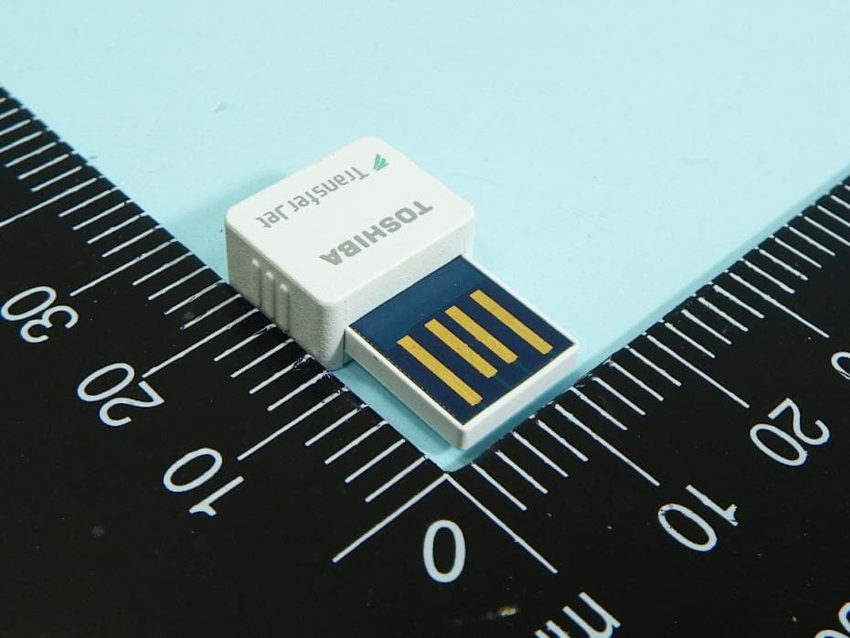
CJ6UPA5144TJ
Aug 07, 2014TransferJet USB Adapter
Equipment Class
JBP - Part 15 Class B Computing Device Peripheral
CJ6UPA5145TJ
Aug 07, 2014TransferJet MicroUSB Adapter
Equipment Class
UWB - Ultra Wideband Transmitter