CJ6PT820WLWireless LAN
Dynabook Inc.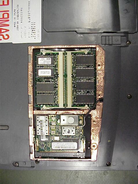
Click to zoom
Application Details
- Equipment Class
- DSS - Part 15 Spread Spectrum Transmitter
- Date of Grant
- Dec 06, 2000
- Application Purpose
- Original Equipment
- Date of Application
- Dec 06, 2000
- Equipment Note
- Wireless LAN
- Frequency Range
- 2412.00000000 - 2462.00000000
- Company
- Dynabook Inc.
- Country
- Japan
Documents & Files
Document Text
Text extracted from the exhibit documents filed with the FCC. Open a document above to read the original.
Users Manual
Toshiba Wireless LAN mini-PCI Card – Getting started Information to the User Wireless Interoperability The Toshiba Wireless LAN Mini PCI Card products are designed to be interoperable with any wireless LAN product that is based on Direct Sequence Spread Spectr um(DSSS) radio technology, and is compliant to: •The IEEE 802.11 Standard on Wireless LANs(Revision B), as defined and approved by the Institute of Electrical and Electronics Engineers. •The Wireless Fidelity(WiFi) certification as defined by the WECA Wireless Ethernet Compatibility Alliance. Wireless LAN and your Health Wireless LAN products, like other radio devices, emit radio frequency electromagnetic energy. The level of energy emitted by Wireless LAN devices however is far much less than the electromagnetic energy emitted by wireless devices like for example mobile phones. Because Wireless LAN products operate within the guidelines found in radio frequency safety standards and recommendations, Toshiba believes Wireless LAN is safe for use by consumers. These standards and recommendations reflect the consensus of the scientific community and result from deliberations of panels and committees of scientists who continually review and interpret the extensive research literature. In some situations or environments, the use of Wireless LAN may be restricted by the proprietor of the building or responsible representatives of the organization. These situations may for example include: • Using the Wireless LAN equipment on board of airplanes, or • In any other environment where the risk of interference to other devices or services is perceived or identified as harmful. If you are uncertain of the policy that applies on the use of wireless devices in a specific organization or environment (e.g. airports), you are encouraged to ask for authorization to use the Wireless LAN device prior to turning on the equipment. Toshiba Wireless LAN mini-PCI Card – Getting started Regulatory Information The Toshiba Wire le ss LAN Mini PCI Card must be installed and used in strict accordance with the manufacturer’s instructions as described in the user documentation that comes with the product. This device complies with the following radio frequency and safety standards. Canada – Industry Canada (IC) This device complies with RSS 210 of Industry Canada. Operation is subject to the following two conditions: (1) this device may not cause interference , and (2) this device must accept any interference, including interference that may cause undesired operation of this device.” L ‘ utilisation de ce dispositif est autorisée seulement aux conditions suivantes : (1) il ne doit pas produire de brouillage et (2) l’ utilisateur du dispositif doit étre prét à accepter tout brouillage radioélectrique reçu, même si ce brouillage est susceptible de compromettre le fonctionnement du dispositif. Europe – EU Declaration of Conformity This device complies with the essential requirements of the R&TTE Directive 1999/5/EC with essential test suites as per standards: • EN 60950 Safety of Information Technology equipment • ETS 300 328 Technical requirements for radio equipment • ETS 300 826 General EMC requirements for radio equipment. For outdoor usage only channel 10 (2457 MHz) and 11 (2462 MHz) is allowed. For private usage outside buildings across public grounds over less than 300m no special registration with IBPT/BIPT is required. Registration to IBPT/BIPT is required for private usage outside buildings across public grounds over more than 300m. An IBPT/BIPT license is required for public usage outside building. For registration and license please contact IBPT/BIPT. Gebruik buiten gebouw alleen op kanalen 10 (2457 MHz) en 11 (2462 MHz). Voor privé-gebruik buiten gebouw over publieke groud over afstand kleiner dan 300m geen registratie bij BIPT/IBPT nodig; voor gebruik over afstand groter dan 300m is wel registratie bij BIPT/IBPT nodig. Voor publiek gebruik buiten gebouwen is licentie van BIPT/IBPT verplicht. Voor registratie of licentie kunt u contact opnemen met BIPT. België/ Belgique: L’utilisation en extérieur est autorisé sur le canal 10 (2457 MHz) et 11 (2462 MHz). Dans le cas d’une utilisation privée, à l’extérieur d’un bâtiment, au-dessus d’un espace public, aucun enregistrement n’est nécessaire pour une distance de moins de 300m. Pour une distance supérieure à 300m un enregistrement auprès de I’IBPT est requise. Pour une utilisation publique à I’extérieur de bâtiments, une licence de I’IBPT est requise. Pour les enregistrements et licences, veuillez contacter I’IBPT. License required for outdoor installations. Check with reseller for procedure to followDeutschland : Anmeldung im Outdoor-Bereich notwendig, aber nicht genehmigungspflichtig. Bitte mit Händler die Vorgehensweise abstimmen. Restricted frequency band: only channels 10 and 11 (2457 MHz and 2462 MHz respectively) may be used in France. License required for every installation, indoor and outdoor installations. Please contact ART for procedure to follow. France: Bande de fréquence restreinte : seuls les canaux 10 à 11 (2457 et 2462 MHz respectivement) doivent être utilisés en France. Toute utilisation, qu’elle soit intérieure ou extérieure, est soumise à autorisation. Vous pouvez contacter I’Autorité de Régulation des Télécommuniations (http://www.art-telecom.fr) pour la procédure à suivre. License required for indoor use. Use with outdoor installations not allowedItalia: E’necessaria la concessione ministeriale anche per l’uso interno. Verificare con i rivenditori la procedura da seguire. L’uso per installazione in esterni non e’ permessa. License required for outdoor installations. Check with reseller for procedure to followNederland Licentie verplicht voor gebruik met buitenantennes. Neem contact op met verkoper voor juiste procedure Toshiba Wireless LAN mini-PCI Card – Getting started USA-Federal Communications Commission(FCC) This device complies with Part 15 of FCC Rules. Operation of the devices i…
Text truncated - open the document above for the full version.
Cover Letter(s)
Exhibit 13: Cover Letters December 7, 2000 FEDERAL COMMUNICATIONS COMMISSION Equipment Authorization Division 7435 Oakland Mills Road Columbia, MD 21046 To Whom It May Concern: Enclosed is the documentation for a spread spectrum transmitter operating under FCC Part 15, Subpart C, Section 15.247. This application was certified by Communication Certification Laboratory (CCL) under the TCB (Scope A4) program. The applicant, model number and FCC ID are listed below: Applicant: Toshiba Corporation, Product Safety Group Model: PT820 FCC ID: CJ6PT820WL Please let me know if I can be of further assistance. Sincerely yours, COMMUNICATION CERTIFICATION LABORATORY Joseph W. Jackson V.P. Marketing
External Photos
Photo documentation Toshiba TECRA 8200 Test sample complete Power supply downside Floppy downside Floppy upside Lasptop upper side Laptop left side Laptop back side Laptop right side Laptop lower side Laptop sign Laptop display Laptop lower side Cover open view to LAN module
ID Label/Location Info
LABEL INFORMATION (for Wireless LAN model) and (for no Wireless LAN model) Rating Label
Internal Photos
Laptop lower side Cover open view to LAN module LAN modul upper side LAN module lower side Display without cover Antenna placement (Antenna is the same as used in Satellite Pro 4600) Antenna view backside (Antenna is the same as used in Satellite Pro 4600)
Internal Photos
Exhibit 9 - supplemental32-0017 Page 1 of 8Toshiba TECRA 8200 with Wireless LAN mini PCI card Mini PCI Wireless LAN board - lower side with shield Exhibit 9 - supplemental32-0017 Page 2 of 8Toshiba TECRA 8200 with Wireless LAN mini PCI card Mini PCI Wireless LAN board - lower side without shield Exhibit 9 - supplemental32-0017 Page 3 of 8Toshiba TECRA 8200 with Wireless LAN mini PCI card Mini PCI Wireless LAN board - upper side with shield Exhibit 9 - supplemental32-0017 Page 4 of 8Toshiba TECRA 8200 with Wireless LAN mini PCI card Mini PCI Wireless LAN board - upper side without shield Exhibit 9 - supplemental32-0017 Page 5 of 8Toshiba TECRA 8200 with Wireless LAN mini PCI card Antenna board, top side Exhibit 9 - supplemental32-0017 Page 6 of 8Toshiba TECRA 8200 with Wireless LAN mini PCI card Antenna board, bottom side Exhibit 9 - supplemental32-0017 Page 7 of 8Toshiba TECRA 8200 with Wireless LAN mini PCI card Location of antenna and cabling to antenna Exhibit 9 - supplemental32-0017 Page 8 of 8Toshiba TECRA 8200 with Wireless LAN mini PCI card Antennas visible at top of LCD display
Operational Description
DESCRIPTION OF THE Orinoco 2.4 GHz BLOCKDIAGRAM The various parts of the Blockdiagram are numbered and an explanation is given of these blocks. First the transmitter will be described: A) Digital Signal Processor. (22) Function : Generate spreaded signal with an Barker sequence of 11, the original raw data rate of two Megabits is transformed to a symbol rate of one MegaBaud and multiplied with eleven and modulated with a DQPSK ( Differential Quadrature Phase Shift Keying ) Modulation. The unfiltered data comes out of I and Q and goes to the up/down mixer (6) B) The above signals are mixed in (6) in a so called quadrature modulator with the Intermediate Frequency ( IF) of 352 MHz. C) The upmixer is fed by the VCO of 704 MHz, which is divided by 2 to 352 MHz. D) The SAW ( 8 ) filters all unwanted mixing products, such that only the 352 MHz band remains. E) This signal goes into the RF upmixer ( 9) SA2420 were it is mixed with the RF VCO with a range of 2050 to 2150 MHz. F) The Rx/Tx switch (17) brings the signal to the variable attenuator (10 ), where the output level is controlled. G) The signal is fed through a 2.4- 2.5 GHz bandpass filter (11) to remove all unwanted mixer products, and thus to get a clean signal for further processing. H) The signal is amplified in (12), with approx 23 dB to an output level of approx. 15 dBm I) This signal goes to the special connector. J) The output power is controlled with a so called power feed back loop (15) in which the output power is compared with a DAC value from (10) Receiver functions. K) The receive signal enters the antenna passes the RX/TX switch (14) and (13) this is set to RX mode. L) The signal goes through the 2.4 GHz filter (16) to remove all unwanted spectral components in order to deliver a clean signal for the receiver. M) A Low Noise Amplifiers (LNA) (in 9) is used to amplify the weak signal to a level fitted for down mixing. N) The AGC (27) can amplify or attenuate the signal according to the Digital signal processor required input with a step size of 26 dB. O) Again the Rx/Tx switch in the Rx mode is passed and also the same filter as in transmit mode ( 18). P) The down mixer (9) mixes the 2.4 GHz with the 2.1 GHz to the 352 MHz IF. Q) The signal of 352 MHz is amplified again (9) and filtered by a SAW filter (19) to give a clean signal for the second mixer. R) The Downmixer (6) mixes the 352 MHz signal down to the I and Q signals, also the auto gain control can increase the level to the required level via line 20. S)The very low amplitude baseband I and Q signal is amplified in the AMPs (6) to a level fitted for the Analog to Digital converters (22), which make it a proper signal for the digital signal processor. T) The digital signal processor (22) removes the spreading as present on the signal with a so called autocorrelation function. The resulting output of the processor is a received data rate of 2 Megabits. VCO , PLL and OSC. U)These three form one entity to generate a single tone signal for down mixing. There are two of these blocks available, one for the IF LO (7 and 6 ) (352MHz ) and one for the RF LO (25 and 26) of 2050 to 2150 MHz. V)All the PLL’s and the processor (2) have one reference Crystal of 22 MHz (4) with an accuracy of 25 ppm. General circuits: W)Antenna Diversity. Depending on the signal strength and signal quality the Digital processor (22) can select between two antenna’s which gives the best signal. This is done initial during the training sequence in the received signal. X)Automatic Gain control. Depending on the signal strength and signal quality the Digital processor (22) can choose to increase or decrease the signal level at the digital input, this is done by reducing or increasing the gain in the receiver via the LNA-AGC (in 9). Y) The Signal processor (22) can read via the MAC (2) the registers for programming all Z) The MAC is used to do the handshaking with the miniPCI bridge chip bus (1 ) and handling the IEEE protocol. Also used to load the PLL frequencies and dividers, also used to interface to the Eeprom which contains all parameters for the PLL’s and the Callcode Blockdiagram description of the Lucent 2.4 GHz Orinoco, miniPCI card Guus Jansen Aug 16, 2000 U\D MIXER VCO PLL D A D A I Q RX/TX SWITCH DIG SIG PROC BANDPASS FILTER LNA/ AGC UP MIXER DOWN MIXER RFCONNECTOR(S) & DIVERSITY SWITCH AUTOMATIC GAIN CONTROL ANTENNA DIVERSITY CONTROL 2.4-2.5GHz 2.05-2.15GHz I Q PLL VCO RX/TX SWITCH RX/TX SWITCH BANDPASS FILTER refoscand load osc load Amp PFB 352MHz saw D A D A MAC SRAM 128k x 8 32k x 8 70ns 3.3 V Xtal BANDPASS FILTER 704 MHz 352MHz saw 200nS 3.3 V FLASH ROM H E R M E S T H E S E U S miniPCI bridge bus 1 2 3 22 6 7 8 19 9 10 11 15 14 12 13 18 16 21 20 4 5 17 22MHz 25 26 27 9 BlockdiagrammLucent 2.4GHz WaveLAN
RF Exposure Info
Exhibit 11: RF Exposure/Environmental Evaluation Section 15.247 (b)(4) Requirement: Spread spectrum devices shall be operated in a manner that ensures that the public in not exposed to radio frequency energy levels in excess of the Commission’s guidelines. See § 1.1307(b)(1) and 2.1093 of this chapter. All equipment shall be considered to operate in a “general population/uncontrolled” environment. Applications for equipment authorization of devices operating under this section must contain a statement confirming compliance with these requirements for both fundamental emissions and unwanted emissions. Technical information showing the basis for this statement must be submitted to the Commission upon request. Demonstration of Compliance: The Satellite Pro 4600 is classified as a portable device, which is designed so that a minimum separation distance of 5.0 centimeters is maintained between the transmitter’s radiating structure and the body of the user or nearby persons, and it does not operate in the one of the services listed in § 2.1093(c). Therefore, the Satellite Pro 4600 is categorically excluded from routine environmental evaluation for RF exposure as per § 2.1093(c). The user’s manual contains a warning statement that instructs the user that the 5.0 centimeter separation distance must be maintained in order to comply with the RF exposure requirement. Sample of RF Exposure Statement: Caution: Exposure to Radio Frequency Radiation. The radiated output power of the Toshiba Wireless LAN Mini PCI Card is far below the FCC radio frequency exposure limits. Nevertheless, the Toshiba Wireless LAN Mini PCI Card shall be used in such a manner that the potential for human contact during normal operation is minimized. When using this device in combination with Wireless LAN Outdoor Antenna products, a certain separation distance between antenna and nearby persons has to be kept to ensure RF exposure compliance. The distance between the antennas and the user should not be less than 5.0 cm. Refer to the Regulatory Statements as identified in the documentation that comes with those products for additional information. The Toshiba Wireless LAN Mini PCI Card is far below the FCC radio frequency exposure limits. Nevertheless, it is advised to use the Toshiba Wireless LAN Mini PCI Card in such a manner that human contact during normal operation is minimized.
RF Exposure Info
USA USAUSA USA- -- -Federal Communications Commission(FCC) Federal Communications Commission(FCC) Federal Communications Commission(FCC) Federal Communications Commission(FCC) This device complies with Part 15 of FCC Rules. Operation of the devices in a Wireless LAN System is subject to the following two conditions: ■ This device may not cause harmful interference. ■ This device must accept any interference that may cause undesired operation. Caution: Exposure to Radio Frequency Radiation. Caution: Exposure to Radio Frequency Radiation.Caution: Exposure to Radio Frequency Radiation. Caution: Exposure to Radio Frequency Radiation. The radiated output power of the TOSHIBA Tecra 8200 with Wireless LAN Mini PCI card is far below the FCC radio frequency exposure limits. Nevertheless, the TOSHIBA Tecra 8200 with Wireless LAN Mini PCI card has been designed in such a manner that the potential for human contact during normal operation is minimized. When using this device a certain separation distance between the antenna and the user should be kept to ensure RF exposure compliance. The distance between the antennas and the user should not be less than 5.0cm. The antenna is located at the top of the LCD display. Interference Statement Interference StatementInterference Statement Interference Statement This equipment has been tested and found to comply with the limits for a Class B digital device, pursuant to Part 15 of the FCC Rules. These limits are designed to provide reasonable protection against harmful interference in a residential installation. This equipment generates, uses, and can radiate radio frequency energy. If not installed and used in accordance with the instructions, it may cause harmful interference to radio communications. However, there is no guarantee that interference will not occur in a particular installation. If this equipment does cause harmful interference to radio or television reception, which can be determined by turning the equipment off and on, the user is encouraged to try and correct the interference by one or more of the following measures: ■ Reorient or relocate the receiving antenna. ■ Increase the distance between the equipment and the receiver. ■ Connect the equipment to an outlet on a circuit different from that to which the receiver is connected. ■ Consult the dealer or an experienced radio/TV technician for help. Toshiba is not responsible for any radio or television interference caused by unauthorized modification of the devices included with this Toshiba Wireless LAN Mini PCI Card, or the substitution or attachment of connecting cables and equipment other than specified by Toshiba . The correction of interference caused by such unauthorized modification, substitution or attachment will be the responsibility of the user.
Test Report
CETECOM ICT Services GmbH Radio Satelite Communication Untertürkheimer Straße 6-10 . D-66117 SaarbrückenTelefon: +49 (0)681 598-9100Telefax: -9075 RSC14issue test report consist of 126 PagesPage 1 (126) Test report no.: 2-2319-A/00 FCC Part 15.247 Toshiba Notebook TECRA 8200 Accredited Testing Laboratory DAR-Registration number: TTI-P-G 166/98-10 CETECOM ICT Services GmbH Test report nr.:2-2319-A/00Issue date:14.11.2000Page 2 (126) Table of Contents 1 General information 1.1 Notes 1.2 Testing laboratory 1.3 Details of applicant 1.4 Application details 1.5 Test item 1.6 Test standards 2 Technical test 2.1 Summary of test results 2.2 Test report 1 General information 1.1 Notes The test results of this test report relate exclusively to the test item specified in 1.5. The CETECOM ICT Services GmbH does not assume responsibility for any conclusions and generalisations drawn from the test results with regard to other specimens or samples of the type of the equipment represented by the test item. The test report may only be reproduced or published in full. Reproduction or publication of extracts from the report requires the prior written approval of the CETECOM ICT Services GmbH. 1.2Testing laboratory CETECOM ICT Services GmbH 66117 Saarbrücken Untertürkheimer Straße 6 - 10 Deutschland Telefone: + 49 681 598 - 9100 Telefax : + 49 681 598 - 9075 E-mail: [email protected] Internet: www.cetecom.de Accredited testing laboratory DAR-registration number : TTI-P-G 166/98-00 CETECOM ICT Services GmbH Test report nr.:2-2319-A/00Issue date:14.11.2000Page 3 (126) 1.3Details of applicant Name :Toshiba Corp., Digital Media Network Co. Product Safety Group, Technology and Quality Management Division Street :1-1 Shibaura 1-Chome City :Minarto-ku, Tokyo 105-8001, Country :Japan Telephone:+81 (3) 3457 2565 Telefax :+81 (3) 5444 9404 Contact :Mr. K.Inada Telephone:+81 (3) 3457 2565 1.4Application details Date of receipt of application : 11.11.00 Date of receipt of test item : 11.11.00 Date of test : 13.11.00 – 15.11.00 1.5Test item Type of equipment : Notebook with integrated RLAN Type designation: Toshiba Tecra 8200 Manufacturer:applicant Street: City: Country: Serial number: Additional informations:: Frequency:2400 – 2483.5 MHz Type of modulation:22M0P7D (DSSS) Number of channels :13 Antenna:integral antenna Power supply:5V DC powered by PC / Laptop Output power:max. 20 mW Type of equipment:Temperature range : -10°C - +55°C 1.6Test standards: FCC Part 15 §15.247 CETECOM ICT Services GmbH Test report nr.:2-2319-A/00Issue date:14.11.2000Page 4 (126) 2 Technical test 2.1Summary of test results The antenna gain measurement was performed by the difference between conducted and radiated output measurement. All measurement settings are according to FCC 15.35, 15.209 and the „Guidance on measurement for DSSS systems“. No deviations from the technical specification(s) were ascertained in the course of the tests performed. Technical responsibility for area of testing : 17.11.00RSC 8412Hausknecht DateSectionNameSignature Technical responsibility for area of testing : 17.11.00RSC8414Ames DateSectionNameSignature CETECOM ICT Services GmbH Test report nr.:2-2319-A/00Issue date:14.11.2000Page 5 (126) 2.2Testreport TEST REPORT Testreport no. : 2-2319-A/00 CETECOM ICT Services GmbH Test report nr.:2-2319-A/00Issue date:14.11.2000Page 6 (126) TEST REPORT REFERENCE LIST OF MEASUREMENTS ParagraphPARAMETER TO BE MEASUREDPAGE Transmitter parameters § 15.247 (a)(2)Spectrum Bandwith of a DSSS System 7 § 15.247 (b)(1)Maximum peak output power11 § 15.247 (c)(1)Emission limitations 13 § 15.247 (d)Power Spectral Density47 § 15.247 (e)Processing Gain of DSSS System51 § 15.107Conducted emissions59 Receiver parameters § 15.209Spurious radiations - Radiated60 Test equipment listing73 Photographs of the equipment75 Annex 1-4Measuring results processing gain78 CETECOM ICT Services GmbH Test report nr..:2-2319-A/00Issue Date:14.11.2000Page 7 (126) Equipment under test : Toshiba Tecra 8200 Ambient temperature: 20°C Relative humidity : 51% REFERENCE NUMBER(S) OF TEST EQUIPMENT USED (for reference numbers see test equipment listing) 64 SPECTRUM BANDWITH OF DSSS-SYSTEMSUBCLAUSE § 15.247 (a)(2) TEST CONDITIONS6 dB BANDWIDTH ( kHz ) Frequency (MHz)241224422472 T nom ( 20 )°C V nom ( 5.0 )V845097009450 Measurement uncertainty±3dB RBW = 100 KHz, Span >> RBW, here 25 MHz LIMIT SUBCLAUSE §15.247(a) (2) The minimum 6dB bandwith shall shall be at least 500 KHz CETECOM ICT Services GmbH Test report nr..:2-2319-A/00Issue Date:14.11.2000Page 8 (126) Equipment under test : Toshiba Tecra 8200 Ambient temperature: 20°C Relative humidity : 51% REFERENCE NUMBER(S) OF TEST EQUIPMENT USED (for reference numbers see test equipment listing) 64 SPECTRUM BANDWITH OF DSSS-SYSTEMSUBCLAUSE § 15.247 (a)(2) 2412 MHz A UnitdBm RBW 100 kHz SWT 6.5 ms VBW 1 MHz RF Att 20 dB Ref Lvl 9 dBm Ref Lvl 9 dBm 2.5 MHz/Center2.412 GHzSpan25 MHz 2 dB Offset REF 3.82 dBmREF 3.82 dBm 2 dB Offset REF 3.82 dBmREF 3.82 dBm 1VIEW1MA -90 -80 -70 -60 -50 -40 -30 -20 -10 0 1 Marker 1 [T1] 3.82 dBm 2.41197495 GHz REF 3.82 dBm TH -2.18 dBm F1 F2 Date: 13.NOV.2000 11:06:02 RBW = 100 KHz, Span >> RBW, here 25 MHz LIMIT SUBCLAUSE §15.247(a) (2) The minimum 6dB bandwith shall shall be at least 500 KHz , here 8.45 MHz CETECOM ICT Services GmbH Test report nr..:2-2319-A/00Issue Date:14.11.2000Page 9 (126) Equipment under test : Toshiba Tecra 8200 Ambient temperature: 20°C Relative humidity : 51% REFERENCE NUMBER(S) OF TEST EQUIPMENT USED (for reference numbers see test equipment listing) 64 SPECTRUM BANDWITH OF DSSS-SYSTEMSUBCLAUSE § 15.247 (a)(2) 2442 MHz A UnitdBm RBW 100 kHz SWT 6.5 ms VBW 1 MHz 2 dB Offset REF 4.21 dBmREF 4.21 dBm 2 dB Offset REF 4.21 dBmREF 4.21 dBm RF Att 20 dB Ref Lvl 10 dBm Ref Lvl 10 dBm 2.5 MHz/Center2.442 GHzSpan25 MHz 1VIEW1MA -90 -80 -70 -60 -50 -40 -30 -20 -10 0 10 1 Marker 1 [T1] 4.21 dBm 2.44202505 GHz REF 4.21 dBm TH -1.79 dBm F1 F2 Date: 13.NOV.2000 11:15:39 RBW …
Text truncated - open the document above for the full version.
Test Report
Model StLouis DatePlane X-Y Frequency 2.45 GHz Data FileLCD Deg. 90‹ Data No. Direction Antenna Coax.C abl ƒAntenna Gain„ Horizontal Vertical AVG -6.3-4.8 M AX -2.4 -1.4@(dB i) Mrata Chip Antenna Coaxial C able 0.8ƒÓ Com m ent ‚s‚P Shassi fo3.24‚f‚g‚š@‚k‚QD‚Q‚Ž‚g With Pearl paint ‚k‚b‚c@‚P‚RD‚Rh (L) 2000-9-7 bt0907.xl ”‚R‚XA‚S‚O0‹FIn front of M achine Ho rVe r 0‹ @ @ @ 270‹ (d -10 0 -20 -30 90‹ Model StLouis DatePlane X-Y Frequency 2.45 GHz Data FileLCD Deg. 90‹ Data No. Direction Antenna Coax.C abl ƒAntenna Gain„ Horizontal Vertical AVG -6.7-6.9 M AX -0.3 -2.2@(dB i) 2000-9-7 bt0907.xl ”‚R‚RA‚R‚S0‹FIn front of M achine Coaxial C able 0.8ƒÓ Com m ent ‚s‚P Shassi fo3.24‚f‚g‚š@‚k‚QD‚Q‚Ž‚g With Pearl paint ‚k‚b‚c@‚P‚RD‚Rh (R) Murata Chip Antenna Ho rVe r 0‹ @ @ @ 270‹ (d -10 0 -20 -30 90‹ Model StLouis DatePlane X-Y Frequency 2.45 GHz Data FileLCD Deg. 90‹ Data No. Direction Antenna Coax.C abl ƒAntenna Gain„ Horizontal Vertical AVG -8.6-7.6 M AX -3.7 -4.3@(dB i) Mu Coaxial C able 0.8ƒÓ Com m ent ‚s‚P Shassi fo3.24‚f‚g‚š@‚k‚QD‚Q‚Ž‚g With Pearl paint ‚k‚b‚c@‚P‚SD‚Ph (L) 2000-9-7 bt0907.xl ”‚P‚PA‚P‚Q0‹FIn front of M achine Ho rVe r 0‹ @ @ @ 270‹ (d -10 0 -20 -30 90‹ Model StLouis DatePlane X-Y Frequency 2.45 GHz Data FileLCD Deg. 90‹ Data No. Direction Antenna Coax.C abl ƒAntenna Gain„ Horizontal Vertical AVG -6.1-6.2 M AX -0.6 -3.0@(dB i) 2000-9-7 bt0907.xl ”‚RA‚S0‹FIn front of M achine Coaxial C able 0.8ƒÓ Com m ent ‚s‚P Shassis fo3.24‚f‚g‚š@‚k‚QD‚Q‚Ž‚g With Pearl Paint ‚k‚b‚c@‚P‚SD‚Ph (R) Murata Chip Antenna Ho rVe r 0‹ @ @ @ 270‹ (dBi) -10 0 -20 -30 90‹
Test Report
Channel 1 Peak 10 MHz VBW/RBW with FSIQ 26 SWT 5 ms A 1SA Unit dBm RF Att 50 dBRBW 10 MHz VBW 10 MHz 1MAX Ref Lvl 17 dBm Ref Lvl 17 dBm 9.7272 MHz/Center 2.411637659 GHzSpan 97.272 MHz -3 dB Offset0 dB Offset -80 -70 -60 -50 -40 -30 -20 -10 0 10 1 Marker 1 [T1] 13.17 dBm 2.41329460 GHz 1 [T1] 13.17 dBm 2.41329460 GHz F2 → Date: 27.DEC.2000 11:22:12 Channel 1 Average 10 MHz RBW/VBW with FSIQ 26 SWT 5 ms A 1SA Unit dBm RF Att 50 dBRBW 10 MHz VBW 10 MHz 1AVG Ref Lvl 20 dBm Ref Lvl 20 dBm 9.7272 MHz/Center 2.411637659 GHzSpan 97.272 MHz -80 -70 -60 -50 -40 -30 -20 -10 0 10 20 1 Marker 1 [T1] 10.46 dBm 2.40959085 GHz 1 [T1] 10.46 dBm 2.40959085 GHz F2 → Date: 27.DEC.2000 11:23:43 Channel 7 Peak 10 MHz RBW/VBW with FSIQ 26 SWT 5 ms A 1SA Unit dBm RF Att 50 dBRBW 10 MHz VBW 10 MHz 1MAX Ref Lvl 17 dBm Ref Lvl 17 dBm 9.7272 MHz/Center 2.441560008 GHzSpan 97.272 MHz -3 dB Offset0 dB Offset -80 -70 -60 -50 -40 -30 -20 -10 0 10 1 Marker 1 [T1] 13.17 dBm 2.44321695 GHz 1 [T1] 13.17 dBm 2.44321695 GHz Date: 27.DEC.2000 11:25:07 Channel 7 Average 10 MHz RBW/VBW with FSIQ 26 SWT 5 ms A 1SA Unit dBm RF Att 50 dBRBW 10 MHz VBW 10 MHzRef Lvl 20 dBm Ref Lvl 20 dBm 9.7272 MHz/Center 2.441560008 GHzSpan 97.272 MHz 1AVG -80 -70 -60 -50 -40 -30 -20 -10 0 10 20 1 Marker 1 [T1] 8.47 dBm 2.44341188 GHz 1 [T1] 8.47 dBm 2.44341188 GHz Date: 27.DEC.2000 11:25:51 Channel 13 Peak 10 MHz RBW/VBW with FSIQ 26 A 1SA Unit dBm RF Att 50 dB SWT 5 ms RBW 10 MHz VBW 10 MHz 1MAX Ref Lvl 17 dBm Ref Lvl 17 dBm -3 dB Offset0 dB Offset 10.546875 MHz/Center 2.469459557 GHzSpan 105.46875 MHz -80 -70 -60 -50 -40 -30 -20 -10 0 10 1 Marker 1 [T1] 13.08 dBm 2.47146748 GHz 1 [T1] 13.08 dBm 2.47146748 GHz Date: 27.DEC.2000 11:27:28 Channel 13 Average 10 MHz RBW/VBW with FSIQ 26 A 1SA Unit dBm RF Att 50 dB Ref Lvl 20 dBm Ref Lvl 20 dBm 1AVG SWT 5 ms 10.546875 MHz/Center 2.469459557 GHzSpan 105.46875 MHz RBW 10 MHz VBW 10 MHz -80 -70 -60 -50 -40 -30 -20 -10 0 10 20 1 Marker 1 [T1] 8.21 dBm 2.47273564 GHz 1 [T1] 8.21 dBm 2.47273564 GHz Date: 27.DEC.2000 11:26:57
Test Report
Nederland B.V. Zadelstede 1-10 3431 JZ Nieuwegein The Netherlands Phone: +31 30 6097666 Fax: +31 30 6097556 Nieuwegein, 27 September 2000 Processing Gain WaveLAN PC Cards - For Chip/symbol rate etc. see the table below: Bit rateChip/symbol rateBit/symbol rateChip/bit rate 1 Mbit/sec111, DBPSK11 2 Mbit/sec112, DQPSK5.5 5.5 Mbit/sec84, CCK2 11 Mbit/sec88, CCK1 Sincerely yours, Bert Vos, Certifications Support, Email: [email protected] Nederland B.V. WCND FCC ID: WLPC24H/WLPCE24HReport No. 011734, Rev. B TEST REPORT Subject: Processing Gain For WaveLAN IEEE PC CARD type 2 HS Ref.: FCC Rules 47 CFR Part 15, Section 5.247d Report Prepared by: Maarten Visee May 6, 1999 NameSignatureDate Concurrence: 1. Director of Engineering Bruce Tuch May 6, 1999 NameSignatureDate 2. Team Captain Frans Hoekstra May 6, 1999 NameSignatureDate Lucent WCND Confidential Information ©1999 FCC Processing Gain Measurements Results, FCCID WLPC24H/WLPCE24H, Report No. 011734, Rev. B. Lucent WCND Confidential ©1999 i DateSectionDescription 04/16/99, Rev. A Initial release. 05/6/99, Rev. B 2Changed spreading gain into processing gain. 4.1For data rates of 5.5 and 11 Mbit/s changed processing gain requirements of 9 dB into 10 dB. 4.2Changed description for demodulated data availability at the interconnection between RF and DSP into the interconnection between DSP and digital circuits. Changed spreading gain into processing gain. 7.2, 7.3 Changed sub sections Measurement Results and Measurement Conclusion. Annex AUpdated flow chart. Change History: FCC Processing Gain Measurements Results, FCCID WLPC24H/WLPCE24H, Report No. 011734, Rev. B. Lucent WCND Confidential ©1999 1 This document describes the Receiver Processing Gain verification measurements performed at the WaveLAN-II PC-Card Type 2, according to Ref.[2]. The Lucent WaveLAN-II PC-Card Type 2 product confirms to the minimum required 10 dB processing gain, as set forth by the FCC for operation in the 2.4 GHz ISM band. 1- Document F…
Text truncated - open the document above for the full version.
Contact Information
Applicant
Ryuichi Kamimura(Senior Manager)
Test Firm
Cetecom ICT Services GmbHRalf Hoehn
Technical Specifications
| # | Rule Parts | Frequency Range | Power Output |
|---|---|---|---|
| 1 | 15C | 2.41 GHz - 2.46 GHz | 20.70 mW |
Other Applications from Dynabook Inc.
CJ6PA5347RT
Oct 20, 2022dynabook Wireless Optical Silent Mouse
Equipment Class
DXX - Part 15 Low Power Communication Device Transmitter
CJ6PYT0XPC
Apr 28, 2021Notebook Computer
Equipment Class
DSS - Part 15 Spread Spectrum Transmitter
CJ6UPA5238WL
Sep 01, 2015dynadock WiAC
Equipment Class
NII - Unlicensed National Information Infrastructure TX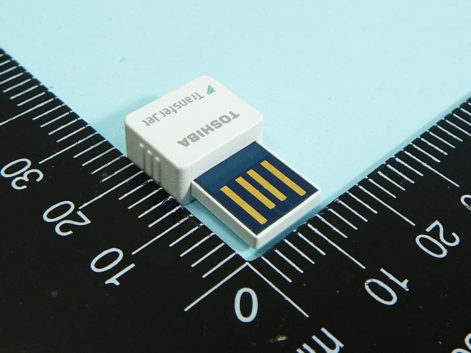
CJ6UPA5144TJ
Aug 07, 2014TransferJet USB Adapter
Equipment Class
JBP - Part 15 Class B Computing Device Peripheral
CJ6UPA5145TJ
Aug 07, 2014TransferJet MicroUSB Adapter
Equipment Class
UWB - Ultra Wideband Transmitter