CKEJHS-500Marine VHF
Japan Radio Co., Ltd.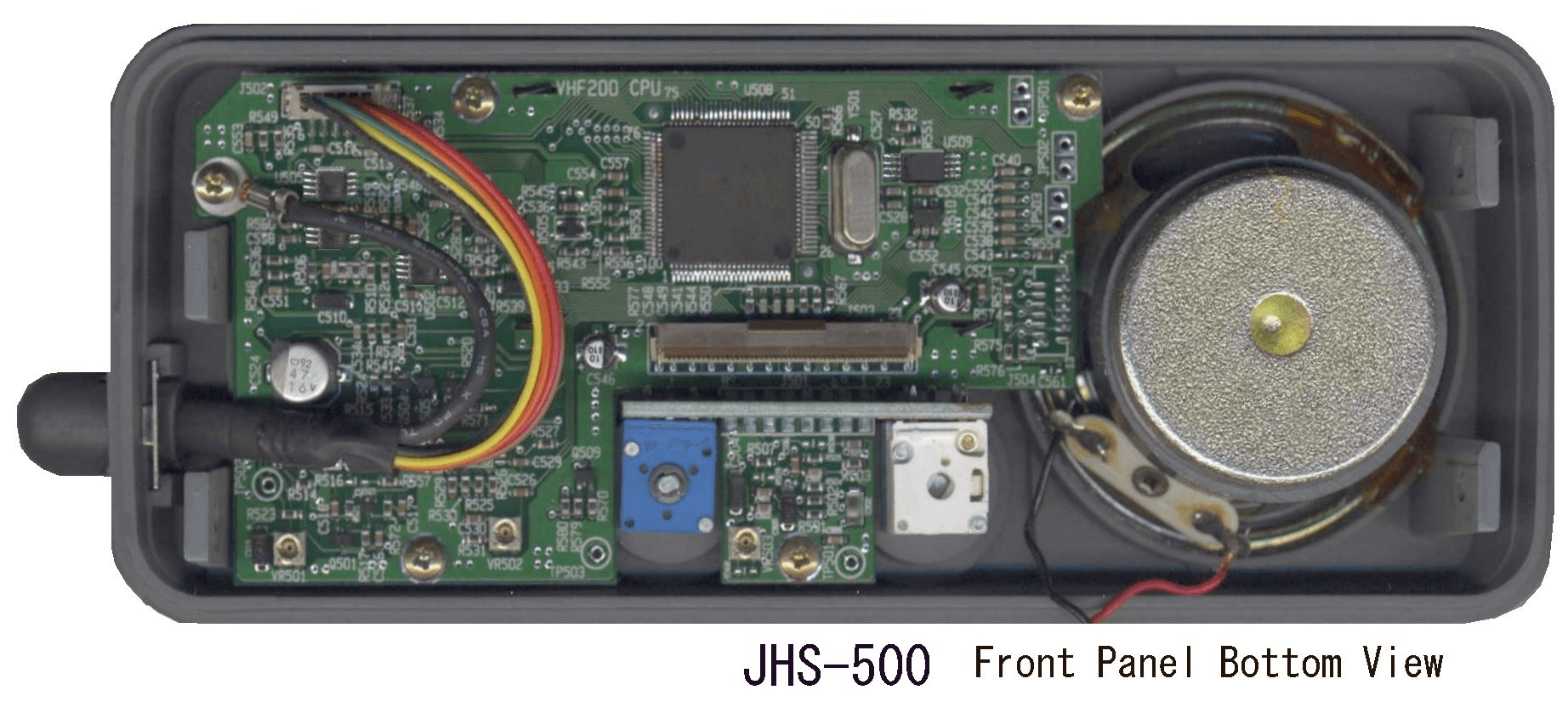
Click to zoom
Application Details
- Equipment Class
- GVH - Part 80 VHF Transmitter (GMDSS)
- Date of Grant
- Apr 09, 2001
- Application Purpose
- Original Equipment
- Date of Application
- Nov 12, 2000
- Equipment Note
- Marine VHF
- Frequency Range
- 156.02500000 - 157.42500000
- Company
- Japan Radio Co., Ltd.
- Country
- United States
Documents & Files
Document Text
Text extracted from the exhibit documents filed with the FCC. Open a document above to read the original.
Users Manual
MPE COMPLIANCE MPE compliance distance: 1.28 meters (4.2 feet) Users and other nearby individuals maintain 1.28 meters (4.2 feet) or more from a boat-mounted antenna during transmission. Compliance with the FCC's MPE limits in 47 CFR Section 1.1310, Table 1(b). * Maximum permissible exposure (MPE): The rms and peak electric and magnetic field strength, their squares, or the plane-wave equivalent power densities associated with these fields to which a person may be exposed without harmful effect and with an acceptable safety factor.
Users Manual
MPE COMPLIANCE Typical example of an Antenna MPE compliance distance 3dB gain 1/2-wave: 1.3 meters ( 4.2 feet) 6dB gain Collinear phased 5/8-wave: 2.0 meters ( 6.6 feet) 10dB gain Collinear array phased 1/2-wave: 3.2 meters (10.4 feet) Users and other nearby individuals maintain above distance or more from a boat-mounted antenna during transmission. Compliance with the FCC's MPE limits in 47 CFR Section 1.1310, Table 1(b). * Maximum permissible exposure (MPE): The rms and peak electric and magnetic field strength, their squares, or the plane-wave equivalent power densities associated with these fields to which a person may be exposed without harmful effect and with an acceptable safety factor.
Users Manual
MPE COMPLIANCE Typical example of an Antenna MPE compliance distance 3dBi gain 1/2-wave: 1.3 meters ( 4.2 feet) 6dBi gain Collinear phased 5/8-wave: 2.0 meters ( 6.6 feet) 10dBi gain Collinear array phased 1/2-wave: 3.2 meters (10.4 feet) Users and other nearby individuals maintain above distance or more from a boat-mounted antenna during transmission. Compliance with the FCC's MPE limits in 47 CFR Section 1.1310, Table 1(b). * Maximum permissible exposure (MPE): The rms and peak electric and magnetic field strength, their squares, or the plane-wave equivalent power densities associated with these fields to which a person may be exposed without harmful effect and with an acceptable safety factor.
Cover Letter(s)
1 General Characteristics General CharacteristicsGeneral Characteristics General Characteristics 1. Radio Compliance: FCC Part 2,15,80, DOC V. DSC (SC101-STD) 2. Number of Channels: All USA, International, Canadian and 10 Weather channels are included. 3. Input Voltage: 13.8 VDC+/-15% 4. Input Current: TX Less than 5.0A Max at 25 Watts Less than 1.5A Max at 1 Watt : RX (squelch) less than 250mA Max 5. Modulation Type: Frequency modulated 16K0F3E (G3E), G2B for DSC 6. Operating Temperature: -20°C ~ +55°C Transmitter Characteristics Transmitter CharacteristicsTransmitter Characteristics Transmitter Characteristics 1. Frequency Range: 156.025 to 157.425 MHz 2. Channel Spacing: 25KHz 3. RF Output Power: 25W / 1W, selectable into 50 ohms at 13.8VDC 4. Frequency Stability: +/-0.001% (-20°C ~ +55°C) 5. Frequency Deviation: +/-5KHz Max 6. Modulation AF Response: Within the limit of +1/-3 dB at 6dB/oct. frequency curve ( 300 ~ 3000Hz) reference ( 1000Hz) 7. Time-out-timer: 5 minutes +/-10% 8. Hum & Noise Level: Less than – 40dB below audio Less than 10% at 1KHz for +/-3KHz 9. Spurious & Harmonic Emission: Attenuated at least 43+10 Log Power ( below rated radiated carrier power) Receiver Characteristics Receiver CharacteristicsReceiver Characteristics Receiver Characteristics 1. Frequency Range: 15.025 to 163.275MHz in 25KHz increment 2. AF Output: 3 Watts ( Less than 10% at 1KHz) 3. AF Response: 6 dB/oct de-emphasis +1/-3dB from 300~3000Hz 4. Sensitivity: 0.3uV for 12 SINAD 5. Squelch Sens. Threshold: 0.15uV 6. Tight Squelch Sensitivity: 0.95uV 7. Adjacent Channel Selectivity: Better than 70dB 8. Spurious Image Rejection: Better than 70dB 9. Intermodulation: Better than 65dB 10. FM Hum and Noise: Less than – 40dB DSC DSCDSC DSC 1,Mark :1300Hz 2.Space :2100Hz 3. Frequency Stability: +/-10Hz (-20°C ~ +50°C) 4.Baulate :1200 bit/sec 5.Modulation Index :2+/-10% 6. DSC Format: RTCMSC101 2 Channel List Channel ListChannel List Channel List: VHF Marine Channel Frequencies : VHF Marine Channel Frequencies: VHF Marine Channel Frequencies : VHF Marine Channel Frequencies USA Version USA VersionUSA Version USA Version CHTXRX Type of Operation 01A156.050156.050Port operation &Com ’ l 05A156.250156.250Port operation 06156.300156.300Intership safety 07A156.350156.350Com ’ l 08156.400156.400Com ’ l 09156.450156.450Boater calling 10156.500156.500Com ’ l 11156.550156.550Com ’ l 12156.600156.600Port operation 13#156.650156.650Intership safety 14156.700156.700Port operation 15*156.750Environmental 16156.800156.800Emerg/calling 17**156.850156.850State controlled 18A156.900156.900Com ’ l 19A156.950156.950Com ’ l 20 157.700 161.600 Port operation 20A157.000157.000Port operation 21A##157.050157.050US Govern. only 22A157.100157.100Coast Guard 23A##157.150157.150US Govern. only 24157.200161.800Public corresp. 25157.250161.850Public corresp. 26157.300161.900Public corresp. 27157.350161.950Public corresp. 28157.400162.000Public corresp. *Transmitting is disabled. **1W only #1W initially. Can be switched to 25W. ##Not for use by the general public in U.S. waters. CHTXRX Type of Operation 63A156.175156.175Port operation &Com ’ l 65A156.275156.275Port operation 66A156.325156.325Port operation 67#156.375156.375Com ’ l 68156.425156.425Non com ’ l 69156.475156.475Non com ’ l 70156.525156.525DSC 71156.575156.575Non com ’ l 72156.625156.625Non com ’ l 73156.675156.675Port operation 74156.725156.725Port operation 77**156.875156.875Port operation 78A156.925156.925Non com ’ l 79A156.975156.975Com ’ l 80A157.025157.025Com ’ l 81A##157.075157.075US Govern. only 82A##157.125157.125US Govern. only 83A##157.175157.175US Govern. only 84157.225161.825Public corresp. 85157.275161.875Public corresp. 86157.325161.925Public corresp. 87157.375161.975Public corresp. 88 157.425 162.025 Public corresp 88A157.425157.425Com ’ l 3 Canadian Version Canadian VersionCanadian Version Canadian Version CHTXRXType of Operation 01156.050160.650Public corresp. 02156.100160.700Public corresp. 03156.150160.750Public corresp. O4A156.200156.200Coast Guard Com ’ l 05A156.250156.250Port operation 06156.300156.300Intership, Safety 07A156.350156.350Com ’ l, Intership 08156.400156.400Com ’ l, Intership 09156.450156.450Boater calling 10156.500156.500Com ’ l, Intership 11156.550156.550Com ’ l, Intership 12156.600156.600Port operation 13156.650156.650Intership safety 14156.700156.700Port operation 15156.750156.750Com ’ l,Non-com ’ l 16156.800156.800Emerg/calling 17156.850156.850State controlled 18A156.900156.900Com ’ l 19A156.950156.950Coast Guard 20157.000161.600Coast Guard 21A157.050157.050Coast Guard 22A157.100157.100Coast Guard 23157.150161.750Public corresp. 24157.200161.800Public corresp. 25157.250161.850Public corresp. 26157.300161.900Public corresp. 27157.350161.950Public corresp. 28157.400162.000Public corresp. 60156.025160.625Public corresp. 61A156.075156.075Coast Guard CHTXRXType of operation 65A156.275156.275Port operation 66A156.325156.325Port operation 67156.375156.375Com ’ l 68156.425156.425Non-com ’ l 69156.475156.475Com ’ l 70156.525156.525DSC 71156.575156.575Non-com ’ l 72156.625156.625Non-com ’ l 73156.675156.675Com ’ l 74156.725156.725Com ’ l 77156.875156.875Port operation 78A156.925156.925Non-com ’ l 79A156.975156.975Com ’ l 80A157.025157.025Com ’ l 81A157.075157.075Environmental 82A157.125157.125Coart Guard 83A157.175157.175Coast Guard 84157.225161.825Public corresp. 85157.275161.875Public corresp. 86157.325161.925Public corresp. 87157.375161.975Public corresp. 88157.425162.025Public corresp. Com ’ l 62A156.125156.125Coast Guard 64A156.225156.225Com ’ l 4 International Version International VersionInternational Version International Version CHTXRXType of Operation CHTXRXType of Operation 01156.050160.650Public corresp. 02156.100160.700Public corresp. 03156.15016.0750Public corresp. 04156.200160.800Public corresp. 05156.250160.850Public corresp. 06156.300156.300Intership safety 07156.350160.950Public correps. 08156.400156.400Com ’ l 09156.450156.450Boa…
Text truncated - open the document above for the full version.
ID Label/Location Info
ID Label / Location Information Unit:mm
Internal Photos
RF Unit Rear Side
Operational Description
1 VHF/FM RADIO TELEPHONE VHF/FM RADIO TELEPHONE VHF/FM RADIO TELEPHONE VHF/FM RADIO TELEPHONE JHS-500 JHS-500JHS-500 JHS-500 Technical Description Technical DescriptionTechnical Description Technical Description 1. RECEIVING CIRCUIT OPERATION: 1. RECEIVING CIRCUIT OPERATION:1. RECEIVING CIRCUIT OPERATION: 1. RECEIVING CIRCUIT OPERATION: 1.1 Antenna Switching Circuit: 1.1 Antenna Switching Circuit:1.1 Antenna Switching Circuit: 1.1 Antenna Switching Circuit: A signal received at the antenna terminal(J101) goes to the antenna switching circuit composed of pin diode D102 and D201 via the low pass filter. When a signal is received, D102 is ON, and D201 is OFF. 1.2 High Frequency Amplifier Circuit: 1.2 High Frequency Amplifier Circuit:1.2 High Frequency Amplifier Circuit: 1.2 High Frequency Amplifier Circuit: The high frequency signal from the antenna switching circuit is inputted to the transistor RF AMP(Q101) via D102. It is supplied to the 1st mixer AMP(Q102) after going through BPF which controls undesired signals. This 1st mixer is mixed with the receiving signal at the local oscillator(VCO: receiving signal + 46.025 MHz) and converted to 46.025 MHz 1st intermediate frequency. 1.3 1st Intermediate Frequency Amplifier Circuit 1.3 1st Intermediate Frequency Amplifier Circuit1.3 1st Intermediate Frequency Amplifier Circuit 1.3 1st Intermediate Frequency Amplifier Circuit The 1st intermediate frequency signal generated in the mixer circuit is amplified at the 1st IF AMP (U101) after undesired signals are removed by the crystal filter(Z101). 1.4 2nd Intermediate Frequency Amplifier Circuit: 1.4 2nd Intermediate Frequency Amplifier Circuit:1.4 2nd Intermediate Frequency Amplifier Circuit: 1.4 2nd Intermediate Frequency Amplifier Circuit: The 1st intermediate frequency signal is supplied to the 1st IF AMP(U101), which is composed of a local oscillating circuit, a mixer circuit, a limiter amplifier circuit, a remodulation circuit and a squelch circuit. The 1st intermediate frequency signal is converted to 455 kHz 2nd intermediate frequency signal after being mixed with the output signal which is composed in the local oscillating circuit in IC(U101) and the crystal oscillator (Y101: 45.570 MHz). The obtained signal is filtered by a ceramic filter (Z103,Z104) to discard the undesired signals, and then is amplified in the limiter amplifier circuit. The amplified 2nd intermediate frequency signal is re-modulated by the 2 re-modulation circuit composed of a circuit in IC(U101) and a ceramic discriminate element (Z102). Then it is outputted as a low frequency signal. This re-modulated low frequency signal obtains -6dB/oct response by passing through the de-emphasis circuit which is composed of LPE(U102), and goes into the low frequency amplifier. 1.5 Low Frequency Amplifier Circuit and Squelch Circuit: 1.5 Low Frequency Amplifier Circuit and Squelch Circuit:1.5 Low Frequency Amplifier Circuit and Squelch Circuit: 1.5 Low Frequency Amplifier Circuit and Squelch Circuit: The re-modulated low frequency signal is amplified by AMP(U403). Its volume can be controlled by the volume(VR501). Busy signal, generated in the squelch circuit in IC(U101), is processed to mute signal in CPU(U508). This signal switches the low frequency signal on and off by driving the transistor switch(Q506). WX Alert Detection: If 1050 Hz tone signal is contained in the receiving signals, it is detected by the tone detector(U503), processed in CPU, and outputted as an alert signal from CPU. 2. TRANSMITTING CIRCUIT OPERATION 2. TRANSMITTING CIRCUIT OPERATION2. TRANSMITTING CIRCUIT OPERATION 2. TRANSMITTING CIRCUIT OPERATION 2.1 Exciter Amplifier and Power Amplifier Circuit: 2.1 Exciter Amplifier and Power Amplifier Circuit:2.1 Exciter Amplifier and Power Amplifier Circuit: 2.1 Exciter Amplifier and Power Amplifier Circuit: When the PTT switch of the microphone is pressed, the mode turns to trans- mitting, and frequency of PLL is set up to transmitting frequency. At the same time, transistors of the transmitting/receiving shift circuits(Q406,Q409 and Q411) are driven to operate VCO(Q301). The high frequency signal of VCO (Q301) is amplified by the Buffer Amplifier(Q303) and the Exciter Amplifiers(Q201, Q202), and supplied to Power Module(U201). It is power- amplified to the maximum output of 25W in the Power Module(U201), and outputted from the Antenna Terminal(J101) via the Antenna Switching Circuit diodes(D102,D201). 2.2 FM Modulation Circuit: 2.2 FM Modulation Circuit:2.2 FM Modulation Circuit: 2.2 FM Modulation Circuit: Voice signal from the microphone is amplified by the amplifier(U401a), and gets pre-emphasis response of 6 dB/oct in the range of 300 Hz ~3 kHz. The amplitude of this signal is limited by the limiter circuit(D401), and its high frequency distortion is eliminated by LPFs(U402a,U402b). Then it is inputted to TX,VCO circuit as a 3 modulation signal. This modulation signal is supplied to a variable capacity diode (D303) attached to VCO circuit(Q301), and FM-modulated. 2.3 APC(Automatic Power Control): 2.3 APC(Automatic Power Control):2.3 APC(Automatic Power Control): 2.3 APC(Automatic Power Control): A part of the power amplified by power module(U201) is converted to direct current signal voltage by diode (D202). This direct current voltage is amplified by direct current amplifiers(Q203,Q204,Q205), and controls power source voltage of the power module(U201). Output power is switched between 1w and 25w with 1w/25w switch (Q207) which is controlled by the direct current amplifier. VR201 and VR202 are used for fine tuning of 1w and 25w, respectively. Then the output power is outputted through the low pass filter circuit (L201,L202,L203,L212,C201,C202,C203,C204 and C244) which suppress spurious emissions. 3. PLL 3. PLL 3. PLL 3. PLL SYNTHESIZER SYNTHESIZERSYNTHESIZER SYNTHESIZER PLL IC(U301) oscillates 12.8 MHz frequency by crystal oscillator(Y301). This 12.8 MHz frequency is divided into 1/512 by the divider inside the IC…
Text truncated - open the document above for the full version.
Parts List/Tune Up Info
1 VHF/FM RADIO VHF/FM RADIO VHF/FM RADIO VHF/FM RADIO TELEPHONE TELEPHONE TELEPHONE TELEPHONE JHS-500 JHS-500JHS-500 JHS-500 Alignment Procedure Alignment ProcedureAlignment Procedure Alignment Procedure This section describes the alignment procedure for the radio. Please refer to the alignment location diagram. 1. Test Equipment: The following test equipment is recommended for radio alignment. * Communication Monitor (HP8920B or equivalent) * DC Voltmeter (>1 megohms input impedance) * DC Power Supply ( 10 to 20 volts at 10 amp) * RF Coaxial Cable * Power Cable 2. Initial Setup NOTE: > Connect DC power cable to radio and set voltage on power supply for 13.8 volts. > Connect radio to Communication Monitor. > Turn on radio and note 16 channel on LCD segments light. VCO > Set the power supply voltage to 13.8 V > Select radio channel 16 > Use high impedance prove to measure the VCO control voltage at TP1 > Align the trimmer capacitor C317 for RX VCO control voltage : 1.6V > Key the radio under low power mode > Align the trimmer capacitor C318 for TX VCO control voltage : 1.8V 2 Reference OSC > Set the power supply voltage to 13.8V > Select radio channel 16 and key the radio under low power mode > Align the trimmer capacitor C337 to obtain 156.800+/-100Hz at the room temperature RF Output Power > Set the power supply voltage to 13.8V > Select radio channel 16 and key the radio under low power mode > Align VR201 to obtain 0.9W RF output power > Set the radio for high power mode > Align VR202 to obtain 24W RF output power Transmitter Modulation > Set the power supply voltage to 13.8V > Select radio channel 16 and key the radio under low power mode > Apply a 1KHz tone at 140 mV input level to the transmitter audio input (J503) > Adjust modulation control VR401 to obtain the maximum deviation 4.5KHz Note: HP8920B : <20Hz HPF,15k LPF, De-emph. off,Peak +/-Max RX Tone Decoder > Set the power supply voltage to 13.8V > Press “ WX ” key and select radio channel WX1 > Provide RF signal : 162.550 MHz, -113dBm modulated with 1050Hz tone at the standard deviation (3.0 kHz) > Rotate the volume control VR503 and note the location that “ ALT ” flashes on the LCD display > Rotate further the VR501 and note the location that “ ALT ” turned off Set the VR503 between them 3 1. RF PCB Alignment Location 2. LOGIC PCB Alignment Location VR401C337C317C318VR201VR202 VR501VR502VR503 TP1 4 PC Board VIEW 1) RF Unit Side A 2) RF Unit Side B 5 3) LOGIC Unit Side A 4) LOGIC Unit Side B
Parts List/Tune Up Info
VHF/FM RADIO TELEPHONE VHF/FM RADIO TELEPHONEVHF/FM RADIO TELEPHONE VHF/FM RADIO TELEPHONE JHS-500 JHS-500JHS-500 JHS-500 List of RF Circuit Components: List of RF Circuit Components:List of RF Circuit Components: List of RF Circuit Components: Part No. NameCharacteristicsVendor D102M1809RF Switching PIN Diode 10W, SMTMITSUBISHI D201M1809RF Switching PIN Diode 10W, SMTMITSUBISHI D2021SS383(TE85L)Schottky Barrier Diode DualTOSHIBA D2031SS371 (TPH3)Band Switch DiodeTOSHIBA D3011SV281 (TPH3)Varactor Diode, rs=.28, c1v/c4v=2.0TOSHIBA D3021SV281 (TPH3)Varactor Diode, rs=.28, c1v/c4v=2.0TOSHIBA D3031SV214 (TPH3)Diode 1SV214TOSHIBA D401DAP202KTSwitching Diode 1.2V@100mA SMD3ROHM D402U2FWJ44N(TE12R)Schottky Barrier Diode .37V@2A, I-FLATTOSHIBA D40302CZ13Y(TE85R)Zener Diode 13VTOSHIBA D404DAP202KTSwitching Diode 1.2V@100mA SMD3ROHM Q1012SC5086-Y(TE85L)RE Transistor LNATOSHIBA Q102GN2012MMIC Mixer Dual gateMATSUSHITA Q2012SC5086-Y(TE85L)RF Transistor LNATOSHIBA Q2022SC3357TRF TR Power mini moldNEC Q2032SB1184TLRGeneral Mid. Tr,3A, 15WROHM Q2042SC4116-GR(TE85L) General TransistorTOSHIBA Q2052SC4116-GR(TE85L) General TransistorTOSHIBA Q206DTC114EEDigital Transistor 50mA (10K 10K) ROHM Q207DTC114EEDigital Transistor 50mA (10K 10K) ROHM Q209DTA114EEDigital Transistor 50mA (10K 10K) ROHM Q210DTC114EEDigital Transistor 50mA (10K 10K) ROHM Q3012SK508-T1BFET for VCONEC Q3022SK508-T1BFET for VCONEC Q3032SC5086-Y(TE85L)RF Transistor LNATOSHIBA Q3042SC4116-GR(TE85L) General TransistorTOSHIBA Q3052SC5086-Y(TE85L)RF Transistor LNATOSHIBA Q4012SD2396General Mid. Tr, 3A T0-220 LEADROHM Q402FMC1ADigital TR Power management 100mAROHM Q403FMC1ADigital TR Power management 100mAROHM Q406DTC114EEDigital Transistor 50mA (10k 10k)ROHM Part No. NameCharacteristicsVendor Q407FMC1ADigital TR Power management 100mAROHM Q408DTC114EEDigital Transistor 50mA (10k 10k)ROHM Q409DTC114EEDigital Transistor 50mA (10k 10k)ROHM Q410DTA114EEDigital Transistor 50mA (10k 10k)ROHM Q411DTA114EEDigital Transistor 50mA (10k 10k)ROHM Q412 2SK209-BL J-FET SSM TOSHIBA Q413 DTC1314TUDigital Transistor 50mA (10k)ROHM U101TA31137FN(EL)IF IC ( .65 SSOP)TOSHIBA U102NJM2100MOP AMP DMP8=SOP8(6.8)JRC U201S-AV6PA Module 25WTOSHIBA U301TB31202FN(ER)Synthesizer IC dualTOSHIBA U401NJM062MOP AMPJRC U402NJM2100MOP AMP DMP8=SOP8(6.8)JRC U403BA5417Audio PA stereo 5W 12V 3ohm HSIP-15ROHM U404TA7805F(TE16L)Series Regulator 5V 1A 2VTOSHIBA U405 TLP181-GR OPTO ISOLATOR TOSHIBA List of Logic Circuit Components List of Logic Circuit ComponentsList of Logic Circuit Components List of Logic Circuit Components : Part No. NameCharacteristicsVendor D501AY1101F-TRCHIP LED Side ViewSTANLEY D502AY1101F-TRCHIP LED Side ViewSTANLEY D503AY1101F-TRCHIP LED Side ViewSTANLEY D504AY1101F-TRCHIP LED Side ViewSTANLEY D505 DA227Switching Diode 80V@100mA ROHM D506AY1101W-TRCHIP LED Top ViewSTANLEY D507AY1101W-TRCHIP LED Top ViewSTANLEY D508AY1101W-TRCHIP LED Top ViewSTANLEY D509AY1101W-TRCHIP LED Top ViewSTANLEY D510AY1101W-TRCHIP LED Top ViewSTANLEY Q5012SC4116-GR(TE85L) General TransistorTOSHIBA Q503 2SK2035(TE85R)S-MOS FET SSMTOSHIBA Q504DTC114EEDigital Transistor 50mA (10k 10k)ROHM Q505DTC1314TUDigital Transistor 50mA (10k)ROHM Q506DTC114EEDigital Transistor 50mA (10k 10k)ROHM Q507DTC114EEDigital Transistor 50mA (10k 10k)ROHM Q5082SC4116-GR(TE85L) General TransistorTOSHIBA Q5092SC4116-GR(TE85L) General TransistorTOSHIBA U501NJM2211M FSK-Demodulater JRC U502TC7W53FU Dual Multiplexer TOSHIBA U503 BA1604F-E2PLL Tone DecoderROHM U504TC3W03FU C ounter / Oscillator TOSHIBA U505TC7W53FU Dual Multiplexer TOSHIBA U506TC7W53FU Dual Multiplexer TOSHIBA U508 M38257E8GP CPU QFP 0.5 100pin MITSUBIIHI U509BR93LC56FV EEPRM2k bitROHM U510 RN5VL45CVoltage Detector 4.5VRICOH
RF Exposure Info
1 Test Setup HP8920B HP8657A ANRITSU HP8560E RF Communication Signal Signal Spectrum Test Set Generator Generator Analyzer 3 Signal Pad FUJISOKU FAT-550A 20 dB Attenuator FUJIKURA RG-55U+ M-N coaxial cable(1m)HIROSE –1120 20 dB Attenuator SETKENWOOD PD 18-20A JHS-500DC Power Supply 70ch:156.525MHz Occupied Bandwidth (DSC mode) 2-3. Maxmum Permissible Exposure Test Frequency : CH16(156.8MHz) Transmitter Output : 25W Antenna : Half-wave dipole antenna Frequency (MHz) Electric field Strength (V/m) Magnetic field Strength (A/m) Power density (mW/cm 2 ) Averaging Time (min) Needed Separation Distance (m) 156.827.5 *Note 0.073 *Note 0.2 *Note 30 *Note 1.28 *Note : Limits for MPE in CFR47 Sec tion1.1310 & Table 1(b) 17
Test Report
1 Test Setup HP8920B HP8657A ANRITSU HP8560E RF Communication Signal Signal Spectrum Test Set Generator Generator Analyzer 3 Signal Pad FUJISOKU FAT-550A 20 dB Attenuator FUJIKURA RG-55U+ M-N coaxial cable(1m)HIROSE –1120 20 dB Attenuator SETKENWOOD PD 18-20A JHS-500DC Power Supply 70ch:156.525MHz Occupied Bandwidth (DSC mode) 2-3. Maximum Permissible Exposure Test Frequency:CH16(156.8MHz) Transmitter Output:25W Electric field Strength: 27.5 V/m*Note Magnetic field Strength: 0.073 A/m*Note Power Density:0.2 mW/cm 2 *Note Averaging Time:30min*Note *Note: Limits for MPE in CFR47 Section1.1310 & Table 1(b) Needed Separation Distance Typical example of Antenna Antenna Gain (dB) (m)(ft.) Half-wave dipole2.151.34.2 Collinear phased 5/8-wave62.06.6 Collinear array phased 1/2-wave 103.210.4 1 7
Test Report
1 Test Setup HP8920B HP8657A ANRITSU HP8560E RF Communication Signal Signal Spectrum Test Set Generator Generator Analyzer 3 Signal Pad FUJISOKU FAT-550A 20 dB Attenuator FUJIKURA RG-55U+ M-N coaxial cable(1m)HIROSE –1120 20 dB Attenuator SETKENWOOD PD 18-20A JHS-500DC Power Supply 70ch:156.525MHz Occupied Bandwidth (DSC mode) 2-3. Maximum Permissible Exposure Test Frequency: CH16(156.8MHz) Transmitter Output: 25W Electric field Strength: 27.5 V/m *Note Magnetic field Strength: 0.073 A/m *Note Power Density: 0.2 mW/cm 2 *Note Averaging Time: 30min *Note *Note: Limits for MPE in CFR47 Section1.1310 & Table 1(b) Needed Separation Distance Typical example of Antenna Antenna Gain (dBi) (m) (ft.) Half-wave dipole 2.15 1.3 4.2 Collinear phased 5/8-wave 6 2.0 6.6 Collinear array phased 1/2-wave 10 3.2 10.4
Contact Information
Applicant
Yuji Kinoshita(General Manager)
Technical Contact
Japan Radio Co.,Ltd. Seattle Branch OfficeDennis Sethe
[email protected]206-654-6544
1011 SW Klickitat Way · Seattle, Washington · United States
Non-Technical Contact
Japan Radio Co.,Ltd. Seattle Branch OfficeShunichi Hasama
[email protected]206-654-5644
Test Firm
Japan Radio Co., Ltd.Mitsuru Okamoto
Technical Specifications
| # | Rule Parts | Frequency Range | Power Output | Emission | Tolerance |
|---|---|---|---|---|---|
| 2 | 80.1101(c)(2) | 156.025 MHz - 157.425 MHz | 1 W | 16K0G3E | 0.001 % |
Other Applications from Japan Radio Co., Ltd.
CKENTG1014
May 09, 20235G Radio Unit
Equipment Class
CBD - Citizens Band Category A and B Devices
CKENKE2632
Oct 21, 2015Solid State S-Band Marine Radar
Equipment Class
MRD - Marine Radar
CKENJJ-200
Jan 22, 2015Handy Search
Equipment Class
UWB - Ultra Wideband Transmitter
CKEJRN-130K
Oct 21, 20143G/GSM IT Controller
Equipment Class
PCB - PCS Licensed Transmitter
CKENKE1066
Feb 04, 2014MARINE RADAR
Equipment Class
MRD - Marine Radar