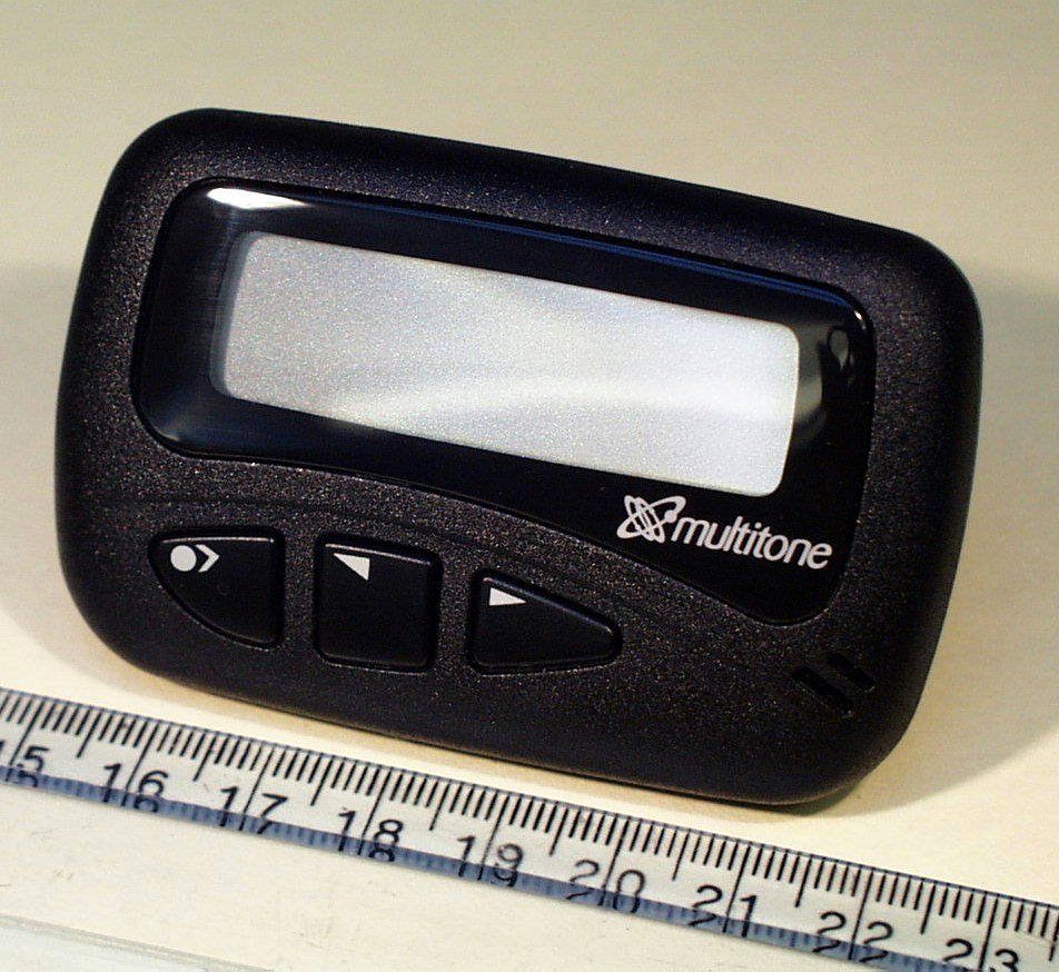
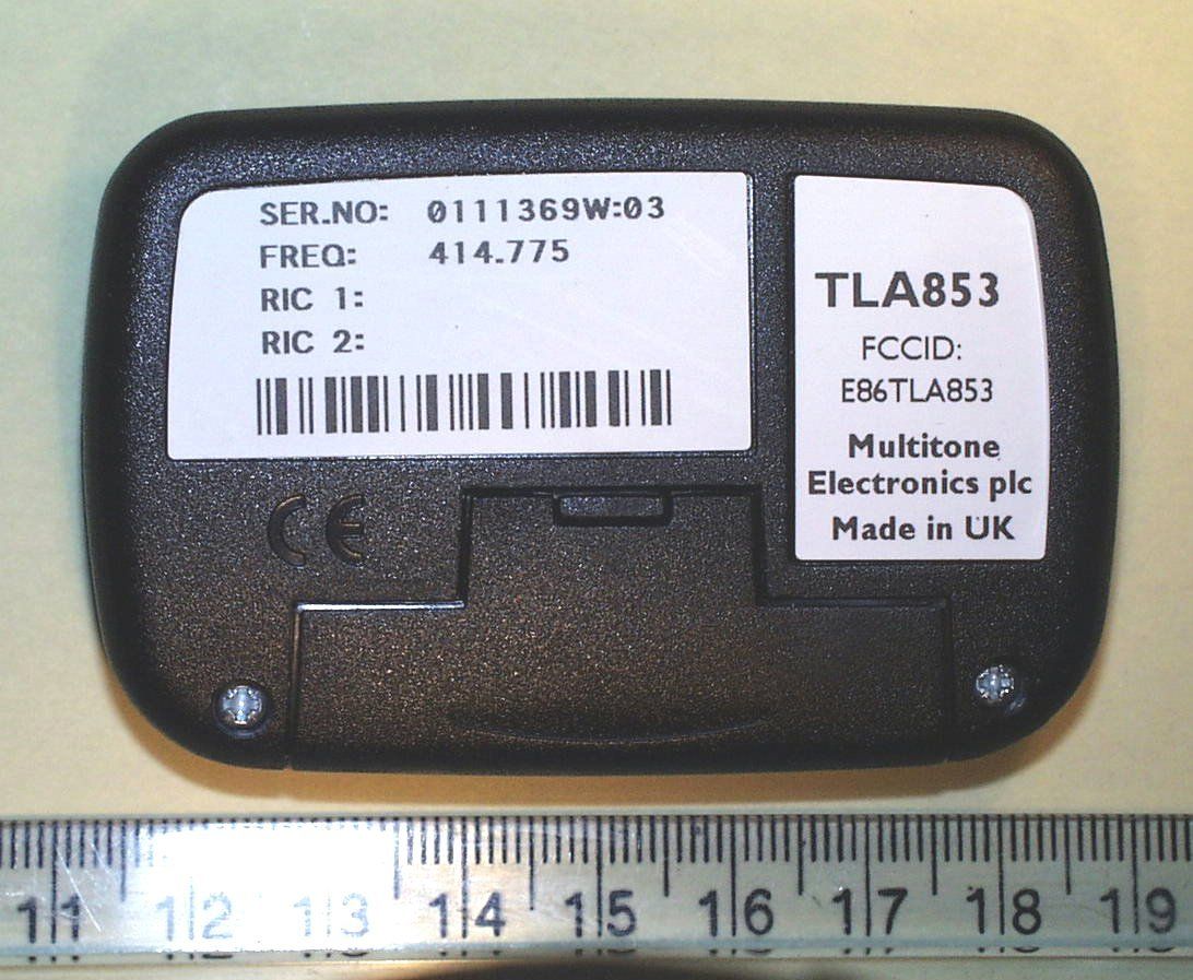
E86TLA853-FPager Receiver
Multitone Electronics PLC
Click to zoom
Application Details
- Equipment Class
- CXX - Communications Rcvr for use w/ licensed Tx and CBs
- Date of Grant
- Jan 12, 2003
- Application Purpose
- Original Equipment
- Date of Application
- Jan 12, 2003
- Equipment Note
- Pager Receiver
- Frequency Range
- 406.00000000 - 412.00000000
- Company
- Multitone Electronics PLC
- Country
- United Kingdom
Documents & Files
Document Text
Text extracted from the exhibit documents filed with the FCC. Open a document above to read the original.
Users Manual
Contents Introduction and Getting Started .............. 1 Switching the Pager On ............................ 1 Status and Operating Symbols ................ 2 Setting the Time and Date ........................ 4 Setting the Pager Alarm ........................... 6 Selecting the Pager Alert ......................... 8 Receiving a Message ............................. 10 Reviewing Stored Messages .................. 11 Archiving Messages ............................... 12 Reviewing Archived Messages .............. 13 Deleting Messages ................................. 13 Deleting All Messages ............................ 14 Timed Off ................................................ 14 Reviewing Information Service Messages ............................................. 16 Caring for your Pager ............................. 17 Fault-Finding ........................................... 17 (i) Releasing the Pager from the Holster Press on the bottom tag with your finger and slide the pager upward. (ii)1 Introduction and Getting Started Congratulations on selecting the TLA 850 alphanumeric pager from Multitone. Your pager has all the features you expect of a top class product yet it retains simplicity of operation through the superbly designed user interface and icon menu selection. This guide will describe the operation of the product and ensure that you receive the full benefits of paging with the TLA 850. On the back of your pager you will find the battery cover. Press down on the centre tab while sliding the battery cover outwards to remove. Insert the battery into the spring end first so that the + symbol on the battery is aligned with the moulded + symbol in the battery compartment. Carefully slide the cover back into position. Switching the Pager On To turn the pager on press and hold the •> button for one second. A short alert will 2 14:24 23.03.98 sound and the pre-programmed switch-on message will be displayed. After one second the time and date will be shown. This is the standby screen: Standby Screen Status and Operating Symbols The standby screen shows the current time and date. It also shows if there are unread messages, whether audible or vibrate alert is selected and, if appropriate, gives low battery and out-of-range warnings by displaying the following symbols: Status Symbols 14:26 23.03.98 3 From the standby screen press •> to enter the pager options screen. The following symbols are displayed: Pager Option Screen Unread MessagesLow Battery Audible AlertOut-of-Range VibrateMemory Full The status symbols are as follows: Archive Alert Section Time Setting and Timed Off Setup Off Alarm Function Backlight Delete All Messages 4 To turn the pager off press •> to show the pager options screen and then press < or > several times until the symbol is flashing. Press •> and the display will show the symbol plus a flashing ?. Press •> again to turn the pager off. Setting the Time and Date The standby screen will normally show the time and date. To set the current time and date press •> once to display the pager options and then press < or > several times until the symbol flashes. Press •> to display the time function edit screen. Time Function Screen The clock symbol will flash. To set the clock press •> and the clock symbol will 5 appear with 12 or 24 hour mode indicated. The hour will flash and the correct value may be selected by pressing either < or >. Once the hour is correct press •> and the tens of minutes will flash. Press < or > until the correct number is shown and then press •>. Press < or > until the correct number is shown and then press •> to set the minutes. The date is set with the same method. 5:27 pm 23.03.98 12 5:27 pm 23.03.98 12 5:29 pm 23.03.98 12 6 Once the display shows the correct time and date the 12 or 24 hour mode can be selected by pressing the < or > buttons to change as required. Press and hold •> for one second to return the pager to the standby screen. Setting the Pager Alarm The pager has a daily alarm feature and it may be set by pressing the •> to show the pager options and then selecting the symbol using the < or > buttons. Press the •> to display the alarm options screen. To turn the alarm on press < or > until the symbol shows and the time that the alarm is set to sound is displayed. 17:27 pm 23.03.98 24 7 To turn the alarm off press < or > until the symbol shows and the alarm time is turned off. To change the alarm time press •> and the hour will flash. Press < or > to change the numbers and when the correct value is set press •> and the tens of minutes will flash. Press < or > to change the numbers and when the correct value is shown press •>. Press < or > until the minutes display is correct and then press •> for one second to return to the standby screen. 07:00 8 The display will show the symbol indicating that the alarm is set. When the alarm time is reached the standby screen will show the symbol flashing and the alert will sound for eight seconds. Pressing any button within the eight second period will stop the alert. Selecting the Pager Alert To set the alert on the pager press •> to show the pager options and then press < or > several times until the symbol is flashing. Press •> to display the alert options screen which allows you to select the type of alert that the pager produces when a call is received. The pager has nine possible alert 9 settings. These are numbered 0 for No alert, 1 for Vibrate alert and 2 to 8 for the seven audible alerts. Press < or > to change the alert and the pager gives you a sample of the alert. To stop the alert press any button. If the vibrate alert is required then press the < or > until the symbol is displayed and the pager will vibrate for one second. The pager will now vibrate discreetly when a call is received. Once the desired alert has been selected press •> for one second to return to the standby screen. In the standby screen the pager will now show the symbol if the audible alert has been selected. T…
Text truncated - open the document above for the full version.
Users Manual
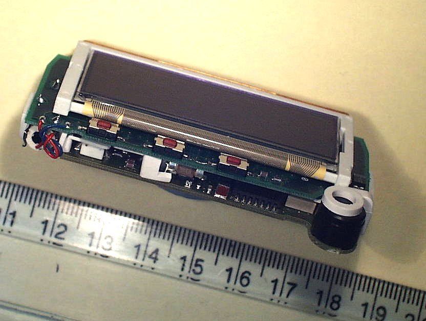
TLA 852/853 • Small and convenient • Two-line display • 32 Memories • Personal and Group RICs • 8 Special Services (mailboxes) • Vibrate as standard • Runs on one AAA battery • Alarm clock • Delete All feature • Battery saver Two-Line Alphanumeric Pagers The new Multitone™ TLA 850 range is small, attractive and easy to use. Two-line display The large LCD shows two rows, each of 14 easily visible alphanumeric characters. New messages appear instantly on the display - their time stamp appears last. Using the TLA In standby mode the display shows time, date and status information. Simply press the right button to view stored messages, the middle button to access the archive (Special Services instead if enabled) or the left button to set your user options. These include choosing the alert type, setting the clock, selecting the battery saver times and deleting all messages - all done via easily understood icons: Archive Alarm Backlight Battery Saver Delete All AlertOff Multitone Electronics plc Head Office Multitone House Beggarwood Lane Kempshott Hill Basingstoke Hampshire RG23 7LL Tel: +44 (0) 1256 320292 Fax: +44 (0) 1256 462643 E-Mail: [email protected] Web Site: www.multitone.com Northern/Scottish Office Unit 33, Geddes House Kirkton North Livingston West Lothian EH54 6GU Tel: 01506 418198 Fax: 01506 411711 Multiton Elektronik GmbH Dusseldorf, GERMANY Multiton Elektronik GmbH Vienna, AUSTRIA PL0319/1 The Multitone policy is one of continual improvement, so equipment may vary in detail from the description and specification in this publication. © Multitone Electronics plc 1998 Designed and manufactured in accordance with Quality System ISO 9000. Certificate Nos. FM20122 and Q10379. SPECIFICATION RADIO PERFORMANCETLA 852 (VHF)TLA 853 (UHF) Frequency range137.5-174MHz439-470MHz Channel spacing25kHz25kHz Sensitivity (typical for 40 character message) Best position 512 Baud5μV/m5μV/m 1200 Baud7μV/m8μV/m 2400 Baud10μV/m12μV/m 8 Position average 512 Baud8μV/m9μV/m 1200 Baud11μV/m12μV/m 2400 Baud15μV/m17μV/m Intermodulation rejection60dB55dB Adjacent channel sensitivity70dB60dB Spurious response60dB60dB Image response65dB50dB Spurious emission <1GHz (max.) 2nW2nW DISPLAYSTN LCD IlluminationBulb backlighting to LCD Display area48mm x 13.5mm Capacity2 Rows of 14 characters Time and date12 or 24 Hour selectable Alarm time functionSingle alarm, daily alert Also battery saving “Timed Off” function ALERTS Audible (typical)76dB SPL @ 30cm Alert tones7 Plus vibrate and silent Max. number of messages32 Personal messages Max. number of characters per message1024 Message archive capacity6 Archive locations Total Number of RICs4 Personal Paging RICs2 Information Service RICs2 Permitting a total of 8 services Message time stampStandard LanguagesCountry specific ASCII characters AccessoriesHolster, lanyard, battery and guide Code formatCCIR RPC No. 1 (POCSAG) CE Approved ENVIRONMENTAL Operating temperature-10°C to +55°C Storage temperature-20°C to +70°C PHYSICAL Width x Height75mm x 49mm Thickness16.5mm Volume60cm 3 Weight (including AAA battery)65g
Block Diagram
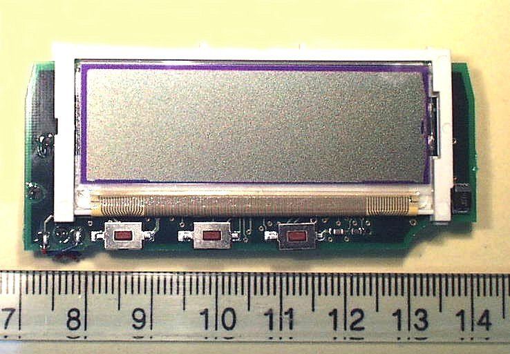
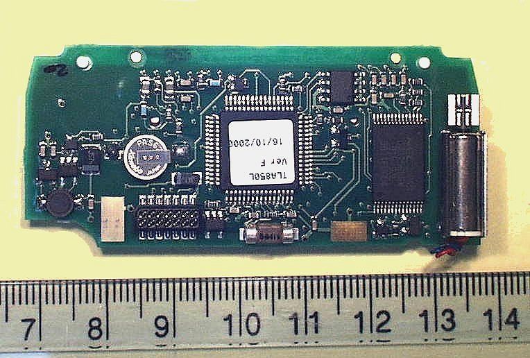
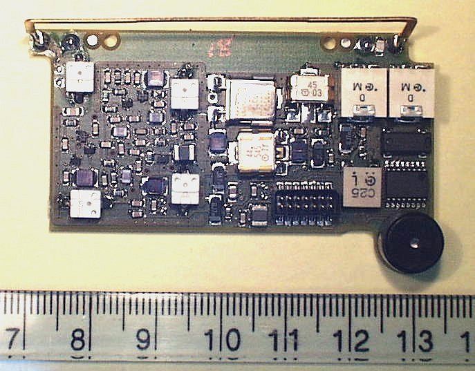
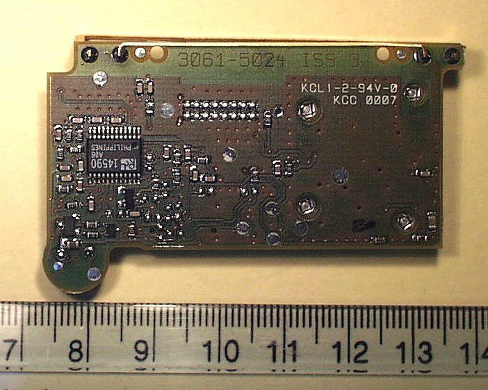
RADIO BOARDDECODER BOARD AUDIBLE ALERT BATTERY CONVERSION RECEIVER DUAL DECODER POCSAG CONVERTER SUPPLY VOLTAGE BACK-UP LIQUID EEPROM CRYSTAL DISPLAY MODULE SRAM M DISPLAY LAMP VIBRATE MOTOR MICRO- PROCESSOR B+ V DD PL401 SK1 DATA TAG11121-1 DATA ADDR CONTROL B+ V DD GND B+ VDD GND CHG RXEN LOBAT PROG 1 Figure 1: TLA 853 Block Diagram Multitone TLA 853 - Technical Description 1CIRCUIT SUMMARY The TLA 853 message receiver consists of two Printed Circuit Board (PCB) assemblies contained in a plastic case. The case is constructed in two main parts, the case front and the case back. A cover on the back of the TLA 853 provides access to the battery compartment. The two boards in the case are: a)The Radio Board which has the Dual Conversion Receiver, the POCSAG Decoder, the 1 Volt regulator and the audio alert output circuit and transducer. b)The Decoder Board which has the microprocessor, the EPROM, the SRAM, the Liquid Crystal Display Module, the LCD illumination lamp, the vibrate motor and the primary and backup power supplies. The block diagram of the functional areas of the TLA 853 is shown in Figure 1. 2 The RF signal enters the aerial and is fed to the dual conversion superheterodyne receiver. The signal is demodulated from RF to AF, converted to digital format and is then fed to the decoder. This results in the received data activating the memory, display and the selected audible alert or vibrate alert. To prolong the life of the battery, the receiver operates with battery economy mode. When the unit is in standby mode, the receiver is powered up at regular intervals (equivalent to once per batch) to allow the POCSAG decoder to search for pre-amble. While the unit is receiving preamble on its allocated channel, the receiver remains powered up. This allows the POCSAG decoder to search for a SYNC word. When the SYNC word is found, ‘batch lock’ is acheived. In batch lock the receiver is only powered up during the allocated frame to allow the POCSAG decoder to search for its address. If the address is found, the receiver stays ON for the duration of the message. RF AMPLIFIER TR403 MIXER AE401 AE402 2nd OSC. MIXER 455kHz TR401, TR402 45 MHz CER FL402 IC401 MIXER, IF AMP & DET. TR410, TR414 1st OSC. FL401 IF AMP XL402 XL401 TAG11120-1 455kHz CER FL403 CV404 AGC CONTROL TR407 TP403 IMAGE FILTER GNDGND CV407 CV406 CV405 TP405 RSSI DET DELAY FL404 DATA TO DECODER TP401 SINAD FSK COMP. FILTER QUICK CHARGE AMP PHASE 1V REG TR406 1V SUPPLY 1V TP402 INT. REF. RXEN LOWB 3 Figure 2: Receiver Block Diagram 2DUAL CONVERSION RECEIVER The incoming RF signal is received by the aerial AE401/AE402 which is tuned by CV404. Capacitors C401 and C441 provide matching to RF amplifier TR401, TR402. The amplifier, typically, yields a low noise gain of 10dB. R401, R402 and TR407 provide DC negative feedback. 4 Output from the RF amplifier passes through an image filter which provides these functions: a)Attenuation of the first image frequency. b)Attenuation of signals outside the required band. c)Matches the output impedance of the RF amplifier to the input impedance of the mixer stage. C406, L401 and CV407 form a parallel tuned circuit with the resonant frequency adjusted for minimum loss at the frequency of operation. C428, CV406 and L407 also form a parallel tuned circuit adjusted for minimum loss at the frequency of operation. In addition, C428 and L407 form a series resonant circuit with the resonant frequency close to the first image frequency. This gives approximately 40dB of attenuation at the image frequency. The local oscillator comprises transistor TR410, crystal XL402 and associated components. Frequency adjustment is by CV405. The local oscillator frequency is calculated as follows: carrier frequency - 45MHz fx = 3 where fx is the crystal frequency in MHz. The collector of TR410 is tuned to the third harmonic of XL402 by L411 and C459. The circuit provides the correct Local Oscillator frequency and reduces the level of 2nd, 4th and higher harmonics. The two tuned circuits, L413, C463 and L415, C464 give further filtering of unwanted harmonics. The mixer circuit, TR403 and associated components, receives the output of the image filter. This is mixed with the local oscillator output to produce a 45MHz product which is selected by the resonant circuit L406, C451. The 45MHz output passes through a monolithic crystal filter, FL401, which has a bandwidth of ±7.5 kHz at the -3 dB points. The output from FL401 is fed to IC401 pin 24. IC401 is a combined mixer/local oscillator/IF/detector. The second oscillator runs at 44.545MHz and, with the exception of XL401 and its associated components, is built into the IC. As the second oscillator is not trimmed, small frequency errors are absorbed when tuning the first local oscillator. The input at pin 24 is applied to the internal second mixer, and is mixed with the second oscillator output to produce a 455 kHz 2nd IF signal at pin 3. The IF signal then passes through two ceramic filters FL402 and FL403 which remove unwanted mixer products and provide further selectivity. The output from FL403 is split: one output connects through C450 to pin 6 of IC401 and the IF amplifier; the other connects to the Received Signal Strength Indicator (RSSI) circuit in IC401 through C419, R407 and pin 5. 5 Due to the characteristics of filters FL401, FL402 and FL403, the signal at the input to the IF amplifier has amplitude modulation (AM). The AM must be removed before the signal reaches the detector stage. This is performed by the IF amplifier in IC401 which has very high gain and is designed to limit the amplitude of the signal to remove the AM component and give a ‘square’ output. C479 and C480 provide de-coupling for the IF amplifier. The output from the IF amplifier passes to the detector in IC401. This circuit is a Quadrature Demodulator which has two inputs. One input connects directly to the IF amplifier, the other receives the signal from the IF amplifier through a phase del…
Text truncated - open the document above for the full version.
Operational Description
RADIO BOARDDECODER BOARD AUDIBLE ALERT BATTERY CONVERSION RECEIVER DUAL DECODER POCSAG CONVERTER SUPPLY VOLTAGE BACK-UP LIQUID EEPROM CRYSTAL DISPLAY MODULE SRAM M DISPLAY LAMP VIBRATE MOTOR MICRO- PROCESSOR B+ V DD PL401 SK1 DATA TAG11121-1 DATA ADDR CONTROL B+ V DD GND B+ VDD GND CHG RXEN LOBAT PROG 1 Figure 1: TLA 853 Block Diagram Multitone TLA 853 - Technical Description 1CIRCUIT SUMMARY The TLA 853 message receiver consists of two Printed Circuit Board (PCB) assemblies contained in a plastic case. The case is constructed in two main parts, the case front and the case back. A cover on the back of the TLA 853 provides access to the battery compartment. The two boards in the case are: a)The Radio Board which has the Dual Conversion Receiver, the POCSAG Decoder, the 1 Volt regulator and the audio alert output circuit and transducer. b)The Decoder Board which has the microprocessor, the EPROM, the SRAM, the Liquid Crystal Display Module, the LCD illumination lamp, the vibrate motor and the primary and backup power supplies. The block diagram of the functional areas of the TLA 853 is shown in Figure 1. 2 The RF signal enters the aerial and is fed to the dual conversion superheterodyne receiver. The signal is demodulated from RF to AF, converted to digital format and is then fed to the decoder. This results in the received data activating the memory, display and the selected audible alert or vibrate alert. To prolong the life of the battery, the receiver operates with battery economy mode. When the unit is in standby mode, the receiver is powered up at regular intervals (equivalent to once per batch) to allow the POCSAG decoder to search for pre-amble. While the unit is receiving preamble on its allocated channel, the receiver remains powered up. This allows the POCSAG decoder to search for a SYNC word. When the SYNC word is found, ‘batch lock’ is acheived. In batch lock the receiver is only powered up during the allocated frame to allow the POCSAG decoder to search for its address. If the address is found, the receiver stays ON for the duration of the message. RF AMPLIFIER TR403 MIXER AE401 AE402 2nd OSC. MIXER 455kHz TR401, TR402 45 MHz CER FL402 IC401 MIXER, IF AMP & DET. TR410, TR414 1st OSC. FL401 IF AMP XL402 XL401 TAG11120-1 455kHz CER FL403 CV404 AGC CONTROL TR407 TP403 IMAGE FILTER GNDGND CV407 CV406 CV405 TP405 RSSI DET DELAY FL404 DATA TO DECODER TP401 SINAD FSK COMP. FILTER QUICK CHARGE AMP PHASE 1V REG TR406 1V SUPPLY 1V TP402 INT. REF. RXEN LOWB 3 Figure 2: Receiver Block Diagram 2DUAL CONVERSION RECEIVER The incoming RF signal is received by the aerial AE401/AE402 which is tuned by CV404. Capacitors C401 and C441 provide matching to RF amplifier TR401, TR402. The amplifier, typically, yields a low noise gain of 10dB. R401, R402 and TR407 provide DC negative feedback. 4 Output from the RF amplifier passes through an image filter which provides these functions: a)Attenuation of the first image frequency. b)Attenuation of signals outside the required band. c)Matches the output impedance of the RF amplifier to the input impedance of the mixer stage. C406, L401 and CV407 form a parallel tuned circuit with the resonant frequency adjusted for minimum loss at the frequency of operation. C428, CV406 and L407 also form a parallel tuned circuit adjusted for minimum loss at the frequency of operation. In addition, C428 and L407 form a series resonant circuit with the resonant frequency close to the first image frequency. This gives approximately 40dB of attenuation at the image frequency. The local oscillator comprises transistor TR410, crystal XL402 and associated components. Frequency adjustment is by CV405. The local oscillator frequency is calculated as follows: carrier frequency - 45MHz fx = 3 where fx is the crystal frequency in MHz. The collector of TR410 is tuned to the third harmonic of XL402 by L411 and C459. The circuit provides the correct Local Oscillator frequency and reduces the level of 2nd, 4th and higher harmonics. The two tuned circuits, L413, C463 and L415, C464 give further filtering of unwanted harmonics. The mixer circuit, TR403 and associated components, receives the output of the image filter. This is mixed with the local oscillator output to produce a 45MHz product which is selected by the resonant circuit L406, C451. The 45MHz output passes through a monolithic crystal filter, FL401, which has a bandwidth of ±7.5 kHz at the -3 dB points. The output from FL401 is fed to IC401 pin 24. IC401 is a combined mixer/local oscillator/IF/detector. The second oscillator runs at 44.545MHz and, with the exception of XL401 and its associated components, is built into the IC. As the second oscillator is not trimmed, small frequency errors are absorbed when tuning the first local oscillator. The input at pin 24 is applied to the internal second mixer, and is mixed with the second oscillator output to produce a 455 kHz 2nd IF signal at pin 3. The IF signal then passes through two ceramic filters FL402 and FL403 which remove unwanted mixer products and provide further selectivity. The output from FL403 is split: one output connects through C450 to pin 6 of IC401 and the IF amplifier; the other connects to the Received Signal Strength Indicator (RSSI) circuit in IC401 through C419, R407 and pin 5. 5 Due to the characteristics of filters FL401, FL402 and FL403, the signal at the input to the IF amplifier has amplitude modulation (AM). The AM must be removed before the signal reaches the detector stage. This is performed by the IF amplifier in IC401 which has very high gain and is designed to limit the amplitude of the signal to remove the AM component and give a ‘square’ output. C479 and C480 provide de-coupling for the IF amplifier. The output from the IF amplifier passes to the detector in IC401. This circuit is a Quadrature Demodulator which has two inputs. One input connects directly to the IF amplifier, the other receives the signal from the IF amplifier through a phase del…
Text truncated - open the document above for the full version.
Parts List/Tune Up Info
1 Multitone TLA 853 Parts List ITEM/CIRCUIT REFERENCE DESCRIPTIONPART No. ASSEMBLIES Modules TLA UHF DECODER, LATIN WITH DISPLAY0201-1000-LATIN Case Parts ASSEMBLY CASE FRONT, BLACK0301-0922 ASSEMBLY CASE BACK, BLACK0801-0150 BATTERY DOOR0801-0160 WINDOW MULTITONE0961-5014 GASKET DISPLAY SEAL2561-5007 Miscellaneous BATTERY CONTACT, POSITIVE7361-4862 BATTERY CONTACT, NEGATIVE, SPRING7361-4861 BATTERY ALKALINE, AAA5601-0006 HOLSTER TLA, BLACK0801-0277 LANYARD ELASTICATED7961-5055 SCREW 2.2mm X 6mm PAN SELFTAP SILV (2 OFF)8216-2296 Labels - Multitone, Standard LABEL SET BLANK, WHITE, TLA2061-5061 2 ITEM/CIRCUIT REFERENCE DESCRIPTIONPART No. RADIO BOARD (PCB 3061- 5024) Capacitors C401CAP CHIP 8p2 0.25p 50V3301-0012 C402CAP CHIP 1u0 -20/+80% 16V3301-0277 C403,410,412,416,484CAP CHIP 10n 10% 50V3327-0025 C404,406,414,418,453, 457,466,478CAP CHIP 100p 5% 50V3326-0027 C407,408CAP, CHIP 3p9 0p25 50V3326-0010 C409,413,423,419,450,452, 469,471,474,479,480CAP CHIP 100n 10% 16V3332-0014 C417,426CAP CHIP 33p 5% 50V3326-0021 C420CAP CHIP 220n 10% 16V3301-0337 C432,440,447CAP CHIP 4p7 0p25 50V3326-0011 C436,490CAP CHIP 22u 20% 4V03412-0005 C437CAP CHIP 330n 16V 08053301-0339 C441CAP CHIP 1p8 0.25p 50V3301-0004 C445CAP CHIP 1p2 0p25 50V3326-0004 C448CAP CHIP 3n3 10% 50V3327-0019 C449CAP CHIP 22n +80-20% 50V3328-0009 C451CAP CHIP 30p 2% 50V3336-0018 C455CAP CHIP 10p 0p5 50V3326-0015 C462,465CAP CHIP 2p2 0p25 50V3326-0007 C470CAP CHIP 10u 20% 6V33412-0106 C472CAP CHIP 1n0 10% 50V3327-0013 C483CAP CHIP 560p3326-0036 C486CAP CHIP 68n3332-0012 C492CAP CHIP 4.7u 6.3V3412-0104 CV404,405,406,407CAP TRIMMER 10p, REAR ADJUST3502-0018 3 ITEM/CIRCUIT REFERENCE DESCRIPTIONPART No. Banded Capacitors BAND 0BAND 1BAND 2BAND 3 412-416MHz430-434.999MHz435-439.999MHz440-443.999MHz C42810p13p13p13p C45918p11p11p11p C46312p13p13p13p C46412p12p12p12p BAND 5BAND 6BAND 7BAND 8 447-450.999MHz451-456.999MHz457-462.999MHz463-469.999MHz C42812p12p12p11p C45910p10p8p28p2 C46311p11p10p10p C46411p11p11p10p DESCRIPTIONPART No. CAP CHIP 8p2 0p5 50V3326-0014 CAP CHIP 10p 0p5 50V3326-0015 CAP CHIP 11p 2% 50V3336-0013 CAP CHIP 12p 5% 50V3326-0016 CAP CHIP 13p 2% 50V3336-0014 CAP CHIP 18p 5% 50V3326-0018 Crystals & Filters FL401FILTER 45MHz4001-0024 FL402,403CERAMIC IF FILTER4018-0002 FL404FILTER CHIP4003-0005 XL401XTAL , SECOND L.O., 44.545MHz3915-0015 XL402XTAL (FIRST LOCAL OSCILLATOR)3948-05* XL403XTAL SMD 76.8kHz3922-0011 *QUOTE THE CHANNEL FREQUENCY TO 6 DECIMAL PLACES 4 ITEM/CIRCUIT REFERENCE DESCRIPTIONPART No. Inductors L406IND CHIP 390n4111-0045 L407IND CHIP 15n 5%4103-0244 L408IND CHIP 270n 5%4103-0264 L411,413,415IND CHIP 8n2 5%4118-0023 L412IND CHIP 1u0 5%4103-0278 L414INDUCTOR 100u 10%4114-0069 Banded Inductors BAND 0BAND 1BAND 2BAND 3 412-416MHz430-434.999MHz435-439.999MHz440-443.999MHz L40118n15n15n12n L409680n470n470n470n BAND BAND 6BAND 7BAND 8 447-450.999MHz451-456.999MHz457-462.999MHz463-469.999MHz L40112n12n12n12n L409470n470n470n470n DESCRIPTIONPART No. L401IND CHIP 18n 5%4103-0245 IND CHIP 15n 5%4103-0244 IND CHIP 12n 5%4103-0243 L409IND CHIP 470n 5%4103-0270 IND CHIP 680n 5%4103-0274 Resistors R401RES CHIP 56S 5% 62m5W3115-0044 R402RES CHIP 10k 5% 62m5W3115-0098 R403,406,408,439,448,470RES CHIP 100S 5% 62m5W3115-0050 R404,446RES CHIP 1k0 5% 62m5W3115-0074 R405RES CHIP 18k 5% 62m5W3115-0104 R407RES CHIP 68k0 5% 62m5W3115-0118 R409,443RES CHIP 4k7 5% 62m5W3115-0090 R410RES CHIP 33k 5% 62m5W3115-0110 R411RES CHIP 22k 5% 62m5W3115-0106 R416RES CHIP 68k 5% 62m5W3115-0118 R418RES CHIP 47k 5% 62m5W3115-0114 R420,455,457,471RES CHIP 100k 5% 62m5W3115-0122 R425,428,429RES CHIP 180k 5% 62m5W (512 Baud)3115-0128 R425,428,429RES CHIP 82k 5% 62m5W (1200 Baud)3115-0120 R425,428,429RES CHIP 39k 5% 62m5W (2400 Baud)3115-0112 5 ITEM/CIRCUIT REFERENCE DESCRIPTIONPART No. R430RES CHIP 0S 5% 62m5W3115-0001 R433RES CHIP 1k2 5% 62m5W3115-0076 R434RES CHIP 15k 5% 62m5W3115-0102 R438,445RES CHIP 680S 5% 62m5W3115-0070 R440,452RES CHIP 220S 5% 62m5W3115-0058 R450RES CHIP 10S 5% 62m5W3115-0026 R451RES CHIP 180S 5% 62m5W3115-0056 Semiconductors IC401IC TK14590V3825-0002 IC402IC POCSAG DECODER3820-0025 TR401,403,410TRANS CHIP NE856193601-0013 TR 402,414TRANS CHIP NPN 2SC4726-TL3602-0052 TR406TRANS CHIP BCX173602-0026 TR407TRANS CHIP 2SA17743602-0049 TR415TRANS CHIP RN13053611-0002 TR416TRANS CHIP 2SD1757KS3602-0038 Miscellaneous AE401AERIAL SECTION OUTER HALF5561-4982 AE402AERIAL SECTION INNER HALF5561-4983 PL401HEADER DUAL ROW POST 14-WAY4332-0002 SP401TRANSDUCER5004-0006 6 ITEM/CIRCUIT REFERENCE DESCRIPTIONPART No. DECODER ASSEMBLY (PCB 3061- 4988) Capacitors C3,6,8,9,10,11,14,19,20,21, 22,23,24,25CAP CHIP 100n 10% 16V3332-0014 C4CAP CHIP 47p 5% 50V3326-0023 C5CAP CHIP 22p 5% 50V3326-0019 C7CAP CHIP 10u 20% 6V33412-0106 C12,15CAP CHIP 47u 20% 6V33412-0110 C13CAP CHIP 100p 5% 50V3326-0027 C17,18CAP CHIP 1u0 -20/+80% 16V3301-0277 Diodes D1DIODE RB400D3703-0045 D2DIODE RB715F3710-0005 Inductors L2IND CHIP 100u4119-0001 Resistors R1,6,9RES CHIP 1k0 5% 62m5W3115-0074 R2,3,4,5RES CHIP 33k 5% 62m5W3115-0110 R7,17RES CHIP 10k 5% 62m5W3115-0098 R8RES CHIP 47S 5% 62m5W3115-0042 R11,20RES CHIP 470k 2% 62m5W3118-0138 R12RES CHIP 150k 2%3118-0126 R13RES CHIP 680k 2%3118-0142 R14RES CHIP 1M0 5% 62m5W3115-0146 R15,16RES CHIP 220S 5% 62m5W3115-0058 R18,19RES CHIP 100k 5% 62m5W3115-0122 7 ITEM/CIRCUIT REFERENCE DESCRIPTIONPART No. Semiconductors IC1IC 512X8 EPROM 3818-0006 IC3MICROPROCESSOR, OTP TLA8520501-0217 IC4IC 32KX8 SRAM3821-0009 IC5IC VOLTAGE DETECTOR 2V06003-0011 IC6IC VOLTAGE CONVERTER 3V36004-0003 TR1CHIP TRANS DTC115TUA3611-0004 TR2TRANS BCX173602-0026 TR3TRANS RN13053611-0002 TR4TRANS 2SD1757KS3602-0038 Miscellaneous BAT 2BAT POLY CAP PAS621L-VL53331-0002 LCMDISPLAY LCD, EMC-A0861-15206-0019 LP1LAMP, BACKLIGHT5202-0007 M1MOTOR VIBRATE6502-0007 SK1HEADER DUAL ROW RECEPT 14-WAY SMD4449-0002 SW1,2,3SWITCH SMD KSR221G4202-0026 XL1RESONATOR 4.19MHz4005-0017 MOULDING, BEZEL LCD0861-4878 DIFFUSER, DISPLAY2361-5008 SPACER MOULDING RUBBER0861-5209
Schematics
TLA853 Decoder Assembly Side 1 Sheet 1 of 3 Sheet1 of 3 0261-4987 P.McMullan 8.11.00 See Drawing. See Drawing. 8.11.00 0261-4987 Title Drawn Checked Approved Approved Drg. No. Z Name Date Third angle projection Scale Dimensions in mm D C B Finish Material Tolerances Unless stated otherwise 0.4 to 1 decimal place 0.2 to 2 decimal places Angles 1 / 2 o 0.1 to 3 decimal places Holes + 0.05 up to 5 1% above Concentricity to within 0.1 diameter All threads to BS3643 pt2 1981 class 6H-6g A 5 Issue Amendment Date 3 Do not scale drawing 3 4 1 2 Drg. No. Z A B C D NTS c Reproduced or disclosed to a third party without written consent Reserve the Copyright of this drawing which is not to be copied
Schematics
TLA853 Decoder Assembly Side 2 Sheet2 of 3 Sheet 2 of 3 0261-4987 P.McMullan 8.11.00 See Drawing. See Drawing. 8.11.00 0261-4987 Title Drawn Checked Approved Approved Drg. No. Z Name Date Third angle projection Scale Dimensions in mm D C B Finish Material Tolerances Unless stated otherwise 0.4 to 1 decimal place 0.2 to 2 decimal places Angles 1 / 2 o 0.1 to 3 decimal places Holes + 0.05 up to 5 1% above Concentricity to within 0.1 diameter All threads to BS3643 pt2 1981 class 6H-6g A 5 Issue Amendment Date 3 Do not scale drawing 3 4 1 2 Drg. No. Z A B C D NTS c Reproduced or disclosed to a third party without written consent Reserve the Copyright of this drawing which is not to be copied
Schematics
TLA853 Decoder Inner Layers Sheet 3 of 3 Sheet3 of 3 0261-4987 P.McMullan 8.11.00 See Drawing. See Drawing. 8.11.00 0261-4987 Title Drawn Checked Approved Approved Drg. No. Z Name Date Third angle projection Scale Dimensions in mm D C B Finish Material Tolerances Unless stated otherwise 0.4 to 1 decimal place 0.2 to 2 decimal places Angles 1 / 2 o 0.1 to 3 decimal places Holes + 0.05 up to 5 1% above Concentricity to within 0.1 diameter All threads to BS3643 pt2 1981 class 6H-6g A 5 Issue Amendment Date 3 Do not scale drawing 3 4 1 2 Drg. No. Z A B C D NTS c Reproduced or disclosed to a third party without written consent Reserve the Copyright of this drawing which is not to be copied
Schematics
TLA853 Radio Assembly Side 1 Sheet 1 of 2 Sheet1 of 2 0261-5023 P.McMullan 8.11.00 See Drawing. See Drawing. 8.11.00 0261-5023 c Title Drawn Checked Approved Approved Drg. No. Z Name Date Third angle projection Scale Dimensions in mm D C B Finish Material Tolerances Unless stated otherwise 0.4 to 1 decimal place 0.2 to 2 decimal places Angles 1 / 2 o 0.1 to 3 decimal places Holes + 0.05 up to 5 1% above Concentricity to within 0.1 diameter All threads to BS3643 pt2 1981 class 6H-6g A 5 Issue Amendment Date 3 Do not scale drawing 3 4 1 2 Drg. No. Z A B C D NTS Reproduced or disclosed to a third party without written consent Reserve the Copyright of this drawing which is not to be copied Multitone Electronics plc 2000
Schematics
TLA853 Radio Assembly Side 2 Sheet2 of 2 Sheet 2 of 2 0261-5023 P.McMullan 8.11.00 See Drawing. See Drawing. 8.1…
Text truncated - open the document above for the full version.
Contact Information
Applicant
B. R. Merchant(Principal Approvals Engineer)
Test Firm
RFI Global Services Ltd.Allan Hume
Technical Specifications
| # | Rule Parts | Frequency Range | Power Output |
|---|---|---|---|
| 1 | 15B | 406 MHz - 412 MHz | - |
Other Applications from Multitone Electronics PLC
E86EKOCPLVRM
Feb 26, 2026EKOTek call point
Equipment Class
DTS - Digital Transmission System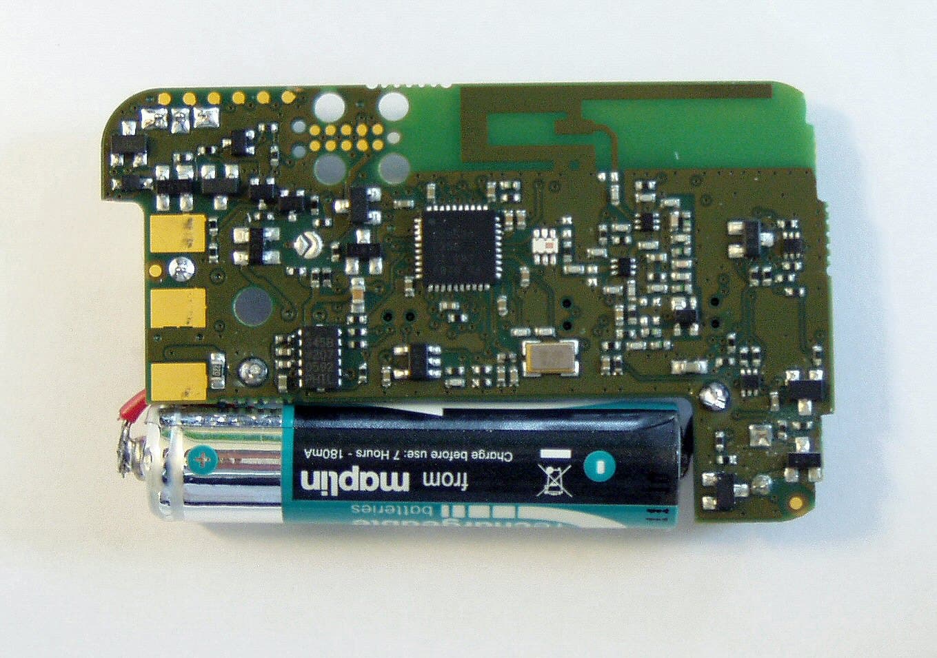
E86EKOFOB
Apr 10, 20132 way alarm and alerting device
Equipment Class
DTS - Digital Transmission System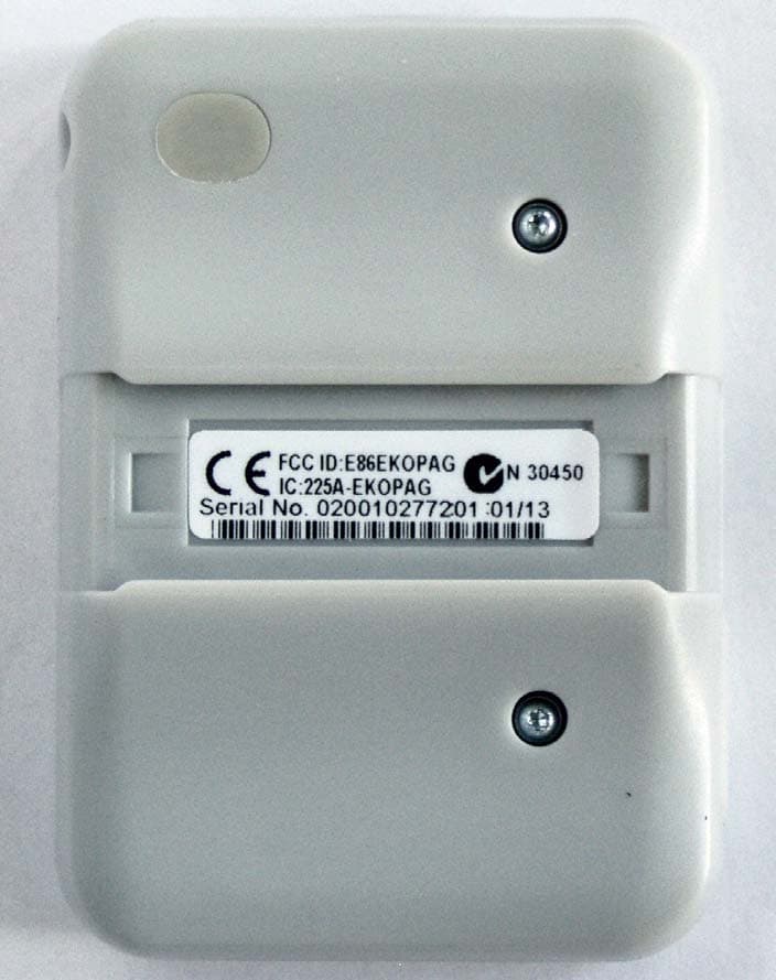
E86EKOPAG
Apr 02, 2013Alpha-numeric 2 way alarm and paging device
Equipment Class
DTS - Digital Transmission System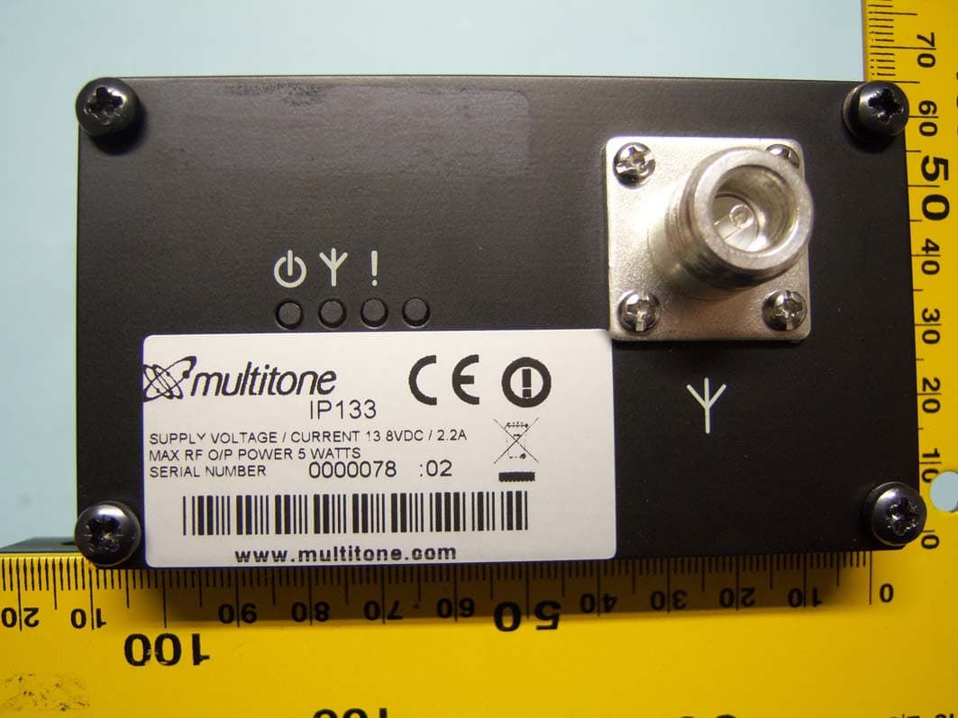
E86IP133
Feb 07, 2012Multitone I-Page � IP133
Equipment Class
TNB - Licensed Non-Broadcast Station TransmitterE86RPT503
Aug 07, 2008UHF Paging Transmitter
Equipment Class
TNB - Licensed Non-Broadcast Station Transmitter