F3JSD125V3Data Radio
Midland Radio Corporation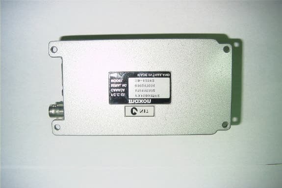
Click to zoom
Application Details
- Equipment Class
- TNB - Licensed Non-Broadcast Station Transmitter
- Date of Grant
- Oct 09, 2002
- Application Purpose
- Original Equipment
- Date of Application
- Oct 09, 2002
- Equipment Note
- Data Radio
- Frequency Range
- 216.00000000 - 220.00000000
- Company
- Midland Radio Corporation
- Country
- United States
Documents & Files
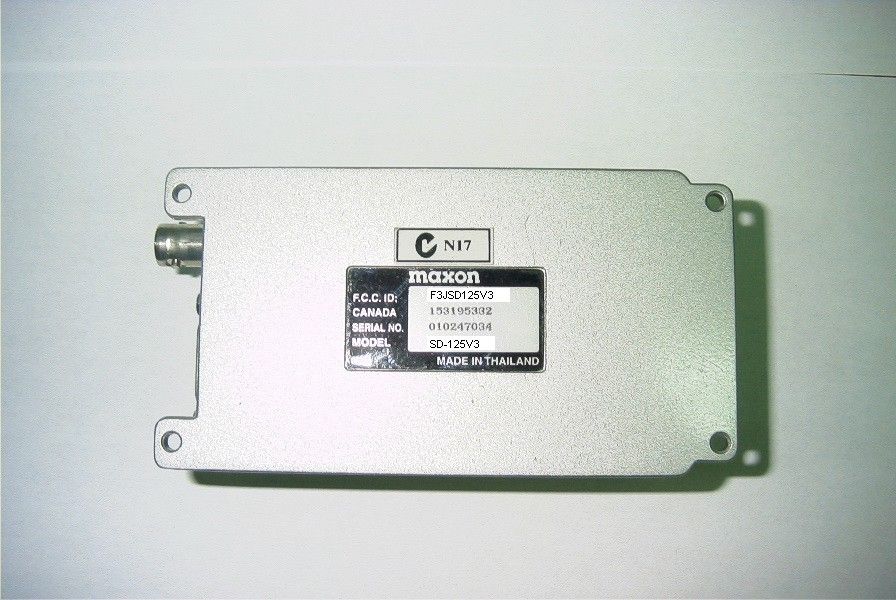
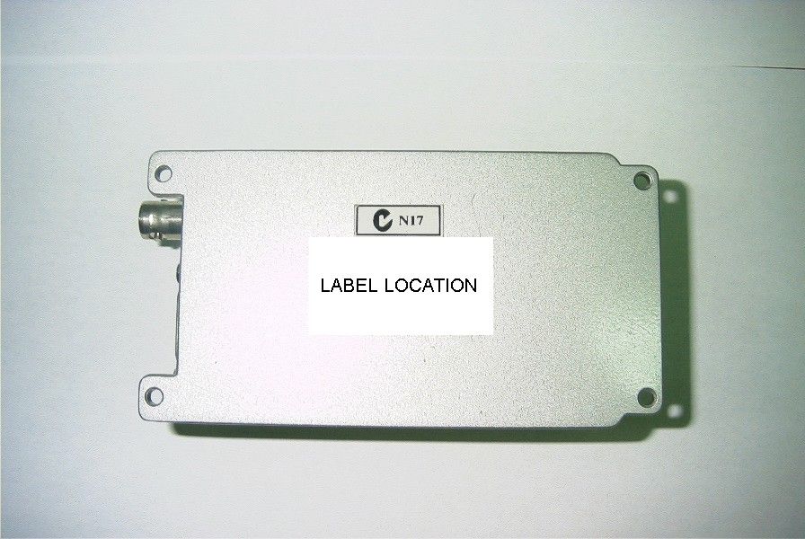
Document Text
Text extracted from the exhibit documents filed with the FCC. Open a document above to read the original.
Users Manual
Topaz3, LLC. 10828 N.W. Airworld Dr. Kansas City, MO 64153 Tel: 816-891-6320 Fax: 816-891-8815 August 2002 User Guide SD 125V3 DATA RADIO SD 125V3 Page -1- August 2002 THEORY OF OPERATION THEORY OF OPERATION The SD 125V3 radio is comprised of two PCB's (an RF PCB and a digital PCB).These boards are connected with an 18 pin female and male connector. The digitalboard is interfaced with external data equipment through the 9 pin d-sub male connec-tor, which controls the radio and data receiving and sending. DIGITAL CIRCUIT The digital circuit is charged to be control for all of the signal path and set the frequen-cies to be set and selecting the desired channel. TX-Signal circuit The TX data signal comes from Pin 2 of Con 401, and goes through U404D. The TX-signal is amplified by U406C. The TX-signal is filtered by U405A & B which is a 4'thorder low pass filter, therefore, the filtered signal supply to the RF board for TX modu-lation. RX-Signal Circuit The RX- data signal comes from the RF board, which is connected with pin 10 of Con403. The RX-signal is switched by U404A and adjusted by RV403 and amplified byU407. The amplified signal goes to pin10 of Con 401. RSSI Detector From the RF board, the RSSI (Received Signal Strength Indicator ) signal comes toU403A & B through R461. The pulse is injected from pin 5 of U403B every 1 ms andC451 is discharged. After then, it begins to be charged by R464. Simultaneously,RSSI signal is input to pin 7 of U403A and those signals are compared. The comparedsignal is output from U403A. Pin 1 and the CPU detects the pulse width. The pulsewidth is varied by RSSI DC voltage. Therefore, the CPU determines the carrier detec-tion . EEPROM RX. TX channel and RSSI detection level as well as other data from the programmerare stored in the EEPROM. The data stored is retained without power supplied. Thisis a non-volatile memory . The EEPROM may have information re-programmed orerased. U402 is an EEPROM with 2048 capacity and data is written and read serially. Channel Selector One of 16 channels may be selected using the clip switch named SW401 . SW401encodes the channel number, selected into 4-bit binary code. The binary code plusone equals the channel number. The binary code is decoded by the CPU enabling theappropriate RX or TX frequency and associated data to be selected from theEEPROM. In the binary bit of SW401, the lower 2 bits are connected to Con402. Itcauses the low 4 channels to be selected from the external equipment's. DC to DC Converter The main DC power is injected to the DC to DC converter . The DC to DC converterregulates the various input power supply voltage and outputs a constant voltage of 7.5Volts. It is a source for all of the RF and digital circuits.The DC to DC converter is formed by U801, Q801, Q802, L801 and R804. U801 is aswitch mode DC to DC Converter IC. Input DC various appears as a voltage variousthrough R804. U801 detects the voltage and controls the switching pulse. As theswitching pulses, Q801and Q802 switches the input DC of various supply voltagesand generates the constant DC of supply voltage. SD 125V3 Page -2-August 2002 THEORY OF OPERATION RF CIRCUITSTRANSMITTER The transmitter is comprised of:1. Buffer2. P.A Module3. Low Pass Filter4. Antenna Switch5. A.P.C Circuits Buffer VCO output level is -6dBm and amplified to, +6dBm. The buffer consists of Q16 andQ17 for isolation and gain. P. A . M o d u l e The P.A Module contains Q501, Q502, and Q503. Three stage amplifier Q501 ampli-fies the TX signal from +10 dBm to 100 mW. Q502 is amplified to 0.5W. Q503 ampli-fies to 3W and then matched to 50 OHMs using the L.C. network, thereby reducingthe harmonics by -30 dB. Low Pass Filter L7, L8, L11, C72, C73, C74 and C75 are the 7th order Chebyshev low pass filter.Unwanted harmonics are reduced by -70 dBc. Antenna Switch When transmitting, the diodes D5 and D6 are forward biased enabling the RF signalpassage to the antenna. D6 is shorted to ground inhibiting the RF signal to front end.In receive the diodes D5 and D6 are reversed biased passing the signal from theantenna through L13 and C83 to the front end without signal loss. Automatic Current Control (ACC) Circuits The ACC circuit consists of R109, variable resistor RV1, IC3(B) and transistors Q21and Q22. The supply current is monitored by the difference voltage on R109 (0.1Ohm). If the current varies by RF power output or other reasons, it produces somebias voltage by IC3A and Q19. The differential signal at the output of IC3 is passed toQ21 and Q22 that produces a constant power output to the antenna. RV1 is used toadjust the RF power level. RF CIRCUITS PLL SYNTHESIZER 12.8 MHz TCXO The TCXO contains the 3-stage thermistor network compensation and crystal oscilla-tor and modulation ports. Compensation is +/-5 PPM or less from -30c to +60c. PLL IC Dual Modules Prescaler Input frequency of 12.8 MHz to IC2 MC14519 pin 20 is divided to 6.25 KHz or 5 KHzby the reference counter, and then supplied to the comparator. RF signal input fromVCO is divided to 1/64 at the prescaler in IC2, divided by A and N counter in IC2 todetermine frequency steps, and then supplied to the comparator. PLL comparisonfrequency is 6.25/5KHz so that minimum programmable frequency step is 5/6.25 KHz.The A and N counter is programmed to obtain the desired frequency by serial data inthe CPU. In the comparator, the phase difference between reference and VCO signalis compared. When the phase of the reference frequency is leading , Fv is the output,but when VCO frequency is leading, Fr is the output. When Fv=Fr, phase detector outis a very small pulse. 64/65 modulus prescaler is comprised in IC2, and has two out-put ports: Port A pin 16: TX enable 2 SD 125V3 Page -3- August 2002 THEORY OF OPERATION Port B pin 15: prescaler power save control in PLL IC Pin 13 labeled test2 allows thetechnician to see the output of the dual modulus prescaler for trouble shooting pur-poses, no connection should be made to this pin. Level Shif…
Text truncated - open the document above for the full version.
Operational Description
SD 125V3 Page -1- August 2002 THEORY OF OPERATION THEORY OF OPERATION The SD 125V3 radio is comprised of two PCB's (an RF PCB and a digital PCB).These boards are connected with an 18 pin female and male connector. The digitalboard is interfaced with external data equipment through the 9 pin d-sub male connec-tor, which controls the radio and data receiving and sending. DIGITAL CIRCUIT The digital circuit is charged to be control for all of the signal path and set the frequen-cies to be set and selecting the desired channel. TX-Signal circuit The TX data signal comes from Pin 2 of Con 401, and goes through U404D. The TX-signal is amplified by U406C. The TX-signal is filtered by U405A & B which is a 4'thorder low pass filter, therefore, the filtered signal supply to the RF board for TX modu-lation. RX-Signal Circuit The RX- data signal comes from the RF board, which is connected with pin 10 of Con403. The RX-signal is switched by U404A and adjusted by RV403 and amplified byU407. The amplified signal goes to pin10 of Con 401. RSSI Detector From the RF board, the RSSI (Received Signal Strength Indicator ) signal comes toU403A & B through R461. The pulse is injected from pin 5 of U403B every 1 ms andC451 is discharged. After then, it begins to be charged by R464. Simultaneously,RSSI signal is input to pin 7 of U403A and those signals are compared. The comparedsignal is output from U403A. Pin 1 and the CPU detects the pulse width. The pulsewidth is varied by RSSI DC voltage. Therefore, the CPU determines the carrier detec-tion . EEPROM RX. TX channel and RSSI detection level as well as other data from the programmerare stored in the EEPROM. The data stored is retained without power supplied. Thisis a non-volatile memory . The EEPROM may have information re-programmed orerased. U402 is an EEPROM with 2048 capacity and data is written and read serially. Channel Selector One of 16 channels may be selected using the clip switch named SW401 . SW401encodes the channel number, selected into 4-bit binary code. The binary code plusone equals the channel number. The binary code is decoded by the CPU enabling theappropriate RX or TX frequency and associated data to be selected from theEEPROM. In the binary bit of SW401, the lower 2 bits are connected to Con402. Itcauses the low 4 channels to be selected from the external equipment's. DC to DC Converter The main DC power is injected to the DC to DC converter . The DC to DC converterregulates the various input power supply voltage and outputs a constant voltage of 7.5Volts. It is a source for all of the RF and digital circuits.The DC to DC converter is formed by U801, Q801, Q802, L801 and R804. U801 is aswitch mode DC to DC Converter IC. Input DC various appears as a voltage variousthrough R804. U801 detects the voltage and controls the switching pulse. As theswitching pulses, Q801and Q802 switches the input DC of various supply voltagesand generates the constant DC of supply voltage.
Operational Description
SD 125V3 Page -1- August 2002 THEORY OF OPERATION THEORY OF OPERATION The SD 125V3 radio is comprised of two PCB's (an RF PCB and a digital PCB).These boards are connected with an 18 pin female and male connector. The digitalboard is interfaced with external data equipment through the 9 pin d-sub male connec-tor, which controls the radio and data receiving and sending. DIGITAL CIRCUIT The digital circuit is charged to be control for all of the signal path and set the frequen-cies to be set and selecting the desired channel. TX-Signal circuit The TX data signal comes from Pin 2 of Con 401, and goes through U404D. The TX-signal is amplified by U406C. The TX-signal is filtered by U405A & B which is a 4'thorder low pass filter, therefore, the filtered signal supply to the RF board for TX modu-lation. RX-Signal Circuit The RX- data signal comes from the RF board, which is connected with pin 10 of Con403. The RX-signal is switched by U404A and adjusted by RV403 and amplified byU407. The amplified signal goes to pin10 of Con 401. RSSI Detector From the RF board, the RSSI (Received Signal Strength Indicator ) signal comes toU403A & B through R461. The pulse is injected from pin 5 of U403B every 1 ms andC451 is discharged. After then, it begins to be charged by R464. Simultaneously,RSSI signal is input to pin 7 of U403A and those signals are compared. The comparedsignal is output from U403A. Pin 1 and the CPU detects the pulse width. The pulsewidth is varied by RSSI DC voltage. Therefore, the CPU determines the carrier detec-tion . EEPROM RX. TX channel and RSSI detection level as well as other data from the programmerare stored in the EEPROM. The data stored is retained without power supplied. Thisis a non-volatile memory . The EEPROM may have information re-programmed orerased. U402 is an EEPROM with 2048 capacity and data is written and read serially. Channel Selector One of 16 channels may be selected using the clip switch named SW401 . SW401encodes the channel number, selected into 4-bit binary code. The binary code plusone equals the channel number. The binary code is decoded by the CPU enabling theappropriate RX or TX frequency and associated data to be selected from theEEPROM. In the binary bit of SW401, the lower 2 bits are connected to Con402. Itcauses the low 4 channels to be selected from the external equipment's. DC to DC Converter The main DC power is injected to the DC to DC converter . The DC to DC converterregulates the various input power supply voltage and outputs a constant voltage of 7.5Volts. It is a source for all of the RF and digital circuits.The DC to DC converter is formed by U801, Q801, Q802, L801 and R804. U801 is aswitch mode DC to DC Converter IC. Input DC various appears as a voltage variousthrough R804. U801 detects the voltage and controls the switching pulse. As theswitching pulses, Q801and Q802 switches the input DC of various supply voltagesand generates the constant DC of supply voltage.
Schematics
88 77 66 55 44 33 22 11 D D C C B B A A PTT OUTAUX OUTPTT INGNDVCCTX TONEBUSY/SQRX AUDIO IN 248 SER. INCARRIER DETECTRTSSER. OUTUNMUTEMOD OUT 1 AFO_UBVIN(12V) BUSY DETMIC IN(AF)MOD IN(DATA) SWITCHSPK OUTSERIAL OUT SERIAL IN CH_SW1CH_SW2CH_SW3CH_SW4PTTGND CARRIER_DETRX_DATATX_DATAGNDPROG_1PROG_2RTS/PTTCTSMUTE_DETPROG_MODEGNDCH_SEL1CH_SEL2+12V_IN LINK TABLELK1LK2LK3LK4LK5LK6LK7LK8LK9LK10 SD-125OPENSHORTOPENOPENOPENSHORTSHORTSHORTOPEN SHORTSHORT OPEN SHORTOPENOPENSHORTOPENOPENSHORTSHORTDM-55 of DC to DC converter (Ddcr204.sch) To DB9 connector ( Ddcr204.sch ) LK11LK12LK13 Connect to Vout Connect to VCC (5VDC) (7.5VDC) AS SHOWN SHORTOPENOPENOPENSHORT LK14LK15LK16 SD125R20.SCH 3.3 SD - 125 LOGIC CIRCUIT(VHF3) DESIGNED: H.B. LY & DON JAMIESON DRAWN: MICHAEL TRANMODIFIED BY JS PARK ON OCT.30MODIFIED BY JS LIM ON OCT.29.2001 11 Tuesday, August 27, 2002 TitleSize Document Number Rev Date: Sheet of VCC VB VB VCC 5V VB VB VB 5v VB VCC VB VB 5V 5V 5V VB 5V 5V 5V 5V 5V 5V 5V 5V 5V 5V 5V 5V 5V +- U406A LM324 32 1 411 R42410K C448 0.001 CON402DM-55123456789101112131415 + C447 33uF/35V CON401SD-125 123456789101112131415 R4122.7K R478 10K C466272 R49456K R493100k C465332 C416 0.1 + C460 10u C459220P +- U406C LM324 10 9 8 411 R48668K R485 0 R487 10K R48810K LK1 * LK2 * R467 47K R48910K +- U405DLM324 1213 14 411 +- U405CLM324 109 8 411 +- U405B LM324 56 7 411 +- U405A LM324 32 1 411 +- U403DLM339 1110 13 312 R428 10K R430 1M R429 47K R426 10K C417 0.1 LK7 LK9* LK3 * LK4* + C440 10uF C429 0.001 R423 1K C4360.1 C4140.0068 R455 22K D406 KDS193 R464 47K R480100K R42210K LK5 * LK6 * Q401KRA104S U401 68HC705C8AFB 37 36 41 42 27 32 34 35 7 6 5 4 3 2 1 44 8 9 10 11 12 13 14 15 26 25 24 23 21 20 19 18 28 31 29 30 3343 40 39 38 16 17 22 OSC1 OSC2 RESET IRQ PD0 PD5 PD7 TCAP PA0 PA1 PA2 PA3 PA4 PA5 PA6 PA7 PB0 PB1 PB2 PB3 PB4 PB5 PB6 PB7 PC0 PC1 PC2 PC3 PC4 PC5 PC6 PC7 PD1 PD4 PD2 PD3 TCMPVPP NC NC VDD NC VSS NC Q404KRC104S Q406 KRC104S U404BMC14066BD 34 5 U404D MC14066BD 1110 12 U404A MC14066BD 1 2 1314 Q403KRA104S U404C MC14066BD 89 6 7 Q408 KRC104S LK8 R44247K R44347K R44447K C43739P R500100 + C4494.7uF R46647K R468 10K LK10* C464 0.1 R425 10K R490 10 + C461 1uF R495 100K C4630.1 R447 10K U408KIA7042 1 2 3 IN G OUT R463 1.8M C439 1u R449 20K C451 0.01 C452 0.001 R45033K R465 10K R4481M X401 3.58MHz R4208.2K R473 68K C43839P R413180K R406 22K C4060.01 R410 220K C405 47p R411100K C408 47p R41910K R470 100K C415 47p C407 0.1 R40710K + C425 10u + C427100u R456 470 C424470p R453 N/A R49156K R45410K C426 0.047 R492100K C4230.047 +- U406D LM324 1213 14 411 C458120P R458 100K Q407 KTA1504S R451100K R44147K R452 100K U407 LM386N 1234 5678 GA1-IN+INGND OUT VCC B.P GA2 C4220.1 C4030.022 C404 0.1 R437 10K R475 100 + C455 4.7uF + C454 4.7uF R474 100 R477 100 R476100 C434 0.001 C430 0.001 + C4564.7uF C402 0.001 + C457 4.7uF R403 10K R433 4.7K C433 0.001 C432 0.001 C431 0.001 R43147K R434 4.7K R43247K R438 2.2K R4394.7K R4364.7K R44010K R435 10K RV403 22K t RTH401 200K C462 N/A R462NA RV4040 D404 5.6V D401 5.6V CON404OPTION 123456789 1011121314 D405 5.6V t RTH401 NA D402 5.6V +- U403A LM339 76 1 312 C4500.1 R421 10K CON403 SD-120 133456789101112131415161718 VCC GND DATA PLL LOCK PLL ENB PLL CLK MOD INPUT N/S SELECT MOD INVERT AUDIO TX ENB TX EN2 RX ENB RSSI 5V VCC BUSY GND C413 0.0033 R50510K +- U406BLM324 56 7 411 Q402 KRA104S R409 100K +- U409A LM324 32 1 411 +- U409B LM324 56 7 411 +- U409C LM324 10 9 8 411 R50147K R46010K C4180.0047 R49710K R49810K R502180K R50310K R504200K C4190.0027 C4200.01 R484 1K C442 0.001 C441 0.001 R481 1K R482 1K R483 1K C443 0.001 C446 0.001 C444 0.001 C445 0.001 C468 0.0047uF C467 0.0047uF D408 5.6V D407 5.6V D409 5.6V D410 5.6V +- U403B LM339 54 2 312 +- U403CLM339 98 14 312 R49910K R445100K C4210.001 C4120.0039 R469 100K R414100K C4100.0022 R41810K R41710K R41610K R415 10K C4090.047 C4110.0015 C4011uF R404 47K + C428 47u D403 5.6V SW4014CH RV402 0 Q405KRA104S U402 93C56 1 2 3 4 8 7 6 5 CS SK DI DO VCC N.C ORG GND R46110K R457 22K R472 120K R471220K R446 100 + C435 4.7uF 88 77 66 55 44 33 22 11 DCBA PRE OUT STREENG 48 MOD GNDB+ DATAPLL ENMODVCCGNDGNDN/S SWAUDIOTX ENTX EN2RX ENRSSI5V RX 5V TCXOVCCBUSYLOCK DTCLOCK 8 OUT1 VCO TX VCO RX MIXER MOD P.A MODULE FRONT-END CONTENTS ECO NO DATE CHECKED CHECKED APPROVED 0 SD-125RF SCHEMATIC (VHF3) MAXON D 00 Wednesday, August 28, 2002 TitleSize Document Number Rev Date: Sheet of VCCVCC TX 5V OUT2 5V TP1 TX 5V TX B2 5V VCC VCC 5V VCC VCC TX 5V 5V 5V TX 5V 5V 5V 5V TX B2 RV610K Q34KRC104 - + IC3B LM358 65 7 C9733P IC1 TK11450 + C2 10/6.3 C3 470P C1 470P C88 0.1 C510 0.01 R501 2.7K C503 0.01 C5060.01 C512 0.01 D501 KDS181 5 4 3 1 R50622 67 2 Q501 MMBR951L L5098T L501 56NH L502 1.2UH R502 8.2K R7822K Q502 BFG35 R506 100 C505 14P C507 43P C50820P R5055.1K C513 51P C502 13P C601N/F L601 4T C602 180P C605 56P L602 4T C608 390P L6034T C624 51P C515 0.01 C504 16P C603 56P C606 62P C501 3P L504 8T C514 7P R510 10K L606 4T D601 KDS226 2 GND 4 RX 5V 5 GND R60156K Q601 2SC5084 L607 4T L605 4T L604 4T C620 N/F R602 100 1 IN1 6 OUT5 R504 820 t TH1N/F R84N/F C623 27P C621 62P C615 33P C617 4P C612 470P C607 N/F C604150P C613 0.001 C609N/F C610 82P C61424P L50227NH C622220P C616 82P C122 0.01 C1230.01 C21 0.33UF(POLY) C618 12P C619 33P R509 56 C611 N/F R70 470K R69 470K R201 R100K R924.7M D9HSMS2817 43 12 T2 . T3 . C98 0.001 L6 820NH L13 5T IC5 MC3371 161 8 7 6 5 4 3 2 9 10 11 12 13 14 15 MIX IOSC1 QUAD DCOUP DCOUP LMT I VCC MIX O OSC2 AF FIL I FIL O SQ I ME DRV MUTE GND R71 1K R72 470K R66 100 R95 82K R102 22K R103 10K R104 10K R111 10K R10522K R106 22K R96 39K R112 22K R98 10K R1160D14 KDS181S R4512K D13 KD181S C135N/F C6110UF L15 150nH C9382P C1310.001 R108 56K C126 0.01 Q31KRC104 D12 KDS193 C84470P L30422UH R56 270 CF2 455HT Q32KRC104 C9216P XF1 45.1M C3180.001 R6551 L14 470NH C18 0.001 IC2MC145193F 12345678910 11121314151617181920 OSO LD *R *V VPD PD GND RX TS1 FIN FINVCCTS2VDDO/BO/AENCKDTOSI C150.1 Q5 KRA104S (PD) Q4 KRA110S (PK) C164 N/F L33 N/F C165 N/F C166 N/F L34N/…
Text truncated - open the document above for the full version.
Test Report
APPLICANT: TOPAZ3, LLC FCC ID: F3JSD125V3 REPORT #: T:\T\Topaz3LLC_F3J\911UT2\911UT2TestReport.doc TABLE OF CONTENTS LIST TABLE OF CONTENTS LIST FOR PART 90 UHF DEVICE APPLICANT: TOPAZ3, LLC FCC ID: F3JSD125V3 TEST REPORT: PAGE 1......COVER SHEET - GENERAL INFORMATION & TECHNICAL DESCR. PAGE 2......TECHNICAL DESCRIPTION CONTINUED & PAGE 3......RF POWER OUTPUT PAGE 4......MOD CHARACTERISTICS PAGE 5......AUDIO FREQUENCY RESPONSE PLOT PAGE 6-11...MODULATION LIMITING PLOTS PAGE 12.....AUDIO LOW PASS FILTER PAGE 13-14..OCCUPIED BANDWIDTH PAGE 15-18..OCCUPIED BANDWIDTH PLOTS PAGE 19.....SPURIOUS EMISSIONS AT ANTENNA TERMINALS PAGE 20.....METHOD OF MEASURING SPURIOUS EMISSIONS AT ANTENNA TERM. PAGE 21-22..FIELD STRENGTH OF SPURIOUS EMISSIONS PAGE 23.....METHOD OF MEASURING RADIATED SPURIOUS EMISSIONS PAGE 24.....FREQUENCY STABILITY PAGE 25.....SPECTRAL EFFICIENCY PROC. & PLOT PAGE 26-28..LIST OF TEST EQUIPMENT EXHIBITS CONTAINING: EXHIBIT 1.........FCC ID LABEL SAMPLE EXHIBIT 2.........LABEL LOCATION EXHIBIT 3.........SCHEMATICS EXHIBIT 4.........BLOCK DIAGRAM EXHIBIT 5.........THEORY OF OPERATION EXHIBIT 6.........EXTERNAL PHOTOGRAPHS EXHIBIT 7.........INTERNAL PHOTOGRAPHS EXHIBIT 8.........ALIGNMENT PROCEDURE EXHIBIT 9.........USERS MANUAL EXHIBIT 10........TEST SET-UP PHOTO APPLICANT: TOPAZ3, LLC FCC ID: F3JSD125V3 REPORT #: T:\T\Topaz3LLC_F3J\911UT2\911UT2TestReport.doc Page 1 of 27 GENERAL INFORMATION REQUIRED FOR TYPE ACCEPTANCE 2.1033 TOPAZ3, LLC will sell the (c)(1)(2) FCC ID: F3JSD125V3 VHF transceiver in quantity, for use under FCC RULES PART 90. 2.1033 (c) TECHNICAL DESCRIPTION 2.1033 (3) User Manual See Exhibit 14 2.1033 (4) Type of Emission: 11K25F3D For 12.5 kHz 11K0F3E For 12.5 kHz 18K0F3E For 25 kHz For 12.5 kHz Bn = 2M + 2DK M = 9,600 Bits per second D = 0.825 kHz (Peak Deviation) K = 1 Bn = 2(9600/2) + 2(0.825k)(1) = 9.6k + 1.65k = 11.25k 90.209(b)(5) AUTHORIZED BANDWIDTH = 11.25 kHz. For 12.5 kHz Bn = 2M + 2DK M = 3000 Hz D = 2.5 kHz (Peak Deviation) K = 1 Bn = 2(3000) + 2(2.5)(1) = 6k + 5k= 11k 90.209(b)(5) AUTHORIZED BANDWIDTH = 11.25 kHz. For 25 kHz Bn = 2M + 2DK M = 3000 Hz D = 6000 Hz (Peak Deviation) K = 1 Bn = 2(3000) + 2(6000) = 6k + 12k = 18k 90.209(b)(5) AUTHORIZED BANDWIDTH = 20.00 kHz. APPLICANT: TOPAZ3, LLC FCC ID: F3JSD125V3 REPORT #: T:\T\Topaz3LLC_F3J\911UT2\911UT2TestReport.doc Page 2 of 27 2.1033 (5) Frequency Range: 216-220 MHz (6) Power Range and Controls: There are NO user Power controls. (7) Maximum Output Power Rating: 0.5 Watts, into a 50 ohm resistive load. (8) DC Voltages and Current into Final Amplifier: POWER INPUT FINAL AMPLIFIER ONLY Vce = 12 Volts IC = HIGH – 1.17 A LOW - 0.53 A (9) Tune-up procedure. The tune-up procedure is given in EXHIBIT 8. 2.1033 (10) Complete Circuit Diagrams: The circuit diagram is included as EXHIBIT 2. The block diagram is included as EXHIBIT 3. (11) Function of each electron tube or semiconductor device or other active circuit device: -SEE EXHIBIT 14. (8) Instruction book. The instruction manual is included as EXHIBIT 14. (10) Description of all circuitry and devices provided for determining and stabilizing frequency is included in the circuit description in the instruction manual. 2.1033(c)(11) A photograph or drawing of the equipment identification label is shown in Exhibit 1. 2.1033(c)(12) Photographs of the equipment of sufficient clarity to reveal equipment construction and layout and label location are shown in Exhibit 6-7. 2.1033(c)(13) For equipment employing digital modulation, a detail description of the modulation technique. This UUT uses FSK to modulate the transmitter. 2.1033(c)(14) data required for 2.1046 to 2.1057 See Below 90.203(e) There are NO user controls and the frequency of this unit must be programmed using software not provided to the end user. APPLICANT: TOPAZ3, LLC FCC ID: F3JSD125V3 REPORT #: T:\T\Topaz3LLC_F3J\911UT2\911UT2TestReport.doc Page 3 of 27 2.1046(a) RF power output. RF power is measured by connecting a 50 ohm, re- sistive wattmeter to the RF output connector. With a nominal battery voltage of 7.8 VDC, and the transmitter properly adjusted the RF output measures: POWER OUTPUT INPUT POWER - HIGH: (12V)(1.17A) = 14.04 Watts INPUT POWER – LOW: (12V)(.53A) = 6.36 Watts OUTPUT POWER: HIGH - 5 Watts LOW - 1 Watts METHOD OF MEASURING RF POWER OUTPUT Transmitter 50 ohm under test Resistive Wattmeter Power Supply APPLICANT: TOPAZ3, LLC FCC ID: F3JSD125V3 REPORT #: T:\T\Topaz3LLC_F3J\911UT2\911UT2TestReport.doc Page 4 of 27 2.1047(a)(b) Modulation characteristics: AUDIO FREQUENCY RESPONSE The audio frequency response was measured in ac- cordance with TIA/EIA Specification 603. The audio frequency response curve is shown on page 5. The audio signal was fed into a dummy microphone circuit and into the microphone connector. The input required to produce 30 percent modulation level was measured. 2.1047(b) Audio input versus modulation The audio input level needed for a particular per- percentage of modulation was measured in accor- dance with TIA/EIA Specification 603. The audio input curves versus modulation are shown in pages 6-8. Curves are provided for audio input frequencies of 300, 1000, and 2500 Hz. Post Limiter Filter The filter must be between the modulation limiter and the modulated stage. At any frequency between 3 & 20 kHz the filter must have an attenuation of 60log (f/3) greater that the attenuation at 1 kHz. See the plot; page 9. APPLICANT: TOPAZ3, LLC FCC ID: F3JSD125V3 REPORT #: T:\T\Topaz3LLC_F3J\911UT2\911UT2TestReport.doc Page 5 of 27 -22 -20 -18 -16 -14 -12 -10 -8 -6 100100010000 Frequency dBmV audio response APPLICANT: TOPAZ3, LLC FCC ID: F3JSD125V3 REPORT #: T:\T\Topaz3LLC_F3J\911UT2\911UT2TestReport.doc Page 6 of 27 MODULATION LIMITING PLOT FOR 25 kHz CHANNEL SPACING – 300 Hz Modulation Limiting 0 1000 2000 3000 4000 5000 6000 7000 8000 -42-32-22-12-2 dBmV Deviation 300 Hz APPLICANT: TOPAZ3, LLC FCC ID: F3JSD125V3 REPORT #: T:\T\Topaz3LLC_F3J\911UT2\911UT2TestReport.doc…
Text truncated - open the document above for the full version.
Contact Information
Applicant
Jeff Brame(Director of Engineering)
Test Firm
Timco Engineering, Inc.S Sanders
Technical Specifications
| # | Rule Parts | Frequency Range | Power Output | Emission | Tolerance |
|---|---|---|---|---|---|
| 4 | 9 | 216 MHz - 220 MHz | 1 W | 11K0F3E | 1.5 ppm |
Other Applications from Midland Radio Corporation
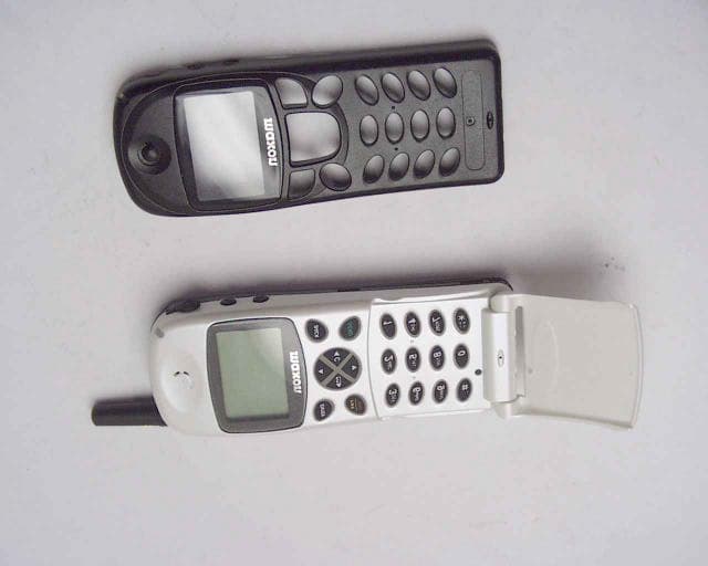
F3JMX1111
Feb 14, 2001800 MHz CDMA/AMPS Cellular Phone,Model MX-1111
Equipment Class
TNE - Licensed Non-Broadcast Transmitter Held to Ear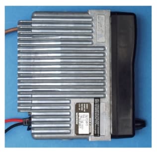
F3JSM6150V2
Sep 07, 2000VHF Mobile Transceiver
Equipment Class
TNB - Licensed Non-Broadcast Station Transmitter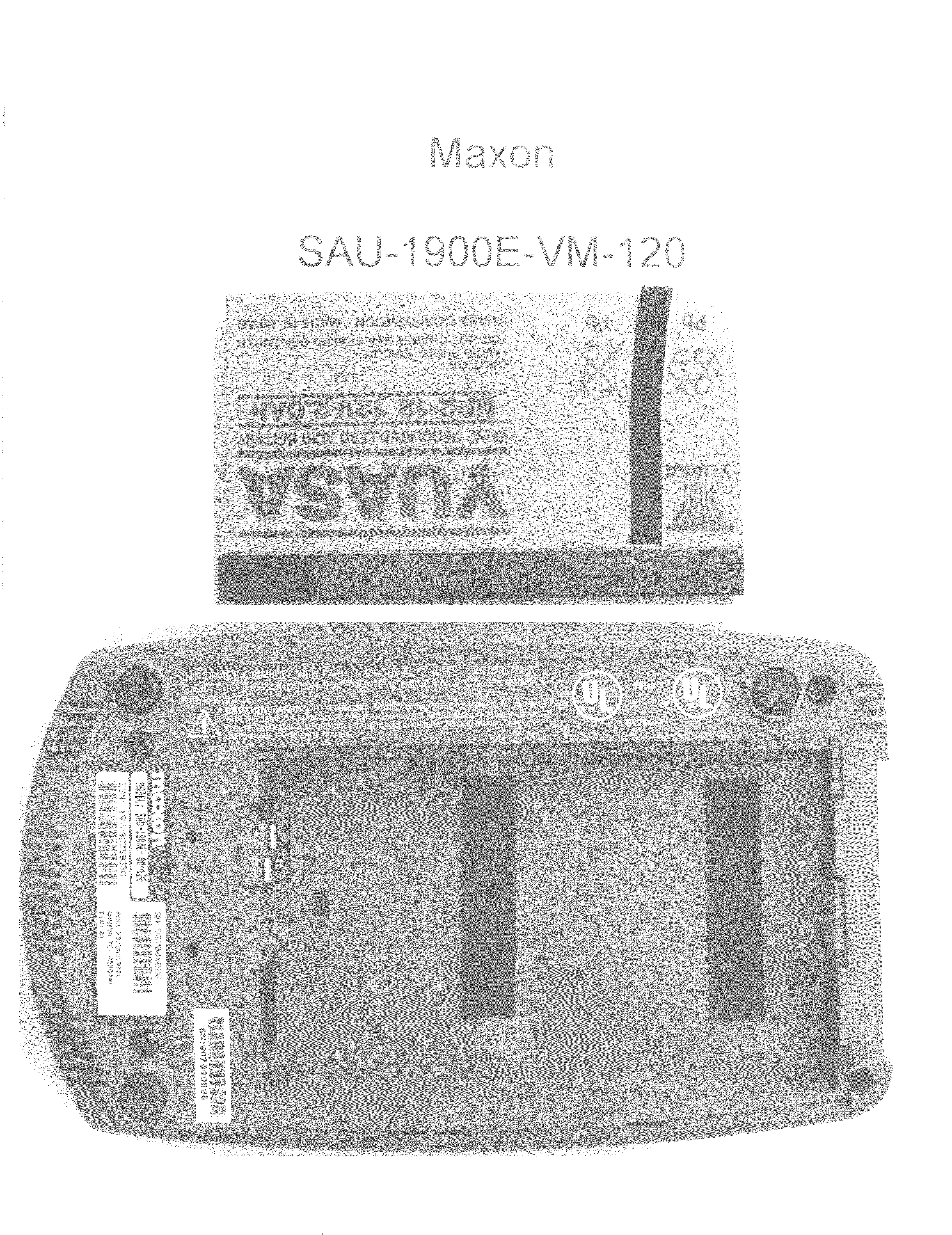
F3JSAU1900E
Aug 02, 2000PCS Band CDMA Wireless Local Loop Transceiver
Equipment Class
TNB - Licensed Non-Broadcast Station Transmitter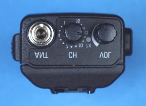
F3JSP150V2
Aug 02, 2000Portable Transceiver
Equipment Class
TNB - Licensed Non-Broadcast Station Transmitter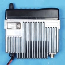
F3JSM6450U6
Mar 20, 2000UHF mobile transceiver
Equipment Class
TNB - Licensed Non-Broadcast Station Transmitter