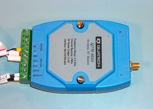
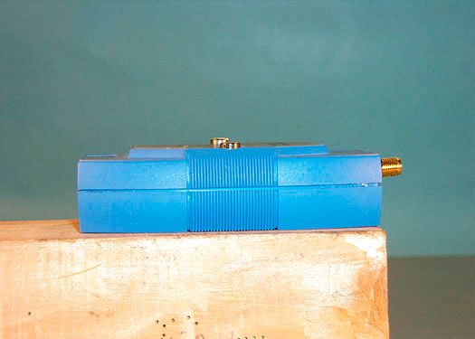
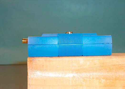
F4AQTM85242000Radio RF Modem, QTM-8524
B plus B SmartWorx, Inc.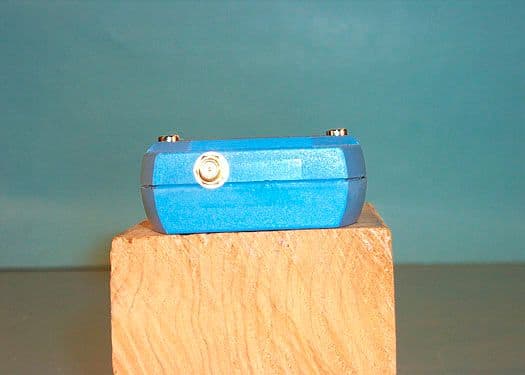
Click to zoom
Application Details
- Equipment Class
- DSS - Part 15 Spread Spectrum Transmitter
- Date of Grant
- Feb 20, 2001
- Application Purpose
- Original Equipment
- Date of Application
- Jan 04, 2001
- Equipment Note
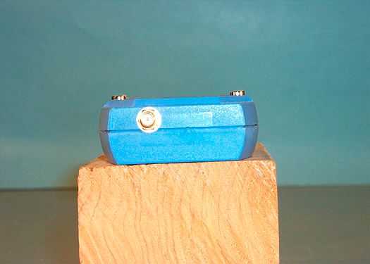
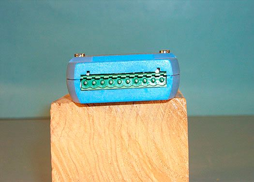
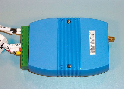
- Radio RF Modem, QTM-8524
- Frequency Range
- 2426.00000000 - 2458.00000000
- Company
- B plus B SmartWorx, Inc.
- Country
- United States
Documents & Files
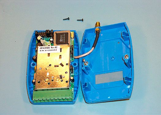
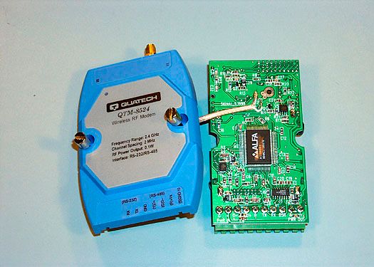
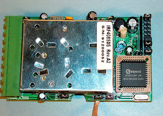
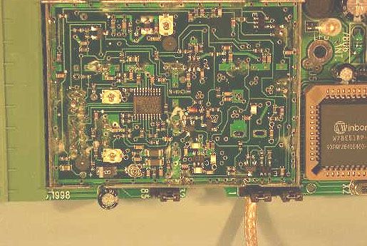
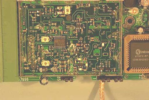
Document Text
Text extracted from the exhibit documents filed with the FCC. Open a document above to read the original.
Users Manual
QTM-8524 2.4 GHz RF Radio Modem Module Users Manual QUATECH, Inc.TEL: (330) 434-3154 662 Wolf Ledges PkwyFAX: (330) 434-1409 Akron, Ohio 44311http://www.quatech.com WIRELESS MODEM MODULE FOR QTM-8000 SERIES SYSTEMS QTM-8524 User’s Manual Revision 1.0 PN Warranty Information Quatech Inc. warrants the QTM-8524 to be free of defects for one (1) year from the date of purchase. Quatech Inc. will repair or replace any system component that fails to perform under normal operating conditions in accordance with the procedures outlined in this document, provided the failure occurs during the one year warranty period. Any damage resulting from improper installation, operation or general misuse voids all warranty rights. No representation is made regarding the suitability of this product for any particular purpose. Please complete the following information and retain for your records. Date of Purchase: Model Number: QTM-8524 Product: 2.4 GHz RF Radio Modem_ Serial Number: All products returned to Quatech for either warranty or non- warranty repair MUST be assigned a Returned Material Authorization (RMA) number prior to shipment. This RMA number must be clearly marked on the exterior of the product’s return packaging and in any correspondence to ensure proper routing and prompt attention. To obtain an RMA number, contact the Quatech Technical Support Department at 1-800-553-1170 or (330) 434-3154. In order to prevent damage to returned merchandise during shipment, please package electronic components in anti-static/shock proof materials. For warranty repair/returns, please have the following information available when contacting the Technical Support department: 1. Model number and serial number of the product under warranty, 2. Repair instructions and/or specific description of the problem. For non-warranty repairs or upgrades, contact the Technical Support department for current repair charges and please have the following information available: 1. Purchase order number to cover the cost of the service, 2. Model number and serial number of the product, 3. Repair or upgrade instructions relative to the product. Notice The information contained in this document cannot be reproduced in any form without the written consent of Quatech Inc. Any software programs accompanying this document can be used only in accordance with any licensing agreement(s) between the purchaser and Quatech Inc. Quatech Inc. reserves the right to change this documentation or the product to which it refers at any time and without notice. The authors have taken due care in the preparation of this document and any associated software program(s). Every attempt has been made to ensure accuracy and completeness. Under no circumstances will Quatech Inc. be liable for damages of any kind, incidental or consequential, in regard to or arising from the performance or form of the materials presented herein or in any software program(s) that may accompany this document. Quatech Inc. encourages and appreciates feedback concerning this document. Please send any written comments to the Technical Support Department at the address listed on the cover of this manual. Table of Contents 1.Introduction9 1.1 Available QTM-8000 Series Modules10 1.2QTM-8000 Series Common Features11 1.3QTM-8000 Series Wireless Networks12 1.3.1Disadvantages of Conventional Two-Wire RS-485 Networks13 1.3.2The QTM-8000 Series Network Advantage14 1.3.3Operation Principle15 1.3.4Supporting Multiple Baud Rates16 1.4QTM-8000 Series Module dimensions17 2.QTM-8524 Specifications20 2.1Pin Assignments20 2.2QTM-8524 Module Specifications21 2.3QTM-8524 Block Diagram22 2.4QTM-8524 Disassembly22 2.5QTM-8524 Jumper Settings24 2.6QTM-8524 Basic Wire Connections26 2.6.1RS-232 Connection Between PC and QTM-852426 2.6.2Connecting QTM-8000 Modules to the QTM-852426 3.Antennas27 3.1QTM-8524 Antenna Options27 3.1.1QTM-24ANT-SW Specifications27 3.1.2QTM-24ANT-C Specifications28 3.2Connecting Antennas to QTM-8524 Modules29 3.2.1Site Selection29 3.2.2Installation29 3.2.3Connection29 3.3Mounting External Antennas30 3.3.1Mounting the QTM-24ANT-SW30 3.3.2Mounting the QTM-24ANT-C32 3.3.3RF Safety34 4.Configuration34 4.1RS-232 or RS-485 Configuration34 4.2Half-Duplex and Full-Duplex Operation34 4.3Synchronous and Asynchronous Communication35 4.4Configuration Modes36 4.4.1Mode 1: Full-Duplex, Synchronous37 4.4.2Mode 2: Half-Duplex, Synchronous38 4.4.3Mode 3: Full-Duplex, Asynchronous39 5.Application Examples40 5.1Peer-to-Peer Communication (Mode 1)40 5.2Interfacing with QTM-8000 Modules (Mode 1)41 5.3Multiple PC Communication (Mode 2)42 5.4Asynchronous Communication (Mode 3)43 6.Approvals44 List of Figures 1.3QTM-8000 Series Network with Multiple Baud Rates and Multiple Data Formats12 1.3.2.1Single Baud Rate QTM-8000 Wireless Network13 1.3.2.2Multi-Baud Rate Wireless QTM-8000 Network14 1.4.1QTM-8000 Series Front, Side, Rear and Top Views17 1.4.2QTM-8000 Series DIN Rail Mounting18 1.4.3QTM-8000 Series Panel Mounting19 2.3QTM-8524 Block Diagram22 2.4Disassembling the QTM-852423 2.5QTM-8524 Jumper Settings25 2.5.1Connecting QTM-8524 to DB-9 Serial Cable26 2.5.2Connecting QTM-8524 to QTM-8000 I/O Modules26 3.1.1QTM-24ANT-SW Transmission Pattern27 3..1.2QTM-24ANT-C Transmission Pattern28 3.3.1.1Mounting the QTM-24ANT-SW Steps 1-630 3.3.1.2Mounting the QTM-24ANT-SW Step 731 3.3.2.1Installing the QTM-24ANT-C Ceiling Mount Bracket33 3.3.2.2Connecting the QTM-24ANT-C Antenna to the Bracket33 5.1QTM-8524 Peer-to-Peer Communication40 5.2QTM-8524 as part of a QTM-8000 Series I/O Network41 5.3QTM-8524 Modules Used to Network Multiple PCs42 5.4QTM-8524 Modules in an Asynchronous Network43 Quatech QTM-8524 Manual 9 1. Introduction The QTM-8000 Series of modules is comprised of analog and digital I/O modules designed for a wide variety of data ac- quisition and signal conditioning functions. These modules are designed for an RS-485 communication network, and re- quire an RS-485 to RS-232 converter in order to be acce…
Text truncated - open the document above for the full version.
Users Manual
QTM-8524 2.4 GHz RF Radio Modem Module Users Manual QUATECH, Inc.TEL: (330) 434-3154 662 Wolf Ledges PkwyFAX: (330) 434-1409 Akron, Ohio 44311http://www.quatech.com WIRELESS MODEM MODULE FOR QTM-8000 SERIES SYSTEMS QTM-8524 User’s Manual Revision 1.0 PN Warranty Information Quatech Inc. warrants the QTM-8524 to be free of defects for one (1) year from the date of purchase. Quatech Inc. will repair or replace any system component that fails to perform under normal operating conditions in accordance with the procedures outlined in this document, provided the failure occurs during the one year warranty period. Any damage resulting from improper installation, operation or general misuse voids all warranty rights. No representation is made regarding the suitability of this product for any particular purpose. Please complete the following information and retain for your records. Date of Purchase: Model Number: QTM-8524 Product: 2.4 GHz RF Radio Modem_ Serial Number: All products returned to Quatech for either warranty or non- warranty repair MUST be assigned a Returned Material Authorization (RMA) number prior to shipment. This RMA number must be clearly marked on the exterior of the product’s return packaging and in any correspondence to ensure proper routing and prompt attention. To obtain an RMA number, contact the Quatech Technical Support Department at 1-800-553-1170 or (330) 434-3154. In order to prevent damage to returned merchandise during shipment, please package electronic components in anti-static/shock proof materials. For warranty repair/returns, please have the following information available when contacting the Technical Support department: 1. Model number and serial number of the product under warranty, 2. Repair instructions and/or specific description of the problem. For non-warranty repairs or upgrades, contact the Technical Support department for current repair charges and please have the following information available: 1. Purchase order number to cover the cost of the service, 2. Model number and serial number of the product, 3. Repair or upgrade instructions relative to the product. Notice The information contained in this document cannot be reproduced in any form without the written consent of Quatech Inc. Any software programs accompanying this document can be used only in accordance with any licensing agreement(s) between the purchaser and Quatech Inc. Quatech Inc. reserves the right to change this documentation or the product to which it refers at any time and without notice. The authors have taken due care in the preparation of this document and any associated software program(s). Every attempt has been made to ensure accuracy and completeness. Under no circumstances will Quatech Inc. be liable for damages of any kind, incidental or consequential, in regard to or arising from the performance or form of the materials presented herein or in any software program(s) that may accompany this document. Quatech Inc. encourages and appreciates feedback concerning this document. Please send any written comments to the Technical Support Department at the address listed on the cover of this manual. Table of Contents 1.Introduction9 1.1 Available QTM-8000 Series Modules10 1.2QTM-8000 Series Common Features11 1.3QTM-8000 Series Wireless Networks12 1.3.1Disadvantages of Conventional Two-Wire RS-485 Networks13 1.3.2The QTM-8000 Series Network Advantage14 1.3.3Operation Principle15 1.3.4Supporting Multiple Baud Rates16 1.4QTM-8000 Series Module dimensions17 2.QTM-8524 Specifications20 2.1Pin Assignments20 2.2QTM-8524 Module Specifications21 2.3QTM-8524 Block Diagram22 2.4QTM-8524 Disassembly22 2.5QTM-8524 Jumper Settings24 2.6QTM-8524 Basic Wire Connections26 2.6.1RS-232 Connection Between PC and QTM-852426 2.6.2Connecting QTM-8000 Modules to the QTM-852426 3.Antennas27 3.1QTM-8524 Antenna Options27 3.1.1QTM-24ANT-SW Specifications27 3.1.2QTM-24ANT-C Specifications28 3.2Connecting Antennas to QTM-8524 Modules29 3.2.1Site Selection29 3.2.2Installation29 3.2.3Connection29 3.3Mounting External Antennas30 3.3.1Mounting the QTM-24ANT-SW30 3.3.2Mounting the QTM-24ANT-C32 3.3.3RF Safety34 4.Configuration34 4.1RS-232 or RS-485 Configuration34 4.2Half-Duplex and Full-Duplex Operation34 4.3Synchronous and Asynchronous Communication35 4.4Configuration Modes36 4.4.1Mode 1: Full-Duplex, Synchronous37 4.4.2Mode 2: Half-Duplex, Synchronous38 4.4.3Mode 3: Full-Duplex, Asynchronous39 5.Application Examples40 5.1Peer-to-Peer Communication (Mode 1)40 5.2Interfacing with QTM-8000 Modules (Mode 1)41 5.3Multiple PC Communication (Mode 2)42 5.4Asynchronous Communication (Mode 3)43 6.Approvals44 List of Figures 1.3QTM-8000 Series Network with Multiple Baud Rates and Multiple Data Formats12 1.3.2.1Single Baud Rate QTM-8000 Wireless Network13 1.3.2.2Multi-Baud Rate Wireless QTM-8000 Network14 1.4.1QTM-8000 Series Front, Side, Rear and Top Views17 1.4.2QTM-8000 Series DIN Rail Mounting18 1.4.3QTM-8000 Series Panel Mounting19 2.3QTM-8524 Block Diagram22 2.4Disassembling the QTM-852423 2.5QTM-8524 Jumper Settings25 2.5.1Connecting QTM-8524 to DB-9 Serial Cable26 2.5.2Connecting QTM-8524 to QTM-8000 I/O Modules26 3.1.1QTM-24ANT-SW Transmission Pattern27 3..1.2QTM-24ANT-C Transmission Pattern28 3.3.1.1Mounting the QTM-24ANT-SW Steps 1-630 3.3.1.2Mounting the QTM-24ANT-SW Step 731 3.3.2.1Installing the QTM-24ANT-C Ceiling Mount Bracket33 3.3.2.2Connecting the QTM-24ANT-C Antenna to the Bracket33 5.1QTM-8524 Peer-to-Peer Communication40 5.2QTM-8524 as part of a QTM-8000 Series I/O Network41 5.3QTM-8524 Modules Used to Network Multiple PCs42 5.4QTM-8524 Modules in an Asynchronous Network43 Quatech QTM-8524 Manual 9 1. Introduction The QTM-8000 Series of modules is comprised of analog and digital I/O modules designed for a wide variety of data ac- quisition and signal conditioning functions. These modules are designed for an RS-485 communication network, and re- quire an RS-485 to RS-232 converter in order to be acce…
Text truncated - open the document above for the full version.
Cover Letter(s)
662 Wolf Ledges Parkway Akron,Ohio 44311 1 800 533-1170 330 434-3154 Fax: 330 434-1409 http://www.quatech.com Federal Communications Commission 7435 Oakland Mills Road Columbia, MD 21046 Gentlemen: This letter is to comply with Section 0.457(d)(2)(i) pertaining to confidential material. Quatech Inc. would like the following documents regarding this submission to be kept confidential. 1. All drawings, schematics and block diagrams. Specifically: a. Drawing QTM8524_BD b. Drawing QTM8524_SCH, sheets 1 and 2 2. Pages 1-11 of the expository document (“expository.pdf”). The above material contains trade secrets, vendor data or technical data, which would customarily be guarded from competitors. We do not want these documents to be accessible to the general public. Sincerely, Steven D. Runkel President/ CEO Quatech Inc.
Cover Letter(s)
Correspondence to Request 10865 FCC ID F4AQTM85242000 1. Revised Test Report FC00-108A has been uploaded. 2. A file has been uploaded to show the MPE Calculations 3. A revised User’s Manual has been uploaded to include the warning statement on page34.
ID Label/Location Info
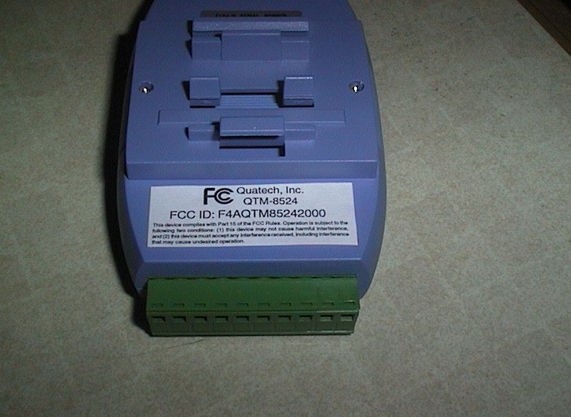
FCC ID: F4AQTM85242000 Quatech, Inc. QTM-8524 This device complies with Part 15 of the FCC Rules. Operation is subject to thefollowing two conditions: (1) this device may not cause harmful interference,and (2) this device must accept any interference received, including interferencethat may cause undesired operation. <-----------------2”-----------------> <----.75”---->
RF Exposure Info
CONFIDENTIAL MPE Calculations for the QTM-8524 The Maximum Permissible Exposure (MPE) for the QTM-8524 shall be calculated for two case antennas. The first is a wall mounted patch antenna with a gain of 7.5dBi, and the second is a ceiling mounted monopole antenna with a gain of 3.0dBi. The equation used in this calculation is shown below: S= PG 4 ✜R 2 Where S = power density in mW/cm 2 P = transmitter power in mW G = numeric antenna gain over isotropic Solving this equation for R: R= PG 4✜S From OET Bulletin 65, Appendix A, Table B, General Population/Uncontrolled Exposure, S =1 in the 2.4GHz range. The transmitter power, P, is 707mW. Results of the calculations are shown below: Because the results are less than the required minimum 20cm distance, the user’s manual will reflect the 20cm distance to ensure maximum safety for end users and the general public. Antenna Type Log Gain (dBi) Numeric GainMPE (cm) Patch7.55.6217.78 Monopole3210.6
Test Report
Page 1 of 59 Report No: FC00-108 CERTIFICATION TEST REPORT FOR THE RADIO RF MODEM, QTM-8524 FCC PART 15 SUBPART C SECTIONS 15.247/15.207/15.209 COMPLIANCE DATE OF ISSUE: NOVEMBER 8, 2000 PREPARED FOR: Quatech Inc. 662 Wolf Ledges Parkway Akron, Ohio 44311 P.O. No: 14258 W.O. No: 74623 PREPARED BY: Helen Parrish CKC Laboratories, Inc. 5473A Clouds Rest Mariposa, CA 95338 Date of test: October 18-20, 2000 Report No: FC00-108 DOCUMENTATION CONTROL: _____________________________ Tracy Phillips Documentation Control Supervisor CKC Laboratories, Inc. APPROVED BY: _____________________________ Dennis Ward Director of Laboratories CKC Laboratories, Inc. This report contains a total of 59 pages and may be reproduced in full only. Partial reproduction may only be done with the written consent of CKC Laboratories, Inc. Page 2 of 59 Report No: FC00-108 TABLE OF CONTENTS Administrative Information ............................................................................................. 4 Summary Of Results........................................................................................................ 5 Equipment Under Test (EUT) Description...................................................................... 5 Measurement Uncertainty................................................................................................ 5 Peripheral Devices ........................................................................................................... 6 Report Of Measurements................................................................................................. 7 Table 1: Peak Output Power Emission Levels .................................................... 7 Table 2: Spurious Emissions – RF Antenna Conducted...................................... 8 Table 3: Spurious Emissions – Radiated (Patch)................................................. 9 Table 4: Spurious Emissions – Radiated (Monopole) ......................................... 10 Table 5: Peak Power Spectral Density ................................................................ 11 Table 6: Six Highest Conducted Emission Levels .............................................. 12 Table A: List Of Test Equipment .................................................................................... 13 EUT Setup .......................................................................................................................14 Radiated Emissions ............................................................................................. 14 Conducted Emissions .......................................................................................... 14 EUT Testing .................................................................................................................... 15 Radiated Emissions ............................................................................................. 15 Conducted Emissions .......................................................................................... 15 Test Instrumentation And Analyzer Settings................................................................... 16 Table B: Analyzer Bandwidth Settings Per Frequency Range............................ 16 Spectrum Analyzer Detector Functions............................................................... 17 Peak ......................................................................................................... 17 Quasi-Peak............................................................................................... 17 Average.................................................................................................... 17 Test Methods ................................................................................................................... 17 Transmitter Characteristics.............................................................................................. 18 15.247(a)(2) Occupied Bandwidth – Direct Sequence ........................................ 18 List of Test Equipment Used for Occupied Bandwidth Test............................... 18 FCC Part 15.247(a)(2) Occupied Bandwidth Plot – Direct Sequence ................ 19 FCC Part 15.247(a)(2) Occupied Bandwidth Plot – Direct Sequence ................ 20 FCC Part 15.247(a)(2) Occupied Bandwidth Plot – Direct Sequence ................ 21 FCC Part 15.247(a)(2) Highest Channel Band Edge Plot ................................... 22 FCC Part 15.247(a)(2) Lowest Channel Band Edge Plot .................................... 23 15.247(b) Power Output ...................................................................................... 24 List of Test Equipment Used for Power Output Test .......................................... 24 15.247(d) Peak Power Spectral Density .............................................................. 25 List of Test Equipment Used for Peak Power Spectral Density Test .................. 25 FCC Part 15.247(d) Peak Power Spectral Density Plot....................................... 26 FCC Part 15.247(d) Peak Power Spectral Density Plot....................................... 27 FCC Part 15.247(d) Peak Power Spectral Density Plot....................................... 28 Page 3 of 59 Report No: FC00-108 Sample Calculations ........................................................................................................ 29 Appendix A: Information About The Equipment Under Test......................................... 30 I/O Ports............................................................................................................... 31 Crystal Oscillators ............................................................................................... 31 Printed Circuit Boards ......................................................................................... 31 Required EUT Changes To Comply.................................................................... 31 Cable Information..................................…
Text truncated - open the document above for the full version.
Test Report
CONFIDENTIAL Quatech Inc. 662 Wolf Ledges Parkway Akron, Ohio 44311 (800) 553-1170 (330) 434-3154 (330) 434 –1409 FAX http://www.quatech.com File:processing gain.DOC PRODUCT NAME: QTM-8524 NAME OF TEST: The Processing Gain of a Direct Sequence System Processing Gain Measurement and Calculation The processing gain of this spread spectrum system was measured using the CW jamming method. Figure 1 illustrates the measurement setup. The output power of the spread spectrum transmitter is fixed and the output power of jammer is adjustable. The frequency of jammer was stopped through the pass band of nominal channel in 50khz. In each frequency step of the jammer, the output power of jammer is adjusted to cause the Bit Error Rate (BER) to be 1.0*10 -3 . The power levels are recorded to calculate the J/S as shown in Table 1. The processing gain Gp was calculated using the formula: Gp = (S/N) 0 + Mj + Lsys where S/N is the signal to noise ratio. Mj is the jammer to signal ratio (J/S), and Lsys is the system loss. For the BER = 1.0*10 -3 , the Eh/No of the GMSK discriminator (BT=0.5) is about 14dB. Due to using the hard-decision receiver, the Eh/No will be 17dB and then signal to moise ratio (S/N) should be 15.24dB. From Table 1, the minimum J/S ratio is -4.4dB. And assume the system loss is 1dB. Therefore, the processing gain is calculated below: Gp = S/N = Mj + Lsys = 15.24 + (-4.4) + 1 = 11.84 CONFIDENTIAL Quatech Inc. 662 Wolf Ledges Parkway Akron, Ohio 44311 (800) 553-1170 (330) 434-3154 (330) 434 –1409 FAX http://www.quatech.com File:processing gain.DOC BER Meter HP3784A Digital Transmission Analyzer Spread spectrum transmitter Power Meter HP4378 Spread Spectrum Receiver Jammer HP8625A Synthesized RF Sweeper Power Divider 20 dB Attenuator 10 dB Attenuator Figure 1: Processing Gain Measurement Setup Rx CLK Rx DATA Tx CLK Tx DATA Power Combiner
Test Report
Page 1 of 4 Report No: FC00-108A ADDENDUM TO TEST REPORT FC00-1008 FOR THE RADIO RF MODEM, QTM-8524 FCC PART 15 SUBPART C SECTIONS 15.247/15.207/15.209 COMPLIANCE DATE OF ISSUE: FEBRUARY 13, 2001 PREPARED FOR: Quatech Inc. 662 Wolf Ledges Parkway Akron, Ohio 44311 P.O. No: 14258 W.O. No: 74623 PREPARED BY: Joyce Walker CKC Laboratories, Inc. 5473A Clouds Rest Mariposa, CA 95338 Date of test: October 18-20, 2000 Report No: FC00-108A DOCUMENTATION CONTROL: _____________________________ Tracy Phillips Documentation Control Supervisor CKC Laboratories, Inc. APPROVED BY: _____________________________ Dennis Ward Director of Laboratories CKC Laboratories, Inc. This report contains a total of 4 pages and may be reproduced in full only. Partial reproduction may only be done with the written consent of CKC Laboratories, Inc. Page 2 of 4 Report No: FC00-108A TABLE OF CONTENTS Administrative Information .............................................................................................3 Summary Of Results ........................................................................................................4 Equipment Under Test (EUT) Description ......................................................................4 Measurement Uncertainty ................................................................................................4 Page 3 of 4 Report No: FC00-108A CKC Laboratories, Inc. has Certificates of Accreditation from the following agencies: DATech (Germany); A2LA (USA); FCC (USA); VCCI (Japan); BSMI (Taiwan); HOKLAS (Hong Kong). CKC Laboratories, Inc. has Letters of Acceptance through an MRA for the following agencies: ACA/NATA (Australia); SABS (South Africa); SWEDAC (Sweden); TUV Rheinland-Germany; TUV Rheinland- Korea; TUV Rheinland-Russia; Radio Communication Agency (RA); NEMKO (Norway). ADMINISTRATIVE INFORMATION DATE OF TEST: October 18-20, 2000 PURPOSE OF TEST: To demonstrate the compliance of the Radio RF Modem, QTM-8524, with the requirements for FCC Part 15.247, 15.207 and 15.209 devices. The addendum removes the + 2 dB from the maximum rated power output listed on the Summary page . MANUFACTURER: Quatech Inc. 662 Wolf Ledges Parkway Akron, Ohio 44311 REPRESENTATIVE: Diane Glaze, Quality Manager TEST LOCATION: CKC Laboratories, Inc. 22105 Wilson River Hwy Tillamook, OR 97141 TEST PERSONNEL: Mike Wilkinson TEST METHOD: ANSI C63.4 1992 & FCC 97-114 Appendix C FREQUENCY RANGE TESTED: 450 kHz – 25 GHz EQUIPMENT UNDER TEST: Radio RF Modem Manuf: Quatech Inc. Model: QTM-8524 Serial: IT240EXT99KI0139 FCC ID: F4AQTM85242000 (pending) Monopole Antenna Manuf: Quatech Inc. Model: QTM-24ANT-C Serial: NONE FCC ID: N/A Patch Array Antenna Manuf: Quatech Inc. Model: QTM-24ANT-SW Serial: NONE FCC ID: N/A Page 4 of 4 Report No: FC00-108A SUMMARY OF RESULTS The Quatech Inc. Radio RF Modem, QTM-8524, was tested in accordance with ANSI C63.4 1992 and FCC 97-114 Appendix C for compliance with FCC Part 15.247, 15.207 and 15.209. As received, the above equipment was found to be fully compliant with the limits of FCC Part 15.247, 15.207 and 15.209. The results in this report apply only to the items tested, as identified herein. EQUIPMENT UNDER TEST (EUT) DESCRIPTION 2.4GHz, DSSS data modem with RS-232 and RS-422/485 I/O interfaces. No cabling provided for RS-422/485 interfacing. Spread Spectrum Method: Direct Sequence Tx/Rx Frequency Range: 2426 to 2458 MHz Number Of Channels: 8 Channels Jumper Select Channel Separation: 2.048 MHz Max RF Output Power: 28.5 dBm (.707 watts) Type of Antenna:1) Patch 2) Monopole Modulation Type: Gaussian Minimum Shift Keying (GMSK) MEASUREMENT UNCERTAINTY Associated with data in this report is a ±4dB measurement uncertainty. TEMPERATURE AND HUMIDITY DURING TESTING The temperature during testing was within +15°C and + 35°C. The relative humidity was between 20% and 75%.
Contact Information
Applicant
Mike McNatt(Compliance Engineer)
Non-Technical Contact
CKC Laboratories, Inc.Joyce Walker
[email protected]1-800-500-4362
Test Firm
CKC Laboratories, Inc.Steve Behm
Technical Specifications
| # | Rule Parts | Frequency Range | Power Output |
|---|---|---|---|
| 1 | 15C | 2.43 GHz - 2.46 GHz | 707.00 mW |
Other Applications from B plus B SmartWorx, Inc.
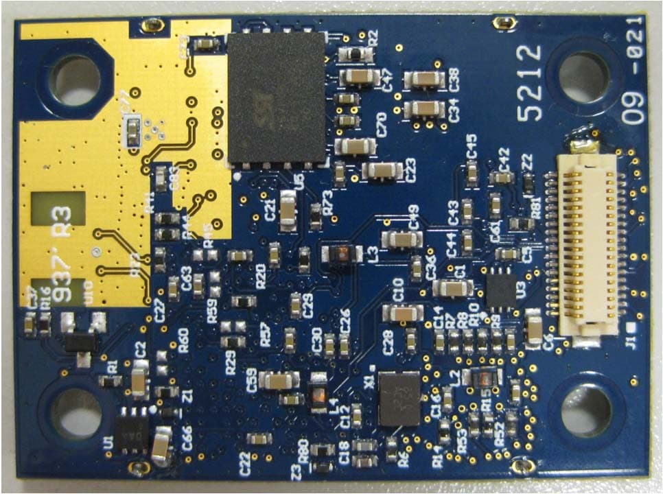
F4AWLNN551
Apr 30, 2013Zonda 801.11 a/b/g/n WLAN
Equipment Class
DTS - Digital Transmission System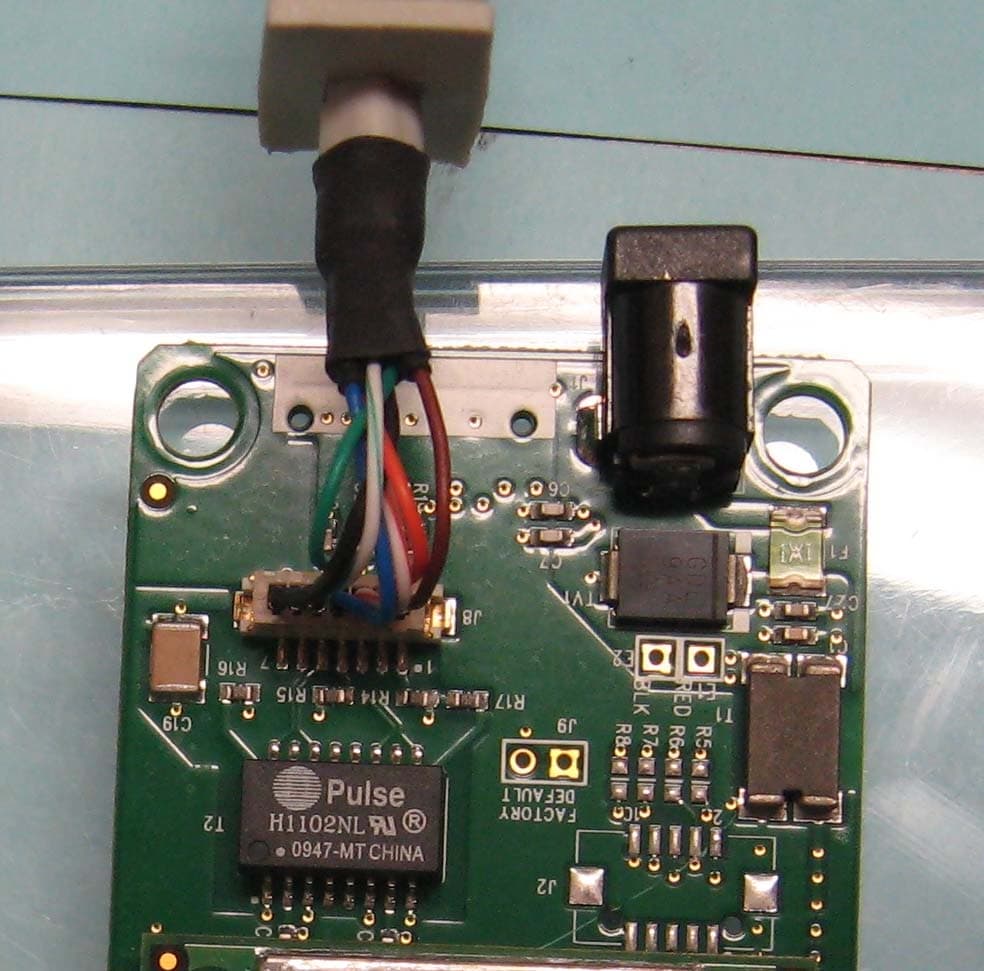
F4AWLNG551
Apr 18, 2011Ethernet Device Adapter
Equipment Class
DTS - Digital Transmission System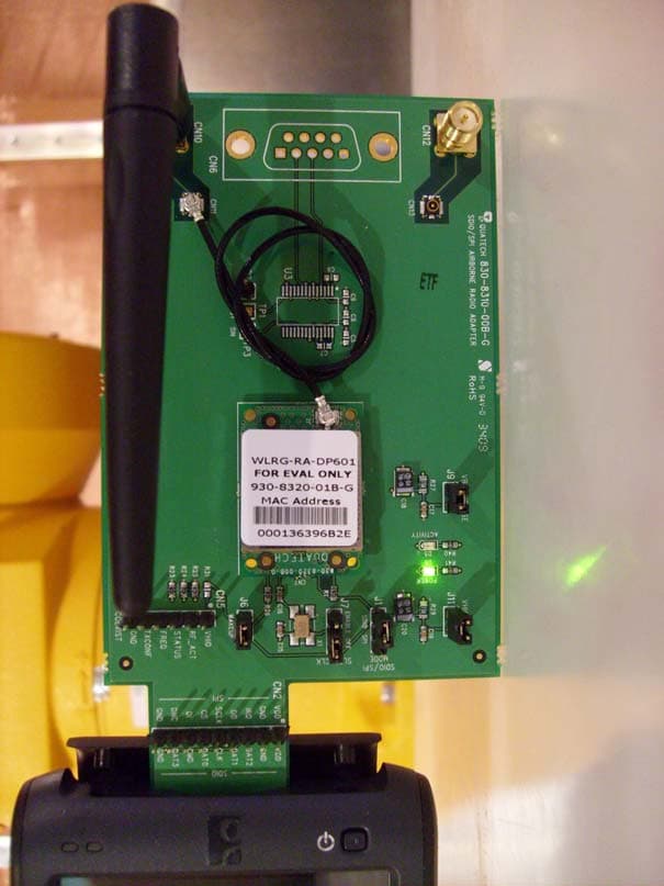
F4AWLRG601
Jun 27, 2010802.11 b/g radio module
Equipment Class
DTS - Digital Transmission System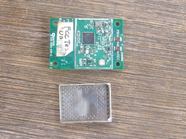
F4AWLNG1
Jul 16, 2006802.11 b/g module
Equipment Class
DTS - Digital Transmission System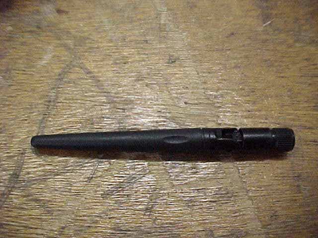
F4ATHINQ1
Mar 15, 2005ThinQ SDS
Equipment Class
DTS - Digital Transmission System