FDI-09101727-0Wireless LAN Card
BUFFALO INC.
Click to zoom
Application Details
- Equipment Class
- DSS - Part 15 Spread Spectrum Transmitter
- Date of Grant
- Dec 19, 2001
- Application Purpose
- Original Equipment
- Date of Application
- Dec 19, 2001
- Equipment Note
- Wireless LAN Card
- Frequency Range
- 2412.00000000 - 2462.00000000
- Company
- BUFFALO INC.
- Country
- Japan
Documents & Files
Document Text
Text extracted from the exhibit documents filed with the FCC. Open a document above to read the original.
Users Manual
Before Operation 1 Installation 2 WindowsMe/98/95 Settings 3 Connection to Network 4 Troubleshooting 5 Product Specifications 6 Thank you for purchasing BUFFALO's wireless LAN card (WLI-PCM-L11GP). This manual mainly describes trouble shooting, peer-to-peer wireless connection and other additional information related to specification. If you want to install the driver software to connect to the AirStation, please refer to the "Installation Instructions" separately. Precautions for radio wave •Never use the WLI-PCM-L11GP near the magnetic field around a microwave oven or in an area where static electricity and/or radio noise is generated. The radio waves may not be transmitted in these areas. * When the WLI-PCM-L11GP is used near a wireless printer buffer (MELCO INC.'s RYP-G or similar products by other manufacturers) that use radio waves at around 2.4 GHz, the processing speed of both devices may be affected. •As the WLI-PCM-L11GP has been approved for conformity to the engineering standards, the following may be regarded unlawful. * Disassembling/remodeling the WLI-PCM-L11GP * Removing the approval label attached to the rear of the WLI-PCM-L11GP •All rights for this manual are owned by MELCO INC. No part of this manual may be transmitted, reproduced, or revised without permission from MELCO INC. •Product names of other companies used in this manual are trademarks or registered trademarks of the respective companies. Trademark symbols (, , ) are not indi- cated in this manual. •Specifications, design, and other descriptions included in this manual are subject to change without notice. •This manual is carefully prepared, however, feel free to contact your nearest sales rep- resentative if you have any questions or problems. In addition, note that MELCO INC. shall not be liable for any expenses incurred due to damage or loss arising from the use of the WLI-PCM-L11GP, although MELCO INC. has been advised of the possibility of such damage. •This product should be used as a general OA device in offices or at home. MELCO INC do not accept any liability if the product is used other than as a general OA device. •Do not use this product for any device or system which requires high safety such as a medical device or any system which is directly or indirectly related to human lives. •If this product is used for any device or computing system which requires more reli- ability than general OA devices, please make sure that you take any necessary actions to ensure safety and prevent system malfunctioning. WLI-PCM-L11GP User’s Manual1 Be sure to follow the instructions given below for your safety. Follow the instructions described here to avoid harming yourself, other people, and property, and to ensure safety. Be sure to read and understand them thor- oughly before using this product. This manual contains instructions concerning general operation of the computer to which this product is connected as well as those concerning the product. Please take note that our warranty will not cover any failures and problems of the computer, any losses and failures of data, or failures and problems of this prod- uct caused by misuse. SIGNS AND SYMBOLS USED IN THIS MANUAL Warning signs; Symbols; WARNING Failure to follow the instructions shown with this sign may result in a hazard or the serious injury of the user. CAUTION Failure to follow the instructions shown with this sign may result in the injury of the user or property damage. This indicates warnings and cautions. Specific instructions are given in or around . (Ex. Exercise care to avoid an elec- tric shock.) This indicates prohibited matters. Specific instructions are given in or around . (Ex. Do not disassemble.) This indicates compulsory rules. Specific instructions are given in or around . (EX. Disconnect the plug from the recepta- cle.) WLI-PCM-L11GP User’s Manual2 WARNING Compulsory Be sure to observe instructions by manufacturers of personal computers and peripherals when installing and using this product. No disassembly Do not disassemble or modify the product. It may cause a fire or on electric shock. Unplugging Turn off the power to the computer and peripheral devices immediately and unplug them if smoke or an unpleasant smell is generated. If you continue using them under such circumstances, a short cir- cuit resulting in a fire or an electric shock may occur. Unplugging Turn of the power to the computer and peripheral devices immediately and unplug them if you drop the product or it receives a severe physical shock. If you continue using them under such circumstances, a short cir- cuit resulting in a fire or an electric shock may occur. Please con- tact your nearest sales representative. WLI-PCM-L11GP User’s Manual3 CAUTION Prohibited Never touch this product with wet hands. It may cause an electric shock when the power plugs of personal computers and peripheral devices are connected to the AC outlet. If the plug is not connected, mechanical failure may occur. Compulsory Touch something made of metal (a door knob or aluminum window frame, for example) and release static electricity before touching the product to avoid damage caused by static electricity. Static electricity generated from the human body may damage the product. Compulsory Be sure to create back-up files on other media (floppy disk, MO disk, etc.) for your data on the hard disk. MELCO INC. recommends that you create two back-up copies of data before and after the original data is updated for any critical data. Data may be deleted or damaged when: • EIncorrect operation is performed. • Data is affected by static electricity or electrical noise. • Hardware is mechanically damaged or repaired. • Your computer is turned on immediately after being turned off. • The battery is expired because the device is not used for a long time. • Hardware is damaged in a natural disaster. Note that MELCO INC. shall not be liable for any damages arising from loss or damage of digital data in any cas…
Text truncated - open the document above for the full version.
External Photos
FCCID:FDI-09101727-0 FCCID:FDI-09101727-0
ID Label/Location Info
WLI-PCM-L11GP FDI-09101727-0 () 2001/11/2225 27 39 R2.5 WLI-PCM-L11GP-WR PMBU-27061-D000-01
Internal Photos
FCC ID: FDI-0910727-0 FCC ID: FDI-0910727-0 FCC ID: FDI-0910727-0 FCC ID: FDI-0910727-0
Operational Description
Block diagram description of the Lucent WaveLAN PC Card 2.4GHz, High Speed 1 WaveLAN PC Card 2.4 GHz High Speed DESCRIPTION OF THE BLOCK DIAGRAM The various parts of the Block diagram are numbered and an explanation is given of these blocks. First the transmitter will be described: A) Digital Signal Processor. (22) Function : Generate spreaded signal with an Barker sequence of 11, the original raw data rate of 1, 2, 5.5 or 11 Megabits is transformed to a symbol rate of one MegaBaud and multiplied with eleven and modulated with a DQPSK ( Differential Quadrature Phase Shift Keying ) Modulation for 1 and 2 Mbps or DQPSKCCK (CCK = Complementary Code Keying) for 5.5 and 11 Mbps. The unfiltered data comes out of I and Q and goes to the up/down mixer (6) B) The above signals are mixed in (6) in a so called quadrature modulator with the Intermediate Frequency ( IF) of 352 MHz. C) The upmixer is fed by the VCO of 704 MHz, which is divided by 2 to 352 MHz. D) The SAW ( 8 ) filters all unwanted mixing products, such that only the 352 MHz band remains. E) This signal goes into the RF upmixer ( 9) SA2420 were it is mixed with the RF VCO with a range of 2050 to 2150 MHz. F) The Rx/Tx switch (17) brings the signal to the variable attenuator (10 ), where the output level is controlled. G) The signal is fed through a 2.4- 2.5 GHz bandpass filter (11) to remove all unwanted mixer products, and thus to get a clean signal for further processing. H) The signal is amplified in (12), with approx 23 dB to an output level of approx. 15 dBm I) This signal goes to the RX/TX antenna (23/24) via the special connector with a switch inside to disable the antenna. J) The output power is controlled with a so called power feed back loop (15) in which the output power is compared with a DAC value from (10) Receiver functions. K) The receive signal enters the antenna passes the RX/TX switch (14) and (13) this is set to RX mode. L) The signal goes through the 2.4 GHz filter (16) to remove all unwanted spectral components in order to deliver a clean signal for the receiver. M) A Low Noise Amplifiers (LNA) (in 9) is used to amplify the weak signal to a level fitted for down mixing. N) The AGC (27) can amplify or attenuate the signal according to the Digital signal processor required input with a step size of 26 dB. O) Again the Rx/Tx switch in the Rx mode is passed and also the same filter as in transmit mode ( 18). P) The down mixer (9) mixes the 2.4 GHz with the 2.1 GHz to the 352 MHz IF. Block diagram description of the Lucent WaveLAN PC Card 2.4GHz, High Speed 2 Q) The signal of 352 MHz is amplified again (9) and filtered by a SAW filter (19) to give a clean signal for the second mixer. R) The Downmixer (6) mixes the 352 MHz signal down to the I and Q signals, also the auto gain control can increase the level to the required level via line 20. S) The very low amplitude baseband I and Q signal is amplified in the AMPs (6) to a level fitted for the Analog to Digital converters (22), which make it a proper signal for the digital signal processor. T) The digital signal processor (22) removes the spreading as present on the signal with a so called autocorrelation function. The resulting output of the processor is a received data rate of 1, 2, 5.5 or 11 Megabits. VCO , PLL and OSC. U) These three form one entity to generate a single tone signal for down mixing. There are two of these blocks available, one for the IF LO (7 and 6 ) (352MHz ) and one for the RF LO (25 and 26) of 2050 to 2150 MHz. V) All the PLL’s and the processor (2) have one reference Crystal of 22 MHz (4) with an accuracy of 25 ppm. General circuits: W) Antenna Diversity. This functin may be placed on the radio board or on extended board (as part of external antenna. Depending on the signal strength and signal quality the Digital processor (22) can choose between the two antenna’s (23) and (24) which gives the best signal. This is done initial during the training sequence in the received signal. X) Automatic Gain control. Depending on the signal strength and signal quality the Digital processor (22) can choose to increase or decrease the signal level at the digital input, this is done by reducing or increasing the gain in the receiver via the LNA-AGC (in 9). Y) The Signal processor (22) can read via the MAC (2) the registers for programming all parameters for transmit/receive functions Z) The MAC is used to do the handshaking with the PCMCIA bus (1 ) and handling the IEEE protocol. Also used to load the PLL frequencies and dividers, also used to interface to the FlashROM which contains all parameters for the PLL’s and the Callcode. AA) Not shown is the regulator to supply the 3.3 Volt out of the 5 Volt out of the PCMCIA Bus (1) Guus Jansen Block diagram description of the Lucent WaveLAN PC Card 2.4GHz, High Speed 3 Rev. A 12Apr99/BVos INDICATION MAIN PARTS Rev. A 12Apr99/BVos 2: HERMES 3. AT29C010 4 CDFDCJ2 5. KM68V1000 6. SA1630 7. MQE 901-704 8 + 19. L545D 9. SA2420 11 + 18. LFSN30N17C2450B 12. BFP420 + BFP450 13 + 17. BAR63 14. BAR80 16. LFJ30-07B2450 22. THESEUS-HS (High Speed) 25. MQG101-2098 26. UMA1021
RF Exposure Info
RF Exposure Statement No. : 22DE0021-YW Applicant: MELCO Inc. Type of Equipment : 11M Wireless LAN Card Model No.: WLI-PCM-L11GP FCC ID: FDI-09101727-0 A-PEX International Co., Ltd. YOKOWA LAB. 108 Yokowa-cho, Ise-shi, Mie-ken 516-1106 JAPAN Telephone:int +81 596 39 1485 Facsimile: int +81 596 39 0232 Page 1 FCC Radiation Exposure Statement: Sony Corporation Model : WLI-PCM-L11GP complies with FCC radiation exposure requirement specified in the FCC Rules 15.247(b)(4). Notice in Installation Manual FCC Radiation Exposure Statement: This equipment complies with FCC radiation exposure limits set forth for an uncontrolled environment. This equipment should installed and operated with minimum distance 20cm between the radiator and your body(excluding extremities : hands, wrists, and feet). RF Exposure Calculations: The following information provides the minimum separation distance for the highest gain antenna provided with the “WLI-PCM-L11GP” as calculated from FCC OET 65 Appendix B, Table (B) Limits for General Population / Uncontrolled Exposure. This calculation is based on the highest EIRP possible from the system, considering maximum power and antenna gain, and considering a 1.0m W/cm^2 uncontrolled exposure limit. The Fires formula used was: S = (P * G) / (4* • * r^2) or r = (P * G) / (4 * • * S) Where S = 1.0 mW/cm^2 for 2400 MHz P = 32.4mW (Maximum Conducted Power) G = 1.0(Isotropic antenna gain : Converted absolute value) r = Minimum safe distance from antenna (cm) For: WLI-PCM-L11GP r = 1.6 cm
Test Report
A-pex International Co., Ltd. YOKOWA LAB. 108 Yokowa-cho, Ise-shi, Mie-ken 516-1106 JAPAN Telephone:int +81 596 39 1485 Facsimile: int +81 596 39 0232 EMI TEST REPORT Test Report No. : 22DE0021-YW Applicant: MELCO Inc. Type of Equipment:11M Wireless LAN Card Model No.:WLI-PCM-L11GP FCC ID:FDI-09101727-0 Test standard:FCC Part15 Subpart C, Section 15.247 Test Result:Complied This report may not be reproduced in full, partial reproduction may only be made with the written consent of the laboratory. The results in this report apply only to the sample tested. Date of test: November 22, 29 and 30, 2001 Issued date: December 11, 2001 Tested by: Approved by: Makoto Kosaka Kazutoyo Nakanishi Site Operation Manager of EMC section Test report FCC ID : FDI-09101727-0 Our reference : 22DE0021-YW Page: 2 of 16 Issued date: December 11, 2001 A-pex International Co., Ltd. YOKOWA LAB. 108 Yokowa-cho, Ise-shi, Mie-ken 516-1106 JAPAN Telephone:int +81 596 39 1485 Facsimile: int +81 596 39 0232 Table of Contents Page 1 GENERAL INFORMATION3 1.1 Tested Methodology4 1.2 Test Facility4 2 PRODUCT DESCRIPTION5 2.1Test system Details5 3 SYSTEM TEST CONFIGURATION6 3.1 Justification6 3.2.Configuration of Tested System6 4 MEASUREMENT UNCERTAINTY7 5 TEST INSTRUMENTS8 6 SUMMARY OF TEST9 6.1 §15.207 Conducted Emissions9 6.2 §15.247(a)(2)6dB Bandwidth9 6.3 §15.247(b) Maximum Peak Out Put Power(Radiated and Conducted)10 6.4 §15.247(c) Out of Band Emissions(Radiated)11 6.5 §15.247(c) Out of Band Emissions(Conducted)11 6.6 §15.247(d) Power Density(Conducted)12 6.7 §15.247(e) Processing Gain12 Photographs of test setup 13-15 APPENDIX16 Test dataA1toA48 Test report FCC ID : FDI-09101727-0 Our reference : 22DE0021-YW Page: 3 of 16 Issued date: December 11, 2001 A-pex International Co., Ltd. YOKOWA LAB. 108 Yokowa-cho, Ise-shi, Mie-ken 516-1106 JAPAN Telephone:int +81 596 39 1485 Facsimile: int +81 596 39 0232 1 GENERAL INFORMATION APPLICANT: MELCO Inc. ADDRESS: High-Tech Center 15 Shibata Hondori 4-chome, Minami-ku, Nagoya-shi, Aichi 457-8520 Japan TEL: 81-52-619-7752 FAX: 81-52-619-7754 REGULATION(S): FCC Part15 Subpart C, Section 15.247 MODEL NUMBER: WLI-PCM-L11GP SERIAL NUMBER: 01UT43418446 KIND OF EQUIPMENT: 11M Wireless LAN Card TESTED DATE: November 22, 29 and 30, 2001 RECEIPT DATE OF SAMPLE : November 10, 2001 REPORT FILE NUMBER: 22DE0021-YW TEST SITE: A-PEX Yokowa No.3 Open Test Sites Test report FCC ID : FDI-09101727-0 Our reference : 22DE0021-YW Page: 4 of 16 Issued date: December 11, 2001 A-pex International Co., Ltd. YOKOWA LAB. 108 Yokowa-cho, Ise-shi, Mie-ken 516-1106 JAPAN Telephone:int +81 596 39 1485 Facsimile: int +81 596 39 0232 1.1 Tested Methodology The measurement was performed according to the procedures in ANSI C63.4(1992). 1.2 Test Facility The open area site measurement facilities used to collect the radiated data are located at 108, Yokowa-cho, Ise-shi, Mie-ken, 516-1106 Japan. These sites have been fully described in reports submitted to the FCC office. No.1 and No.3 test site has filed to the FCC on September 12, 2000 as number: 90412 and is accepted by Industry Canada on May 01, 2001 as number IC2973-3. Test report FCC ID : FDI-09101727-0 Our reference : 22DE0021-YW Page: 5 of 16 Issued date: December 11, 2001 A-pex International Co., Ltd. YOKOWA LAB. 108 Yokowa-cho, Ise-shi, Mie-ken 516-1106 JAPAN Telephone:int +81 596 39 1485 Facsimile: int +81 596 39 0232 2 PRODUCT DESCRIPTION MELCO Inc., Model WLI-PCM-L11GP (referred to as the EUT in this report) is a 11M Wireless LAN Card. The specification is as following : LAN Module Frequency characteristies: 2412MHz through 2462MHz No. of channels / channel spacing : 11 channels / 5MHz channel spacing Modulation: DSSS:Direct sequence spread spectrum.(IEEE 802.11b) Antenna type: lambda/4 slot antenna (Integral) Antenna Gain: 0.5dBi (Peak) I/F: PCMCIA-bus Power supply: DC 5.0V *FccPart15.31(e) The host device WLI-PCM-L11GP provide the LAN Module with stable power supply(DC:5.0V), and the LAN Module complies power supply regulation. *FccPart15.203 Antenna requirement Wireless LAN Module and its antenna comply with this requirement since they are built in host device WLI-PCM-L11GP when they are put up for sale and they are used with a particular antenna connector. 2.1 Test System Details Model FCC ID Description (1) MELCO Inc. FDI-09101727-011M Wireless LAN Card M/N: WLI-PCM-L11GP S/N: 01UT43418446 (2) DELLDOCNotebook PC M/N: PPL S/N: 0006692D *FccPart15 Subpart B Class B Digital Device (3) DELL DOC AC Adapter M/N: ADP-70EB S/N: 0004983D *FccPart15 Subpart B Class B Digital Device Test report FCC ID : FDI-09101727-0 Our reference : 22DE0021-YW Page: 6 of 16 Issued date: December 11, 2001 A-pex International Co., Ltd. YOKOWA LAB. 108 Yokowa-cho, Ise-shi, Mie-ken 516-1106 JAPAN Telephone:int +81 596 39 1485 Facsimile: int +81 596 39 0232 3 SYSTEM TEST CONFIGURATION 3.1 Justification The system was configured in typical fashion (as a customer would normally use it) for testing. Test mode : Transmitting mode Performed the test about channels 1(low), 7(mid) and 11(high) among 11 channels of all Carrier frequencies. Receiving mode 3.2 Configuration of Tested System AC 120V/60Hz 2 1 Wooden table (1)EUT (3) (2) : Ferrite Core * Cabling was taken into consideration and test data was taken under worst case conditions. List of cables used No.NameLength (m)ShieldRemark 1 AC Power Cable1.85NPolyvinyl chloride 2 DC Power Cable1.8NPolyvinyl chloride Test report FCC ID : FDI-09101727-0 Our reference : 22DE0021-YW Page: 7 of 16 Issued date: December 11, 2001 A-pex International Co., Ltd. YOKOWA LAB. 108 Yokowa-cho, Ise-shi, Mie-ken 516-1106 JAPAN Telephone:int +81 596 39 1485 Facsimile: int +81 596 39 0232 4 Measurement Uncertainty Conducted Emission Test The measurement uncertainty (with a 95% confidence level) for this test was ±2.0dB. The data listed in this test report has enough margin, more than 2.0dB. Radiated Emission Test The measurement uncertainty (with a 95% conf…
Text truncated - open the document above for the full version.
Test Report
Nederland B.V. WCND FCC ID: WLPC24H/WLPCE24HReport No. 011734, Rev. B TEST REPORT Subject: Processing Gain For WaveLAN IEEE PC CARD type 2 HS Ref.: FCC Rules 47 CFR Part 15, Section 5.247d Report Prepared by: Maarten Visee May 6, 1999 NameSignatureDate Concurrence: 1. Director of Engineering Bruce Tuch May 6, 1999 NameSignatureDate 2. Team Captain Frans Hoekstra May 6, 1999 NameSignatureDate Lucent WCND Confidential Information ©1999 FCC Processing Gain Measurements Results, FCCID WLPC24H/WLPCE24H, Report No. 011734, Rev. B. Lucent WCND Confidential ©1999 i DateSectionDescription 04/16/99, Rev. A Initial release. 05/6/99, Rev. B 2Changed spreading gain into processing gain. 4.1For data rates of 5.5 and 11 Mbit/s changed processing gain requirements of 9 dB into 10 dB. 4.2Changed description for demodulated data availability at the interconnection between RF and DSP into the interconnection between DSP and digital circuits. Changed spreading gain into processing gain. 7.2, 7.3 Changed sub sections Measurement Results and Measurement Conclusion. Annex AUpdated flow chart. Change History: FCC Processing Gain Measurements Results, FCCID WLPC24H/WLPCE24H, Report No. 011734, Rev. B. Lucent WCND Confidential ©1999 1 This document describes the Receiver Processing Gain verification measurements performed at the WaveLAN-II PC-Card Type 2, according to Ref.[2]. The Lucent WaveLAN-II PC-Card Type 2 product confirms to the minimum required 10 dB processing gain, as set forth by the FCC for operation in the 2.4 GHz ISM band. 1- Document FCC 97-114, Appendix C, Guidance on Measurements for Direct Sequence Spread Spectrum Systems. 2- Hardware Functional Specification for WaveLAN-II Embedded, High Speed, Doc. No. 011735, Rev. A, Source Organization Lucent Technologies WCND Utrecht. 3-Viterbi, A. J., Principles of Coherent Communications, New York, McGraw-Hill 1966. 4- Proakis, J.G., Digital Communications, New York, McGraw-Hill 1989, page 270. 4.1 Test introduction - FCC requirements: Part of FCC certification for the Lucent WaveLAN IEEE 802.11 High Speed compliant Network Interface Card (NIC) is a processing gain test. This test proves that the receiver of the tested product employs a true spread spectrum device receiver structure, taking full advantage of the direct sequence spread spectrum modulation technique. This test verifies the receiver processing gain to be 10 dB or more for a data rate of 1, 2, 5.5 and 11 Mbit/s, by monitoring the Bit Error Rate (BER) of the product under test for each data rate, while operating under strict defined received signal conditions. Several methods of showing compliance to the rules are possible, from a stepped CW jammer to a continuous sweeping CW interferer. For this test the discrete stepped CW jammer method was chosen, as described in Ref.[1]. Therefore a receiver input signal is applied to the product under test, in the presence of a Continuous Wave (CW) interference source, also referred to as CW jammer. 1.Summary: 2.Conclusion: 3.References: 4.Measurement description: FCC Processing Gain Measurements Results, FCCID WLPC24H/WLPCE24H, Report No. 011734, Rev. B. Lucent WCND Confidential ©1999 2 The test takes place at the product Functional Specification (Ref.[2]) specified conditions for BER rate measurements, specifying a BER equal or better than 10^-8 at a receiver input level of -55 dBm. For practical reasons these test are performed at -55 dBm or -53 dBm. This small deviation from the Functional Specification should not cause any deviation from the specified Bit Error Rate, since the received levels are well above the thermal noise. The test criteria for meeting the minimal processing gain is such that it takes the theoretical calculated SNR for the applied modulation technique and specified BER as a reference. From this given SNR the processing gain is subtracted, yielding the CW Jammer to Signal ratio J/S. From Ref. [4], likewise as Ref.[3] consulted in Ref. [1], it is determined that for a BER of 10^-8 the SNR (S/N)o equals: 13 dB @ 1 Mbit/s, 15 dB @ 2 Mbit/s, 15 dB @ 5.5 Mbit/s, 18 dB @ 11 Mbit/s. Thus the J/S ratio for a processing gain of 10 dB that must be met is calculated as: -13 + 10 = -3 dB @ 1 Mbit/s (DBPSK), -15 + 10 = -5 dB @ 2 Mbit/s (DQPSK), -15 + 10 = -5 dB @ 5.5 Mbit/s (CCK), -18 + 10 = -8 dB @ 11 Mbit/s (CCK). Two types of measurement corrections are allowed for as described in Ref.[1]. The first taking into account 2 dB implementation losses, thus increasing the absolute J/S ratio by 2 dB. The second correction allows for deleting the 20% worst- case frequencies in the processing gain test that causes the test at that CW interference to fail. This implies that for the considered 14 MHz wide measurement interval the worst case 57 CW jammer frequencies can be ignored, being those that result in received data errors/missing frames (20% of 14 MHz *(1 MHz/50 KHz) + 1 = (20% * 281) + 1 = 57). FCC Processing Gain Measurements Results, FCCID WLPC24H/WLPCE24H, Report No. 011734, Rev. B. Lucent WCND Confidential ©1999 3 4.2 Test sequence: The measurements are performed at a 50 KHz CW jammer raster. For each CW jammer frequency 10^8 bits are transmitted by the reference transmitter, and received by the product under test. For practical reasons 50.000 messages are transmitted. After blanking out frame overhead 1927 bits per frame are monitored. This results in 50.000 * 1927 = 9650000 transmitted bits for a BER test, which is a mere 1.4% less than the targeted 10^8 bits. Though it would be more elegant to show BER compliance for at least say ten times 10^8 transmitted/received bits, the time involved with this grows significantly. Since the CW interferer is stepped in a 50 KHz raster, covering the receiver bandwidth of 14 MHz, it is considered that the BER requirement is sufficiently met since such a multitude of measurements are taken. The total measurement is being performed under computer control, hereafter referred to as controller. It involves …
Text truncated - open the document above for the full version.
Test Report
Measurement file output name is:11mbit.cnd Input command file name is:INPUT.CMDNote: 11 Mbit, 9 dB SIR tested for (18 dB SNR - 10.4 + 1 impl. losses). Input CW correction level:6dBTakes into account 1 dB of implementation loss (allowed 2 dB). Lowcount is:1000messagesOnly RxD errors are taken into account since these need better SIR then preamble at 1 MBit Highcount is:50000messagesAttention: Input the red cells for correct spreadsheet calculations!total errors52out of 280 measurement points. Rx level DUT is:-53dBmpercentage18.57% Number of received data errors as a function of frequency and interference levelOK?=<20%, OK Not measured combinations listed as "-1"HIJKLMNOPQRS Uncorrected Interference level dialed at CW generator -60-59-58-57-56-55-54-53-52RxD ErrorsPDARxD ErrorsPDABoth error True CW interference level at receiver input (dBm)detectedmissingdetectedmissingRxD and -66-65-64-63-62-61-60-59-58full testfull testup to CWup to CWPDA J/S ratio (dB)-13#PDA-12#PDA-11#PDA-10#PDA-9#PDA-8#PDA-7#PDA-6#PDA-5#PDArangerange=< -62 dBm=< -62 dBm=< -62 dBm Frequency (Hz)(J/S = -9dB)(J/S = -9 dB)timedate 24090000000100001000010000100001000010000100001000049987OK, 0 RxD errorsOK, No PDA errors00012:40:041999/4/14 24090500000100001000010000100001000010000100001000049993OK, 0 RxD errorsOK, No PDA errors00012:38:481999/4/14 24091000000100001000010000100001000010000100001000049984OK, 0 RxD errorsOK, No PDA errors00012:37:321999/4/14 2409150000010000100001000010000100001000099901000049989 OK, 0 RxD errorsOK, No PDA errors00012:36:171999/4/14 24092000000100001000010000100001000010000100001000049988OK, 0 RxD errorsOK, No PDA errors00012:35:001999/4/14 2409250000010000100001000010000100001000099901000049990 OK, 0 RxD errorsOK, No PDA errors00012:33:441999/4/14 240930000001000010000100001000099901000099901000049991OK, 0 RxD errorsOK, No PDA errors01112:32:291999/4/14 2409350000010000100001000010000100001000010000999049983OK, 0 RxD errorsOK, No PDA errors00012:31:131999/4/14 2409400000010000100001000010000100009990100001000049985 OK, 0 RxD errorsOK, No PDA errors00012:29:571999/4/14 240945000001000010000100001000099901000099901000049987OK, 0 RxD errorsOK, No PDA errors01112:28:411999/4/14 24095000000100001000010000100001000010000100001000049996OK, 0 RxD errorsOK, No PDA errors00012:27:251999/4/14 24095500000100001000010000100001000010000100001000049989 OK, 0 RxD errorsOK, No PDA errors00012:26:091999/4/14 2409600000010000100001000010000999010000100001000049988 OK, 0 RxD errorsOK, No PDA errors01112:24:531999/4/14 2409650000010000100001000010000100001000010000999049991OK, 0 RxD errorsOK, No PDA errors00012:23:371999/4/14 2409700000010000100001000010000100001000010000999049993OK, 0 RxD errorsOK, No PDA errors00012:22:211999/4/14 240975000001000010000100001000099901000099901000049986 OK, 0 RxD errorsOK, No PDA errors01112:21:051999/4/14 2409800000010000100001000010000999010000100001000049981OK, 0 RxD errorsOK, No PDA errors01112:19:491999/4/14 2409850000010000100001000010000998010000100001000049984OK, 0 RxD errorsOK, No PDA errors01112:18:331999/4/14 24099000000100001000010000100001000010000100001000049989 OK, 0 RxD errorsOK, No PDA errors00012:17:161999/4/14 24099500000100001000010000100001000010000100001000049990OK, 0 RxD errorsOK, No PDA errors00012:16:001999/4/14 24100000000100001000010000100001000010000100001000049983OK, 0 RxD errorsOK, No PDA errors00012:14:4404/14/99 2410050000010000100001000010000100001000010000999049984OK, 0 RxD errorsOK, No PDA errors00012:13:2804/14/99 2410100000010000100001000010000100001000010000999049989 OK, 0 RxD errorsOK, No PDA errors00012:12:1104/14/99 2410150000010000100001000010000999010000100001000049992OK, 0 RxD errorsOK, No PDA errors01112:10:5504/14/99 24102000000100001000010000100001000010000100001000049984OK, 0 RxD errorsOK, No PDA errors00012:09:4004/14/99 24102500000100001000010000100001000010000100001000049989 OK, 0 RxD errorsOK, No PDA errors00012:08:2404/14/99 2410300000010000100001000010000100001000099901000049990OK, 0 RxD errorsOK, No PDA errors00012:07:0804/14/99 24103500000100001000010000100001000010000100001000049992OK, 0 RxD errorsOK, No PDA errors00012:05:5204/14/99 2410400000010000100001000010000100009990100001000049986OK, 0 RxD errorsOK, No PDA errors00012:04:3604/14/99 24104500000100001000010000100001000010000100001000049989 OK, 0 RxD errorsOK, No PDA errors00012:03:2104/14/99 24105000000100001000010000100001000010000100001000049992OK, 0 RxD errorsOK, No PDA errors00012:02:0504/14/99 24105500000100001000010000100001000010000100001000049990OK, 0 RxD errorsOK, No PDA errors00012:00:4804/14/99 2410600000010000100001000010000100001000099901000049985 OK, 0 RxD errorsOK, No PDA errors00011:59:3204/14/99 24106500000100001000010000100001000010000100001000049987OK, 0 RxD errorsOK, No PDA errors00011:58:1704/14/99 24107000000100001000010000100001000010000100001000049984OK, 0 RxD errorsOK, No PDA errors00011:57:0104/14/99 24107500000100001000010000100001000010000100001000049992OK, 0 RxD errorsOK, No PDA errors00011:55:4504/14/99 24108000000100001000010000100001000010000100001000049990 OK, 0 RxD errorsOK, No …
Text truncated - open the document above for the full version.
Contact Information
Applicant
Mr. Masaya Ishimaru(General Manager)
Technical Contact
A-Pex International Co., Ltd.Makoto Kosaka
[email protected]+81 596 39 1485
108 Yokowa-cho, · Ise-shi, Mie-ken · Japan
Test Firm
UL Japan, Inc.Kazunori Nishimura
Technical Specifications
| # | Rule Parts | Frequency Range | Power Output |
|---|---|---|---|
| 1 | 15C | 2.41 GHz - 2.46 GHz | 32.00 mW |
Other Applications from BUFFALO INC.
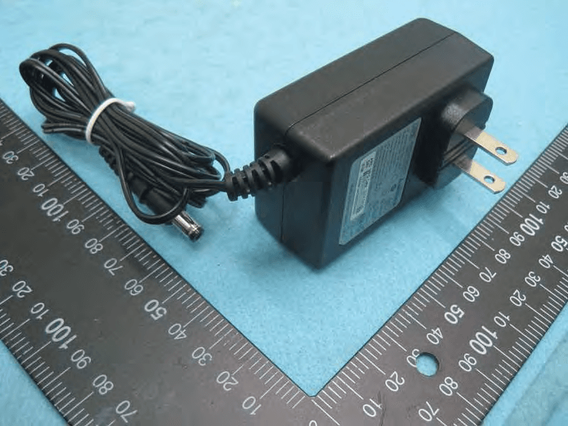
FDI000000028
Mar 15, 2015AirStation
Equipment Class
DTS - Digital Transmission System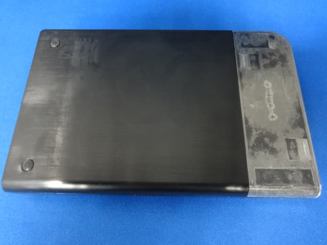
FDI000000027
Jan 22, 2015MiniStation
Equipment Class
DXX - Part 15 Low Power Communication Device Transmitter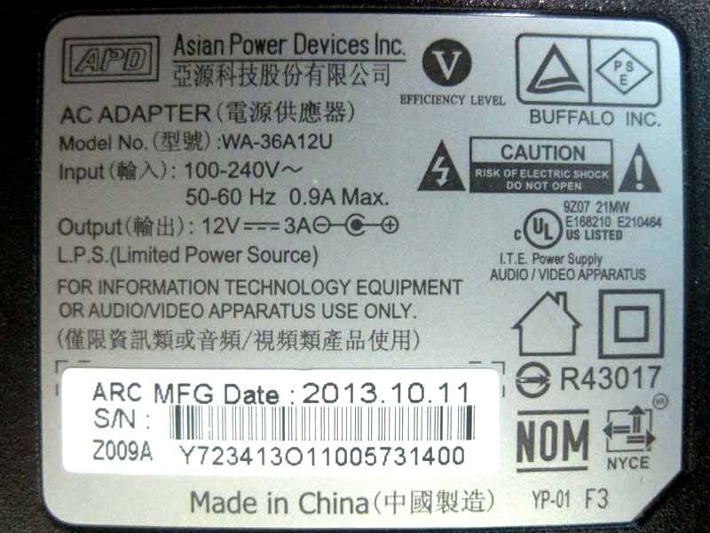
FDI000000022
Oct 12, 2014AirStation
Equipment Class
DTS - Digital Transmission System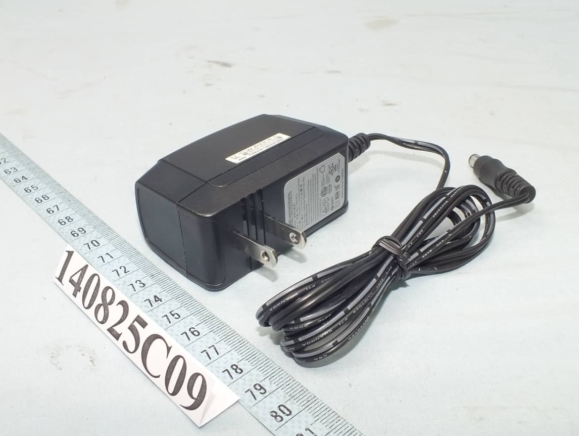
FDI000000026
Oct 01, 2014AirStation
Equipment Class
DTS - Digital Transmission System
FDI000000024
Apr 21, 2014AirStation
Equipment Class
DTS - Digital Transmission System