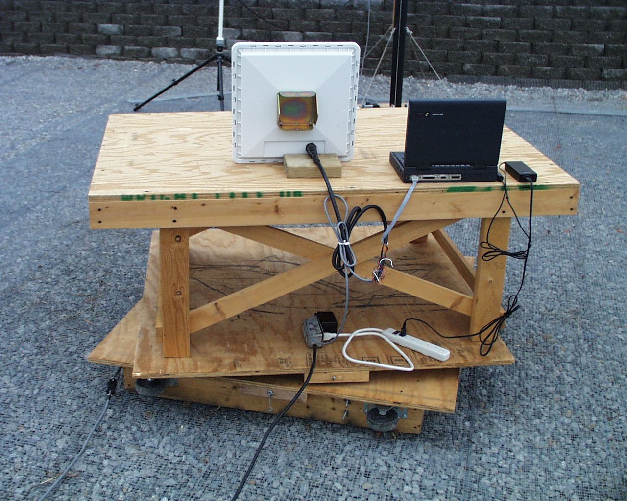
FIH10-510-100Location and Monitoring Transmitter
TransCore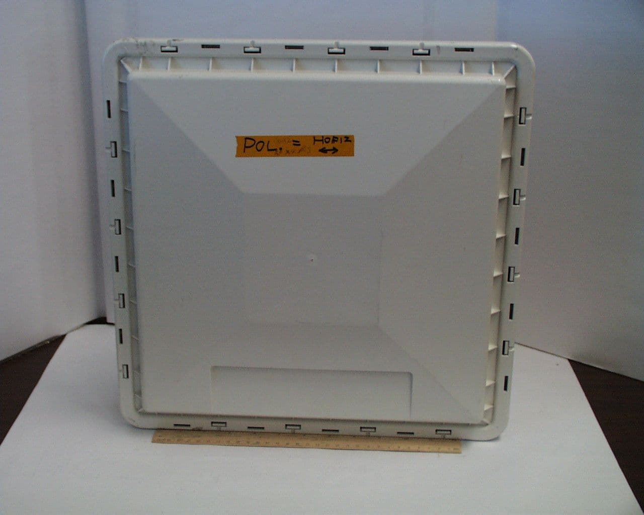
Click to zoom
Application Details
- Equipment Class
- LMS - Part 90 Location & Monitoring Transmitter
- Date of Grant
- Feb 17, 2000
- Application Purpose
- Original Equipment
- Date of Application
- Dec 09, 1999
- Equipment Note
- Location and Monitoring Transmitter
- Frequency Range
- 912.50000000 - 919.00000000
- Company
- TransCore
- Country
- United States
Documents & Files
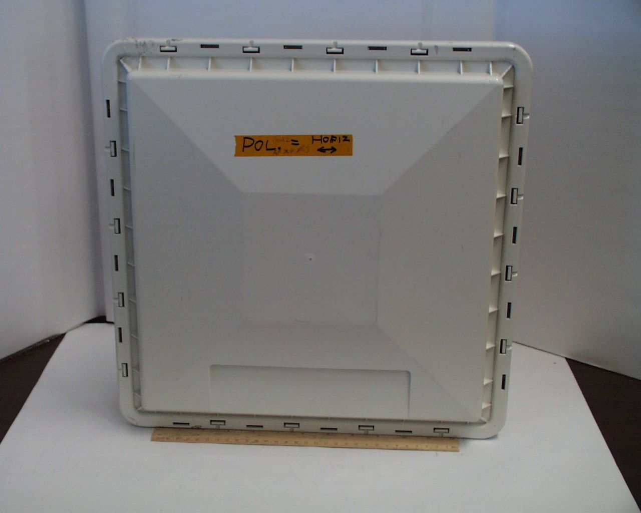
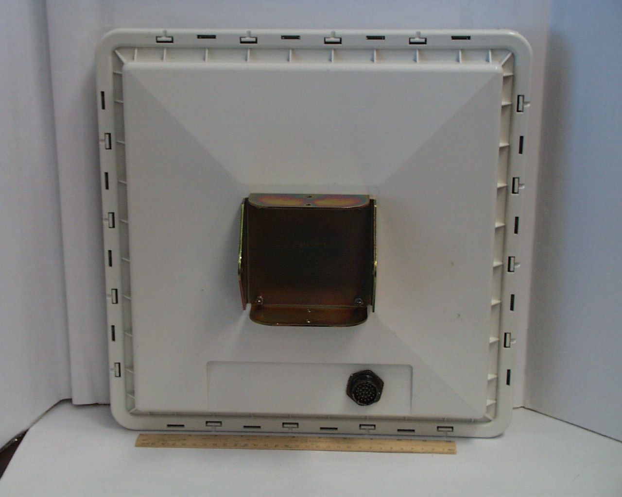
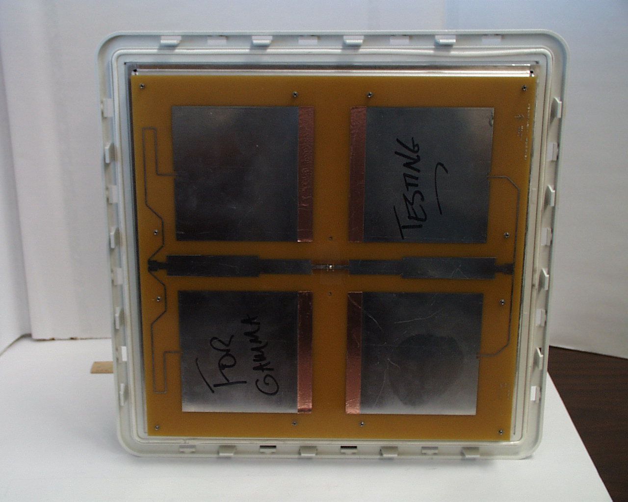
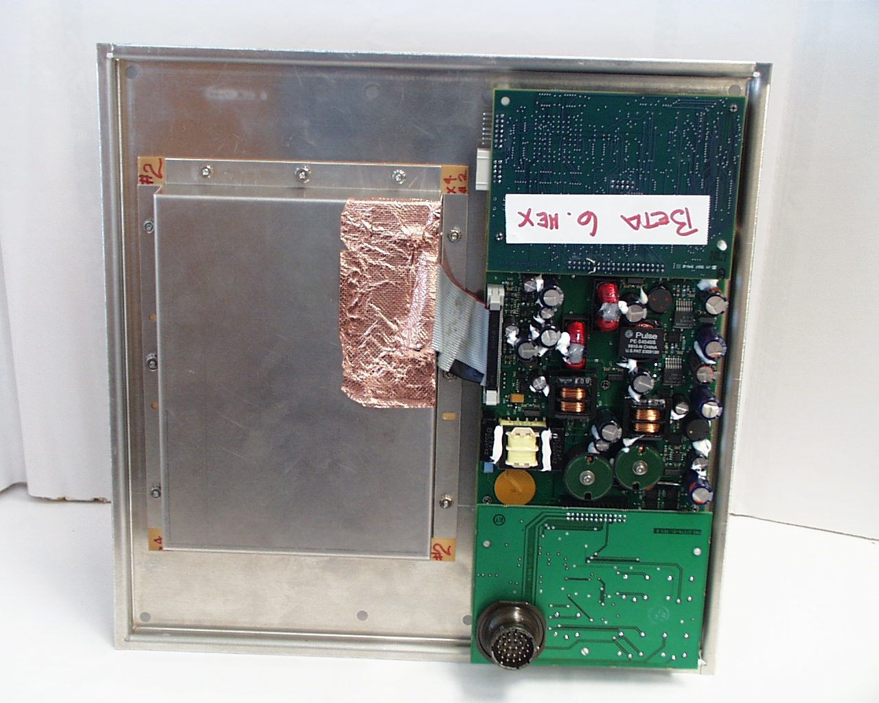
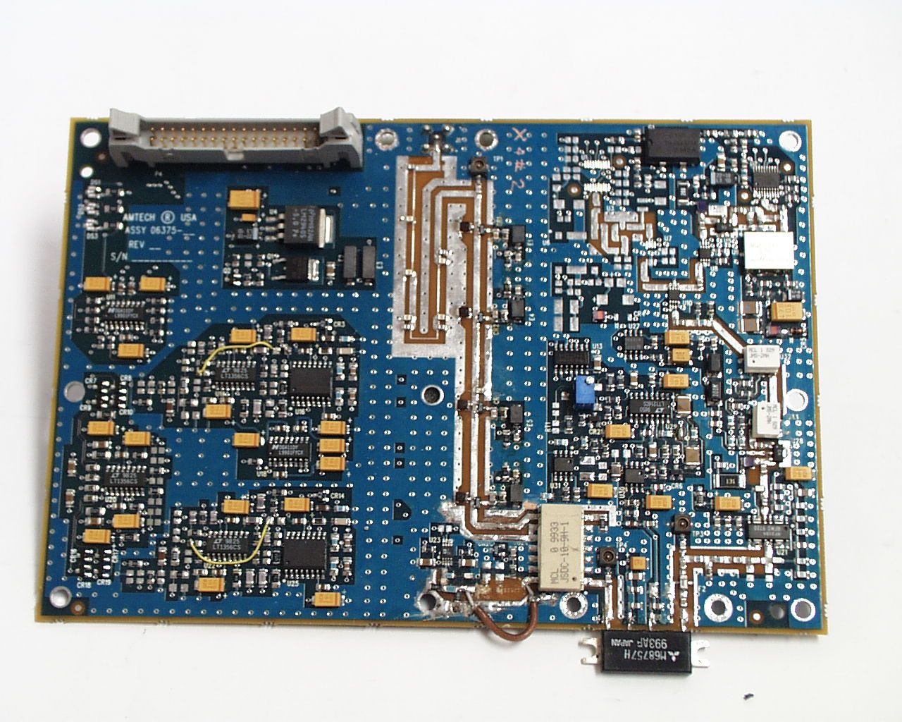
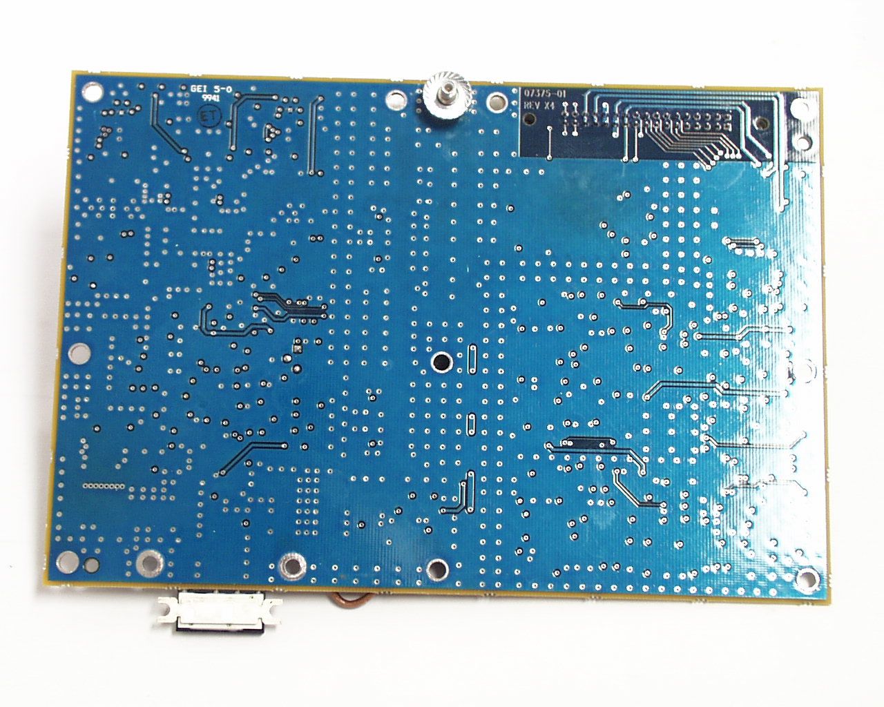
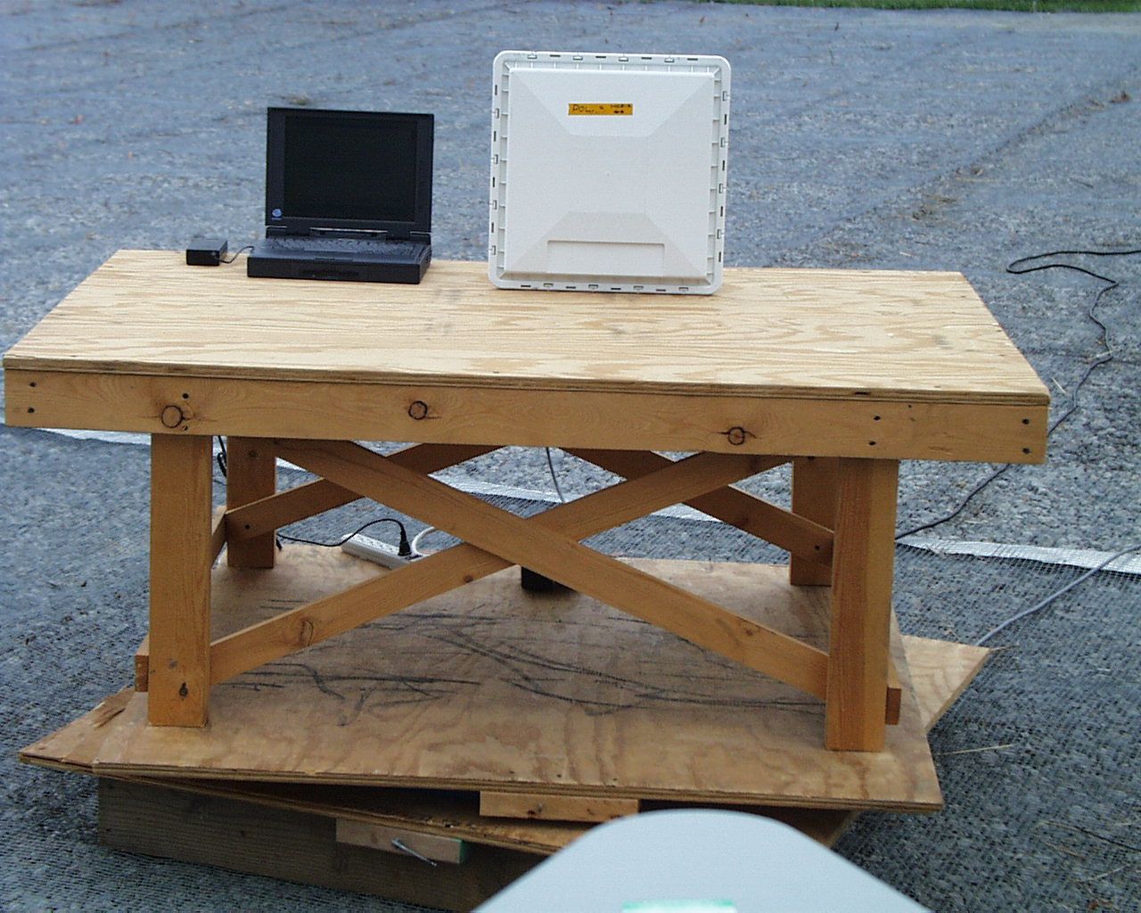
Document Text
Text extracted from the exhibit documents filed with the FCC. Open a document above to read the original.
Users Manual
P/N 411288-002 System Guide AI1620 SmartPass ® Information in this document is subject to change and does not represent a commitment on the part of Amtech Systems Corporation. © 1999 Amtech Systems Corporation. (Amtech Systems Corporation is a wholly owned subsidiary of Intermec Technologies Corporation.) All rights reserved. No portion of this publication may be reproduced or transmitted in any form by any means without prior written permission of Amtech Corporation. Aspects of the wireless data and security equipment and systems marketed by Amtech Systems Corporation and its affiliates are protected by patents and patents pending in the United States and other countries. Amtech is a registered trademark of Amtech Systems Corporation. SmartPass ® is a registered trademark of Amtech Systems Corporation. Throughout this manual, trademarked names may be used. Rather than put a trademark symbol (™ or ® ) in every occurrence of a trademarked name, we state that we are using the names only in an editorial fashion and to the benefit of the trademark owner, with no intention of infringement. All other trademarks listed are the property of their respective owners. Printed in the U.S.A. For further information, contact: Amtech Systems Corporation 19111 Dallas Parkway, Suite 300 Dallas, Texas 75287-3106 USA Phone:(972) 733-6600 Fax:(972) 733-6699 Amtech Response Center 19111 Dallas Parkway, Suite 300 Dallas, Texas 75287-3106 USA Phone:(972) 733-6681 Fax:(972) 733-6695 WARNING TO USERS IN THE UNITED STATES FEDERAL COMMUNICATIONS COMMISSION (FCC) RADIO FREQUENCY INTERFERENCE STATEMENT 47 CFR §15.105(a) NOTE: This equipment has been tested and found to comply with the limits for a Class A digital device pursuant to Part 15 of the Federal Communications Commission (FCC) rules. These limits are designed to provide reasonable protection against harmful interference when the equipment is operated in a commercial environment. This equipment generates, uses, and can radiate radio frequency (RF) energy and may cause harmful interference to radio communications if not installed and used in accordance with the instruction manual. Operating this equipment in a residential area is likely to cause harmful interference, in which case, depending on the laws in effect, the users may be required to correct the interference at their own expense. NO UNAUTHORIZED MODIFICATIONS 47 CFR §15.21 CAUTION: This equipment may not be modified, altered, or changed in any way without permission from Amtech Corporation. Unauthorized modification may void the equipment authorization from the FCC and will void the Amtech warranty. USE OF SHIELDED CABLES IS REQUIRED 47 CFR §15.27(a) Shielded cables must be used with this equipment to comply with FCC regulations. A license issued by the FCC is required to operate this RF identification device in the United States. Contact Amtech Corporation for additional information concerning licensing requirements for specific devices. Amtech Corporation USA Contents Table of Contents vii Table of Contents Introduction Introduction 1-3 Audience 1-3 System Guide Organization 1-3 Document Conventions 1-4 System Description 1-4 License Requirements 1-5 Developing the Site Plan Overview 2-3 Reader and Tag Alignment 2-3 Polarization 2-4 Unobstructed Line of Sight 2-5 Site Layout and Traffic Flow 2-7 SmartPass Read Zone 2-8 Other SmartPasses in the Area 2-8 Lane Configurations 2-8 Open Lane Configuration 2-8 Gate with Center Island Configuration 2-11 Parking Garage with Ticket Island Configuration 2-11 Reflection, Refraction, and Diffraction of RF Signals 2-12 Existing Interference 2-13 Electrical and Communications Requirements 2-13 Junction Box 2-13 Power and Communications Cable 2-13 Electrical Power 2-14 Host Communications 2-15 RS–232 Interface 2-16 RS–422 Interface 2-16 Wiegand Interface 2-16 Input/Output Circuits 2-16 1 2 AI1620 SmartPass System Guide viii Choosing, Installing, and Removing Tags Tag Types 3-3 Tag Models 3-3 Reader/Tag Interoperability 3-5 Tag Data Formats 3-6 Installing Interior Tags 3-6 Materials Required 3-7 Tag Positioning 3-7 Interior Driver’s or Passenger’s Side 3-7 Interior Center Windshield 3-8 Installation Procedures 3-8 Removing Interior Tags 3-9 Installing Exterior Tags 3-9 Materials Required 3-10 Tag Positioning 3-10 Installation Procedures Using Tape 3-11 Installation Procedures Using Blind Rivets 3-11 Removing Exterior Tags 3-11 Testing and Configuring SmartPass Before Installation Materials Required 4-3 Materials Supplied 4-3 Cable Supplied 4-3 Additional Materials Needed 4-4 Testing Using an Audible Circuit Tester 4-4 Connecting the AC Power Supply 4-5 Connecting the DC Power Supply 4-6 Testing SmartPass 4-6 Configuring SmartPass 4-7 Connecting SmartPass to the PC 4-7 Using a RS-232 Interface 4-7 Using RS-422 Interface 4-10 Using Wiegand Interface 4-10 Default Configuration Settings 4-12 General Configuration Settings 4-12 Operating Parameter Settings 4-12 Configuring Operating Parameters Using Terminal Emulation Software 4-14 3 4 Table of Contents ix Configuring Operating Parameters Using SmartPass Host 4-14 Loading and Starting SmartPass Host 4-15 Verifying PC-to-SmartPass Communications 4-15 Verifying Tag Read Capability 4-18 Configuring SmartPass Parameters 4-20 Reset 4-25 General Software Information Command Entry Conventions 5-3 Command Response Conventions 5-4 Operating Parameters 5-5 Power Fail 5-5 Program Download 5-5 Download Considerations 5-5 Download Procedures 5-6 Startup 5-7 Sign-On Message 5-7 Boot Failure Message 5-7 Tag/Message Buffer 5-7 Communication Protocols Introduction 6-3 Basic Protocol 6-3 Error Correcting Protocol 6-4 Data Inquiry Protocol 6-4 Basic and ECP Protocol Format 6-5 Reader Transmissions 6-5 ECP Host ACK/NAK Response 6-6 Switch to Command Mode Request 6-7 Host Transmission 6-7 Reader Command Response 6-8 Sample Messages 6-9 Reader Transmissions 6-9 Host Command Transmissions 6-9 5 6 AI1620 SmartPass System Guide x Timing and Sync…
Text truncated - open the document above for the full version.
Users Manual
F Intellitag ® 500 SmartPass ® Reader System Modifications Intellitag® 500 SmartPass® Reader System Modifications F-3 F This appendix describes the changes made to the AI1620 SmartPass ® Reader to make the system guide usable for the Intellitag ® 500 SmartPass Reader system. Introduction This addendum to the AI1620 SmartPass® System Guide provides information about hardware and software modifications for the Intellitag 500 SmartPass Reader system. Audience This document is intended to be used by authorized SmartPass dealers, installers, and service personnel. Because SmartPass has no operator- or end-user-serviceable components or features, no end-user manual or operator guide exists. Once the system is set up and tested by the authorized installer, SmartPass operations requires no end- user intervention. Reader Modifications The following sections describe the proposed modification and reason for each of the Intellitag 500 SmartPass Reader system changes. Each section lists the modification, the background of the reason for the change (if provided), and the firmware commands affected by the change (if applicable). Reading of Mixed Population Tags Modification The Intellitag 500 SmartPass Reader reads the American Trucking Association (ATA) or International Organization for Standardization (ISO) read-only type tags, whether battery or beam powered, or Intellitag 500 asynchronous integrated circuit (ASIC)- based tags. The reader can read the ATA or ISO read-only tags in the presence of Intellitag 500-based tags; however, attempting to read a Intellitag 500-based tag in the presence of an ATA or ISO read-only tag might provide indeterminate results. At present, Amtech is aware that the performance under these conditions is strongly determined by physical and geometrical factors. Background The traditional Amtech read-only tags are continuously modulating regardless of the state of the reader or Intellitag 500 tags. Therefore, when a polling request signal is sent from the reader to the Intellitag 500 tags, it is probable that the read-only tags can interfere with the backscatter response from the Intellitag 500 tag. This creates Intellitag® 500 SmartPass® Reader System Modifications F-4 difficulty for the reader in reading the response from the Intellitag 500 tag, or can cause the reader to miss the response from the Intellitag 500 tag altogether. The Intellitag 500 SmartPass Reader system can read either a read-only ATA or ISO type tag, or a Intellitag 500 tag in a given vehicle, but not both simultaneously. If a vehicle is equipped with both tag types, it is probable that the read-only tag will be read; however, it is very possible that the Intellitag 500 tag will not be read, depending on a number of factors. The factors that influence the readability include, but are not limited to, physical orientation and configuration; the type of read-only tag; the ratio of backscatter cross-section of the tags; and whether the tag is battery or beam powered. Commands No direct impact on commands. Programmable Attenuation Control Added Modification Replacing the range control function gives the Intellitag 500 SmartPass Reader a programmable attenuation control for the output radio frequency (RF) power. This feature simplifies the design and streamlines the testing during manufacturing and installation processes. Valid settings for attenuation are in 1.0 dB increments over a range of 10-dB attenuation, from the maximum power setting of 2 watts at 0-dB attenuation to a minimum power level of 200 milliwatts at 10-dB attenuation. Commands This modification introduces the following command: 644NNSet RF attenuation (new command) Table F-1 lists the Set RF attenuation command variable (NN) and attenuation settings. Table F-1 Set RF Attenuation Command Settings and Variables Variable (NN) Attenuation Setting (dB) 000 011 022 033 044 055 Intellitag® 500 SmartPass® Reader System Modifications F-5 F Real-Time Clock, Time/Date Stamping Removed Modification The Intellitag 500 SmartPass Reader design eliminates the real-time clock, thereby eliminating all functions associated with setting the time and date. This change reduces the recurring cost of the reader, and might alleviate concerns associated with maintenance, environmental, and shipping issues because the battery is being eliminated. The reader responds to set time and date commands with an error message, except for the Disable time/date append command. For this command, the Intellitag 500 SmartPass Reader responds with Done. Commands This modification affects the following commands: 20S...SSet time 21S...SSet date 22Display time and date 300Disable time and date append 302Enable time and date append 524Display appended info status 661Display diagnostics results 664Test real-time clock Tag Data Buffering and Storage Reduced Modification The Intellitag 500 SmartPass Reader does not provide tag memory storage beyond the quantity required for data buffering from the tag to the host. The Intellitag 500 SmartPass Reader responds with an error message to commands associated with this function, except for the Disable buffer control mode when a Done response is returned. 066 077 088 099 0A10 Table F-1 Set RF Attenuation Command Settings and Variables Intellitag® 500 SmartPass® Reader System Modifications F-6 Commands This modification affects the following commands: 06Transmit buffer entry 43Buffer all IDs 530Display RF0 filter status 535Display buffer control status 613Select data inquiry protocol 6160Disable buffer control mode 6161Enable buffer control mode Check Tag Function Removed Modification The Intellitag 500 SmartPass Reader design eliminates the Self-test Check Tag function. The reader responds with an error message to all commands associated with this function, except for Disable periodic check tag when the reader returns a Done response. Additional alternate diagnostics functions may be investigated for feasibility to integrate into the reader. Comm…
Text truncated - open the document above for the full version.
Cover Letter(s)
Request for Confidential Treatment - Intermec Technologies Corp., Amtech Services Division FCC ID No: FIH 10-510-100 Intermec Technologies Corp. requests that the materials in Exhibits 4 (Block Diagram), 5 (Schematics) and 6 (Parts List) be withheld from public disclosure in accordance with Section 0.459 of the Commission’s Rules, 47 C.F.R. § 0.459 (1998), following grant of the application. In support of this request, Intermec submits the following: (1) identification of the specific information for which confidential treatment is sought: The materials set forth in the Block Diagram, Schematics and Parts List exhibits, which are segregated from the non-confidential exhibits of the application, are those for which confidentiality is sought. (2) identification of the Commission proceeding in which the information was submitted or a description of the circumstances giving rise to the submission: The proceeding is that involving the application for equipment authorization (certification) under FCC ID No.: FIH 10-510-100 (3) explanation of the degree to which the information is commercial or financial, or contains a trade secret or is privileged: This material includes circuit diagrams (schematics and blocks) and lists of parts that make up the transmitter. As such, this material is treated as highly confidential business information. (4) explanation of the degree to which the information concerns a service that is subject to competition: The material for which confidentiality is sought is employed in the design and manufacture of Location and Monitoring Service transmitting equipment that is offered on a highly competitive basis. Customers for this equipment have a variety of competing sources of supply. (5) explanation of how disclosure of the information could result in substantial competitive harm: Disclosure would, in effect, give away the fruits of the labors of Intermec’s engineering personnel, who have designed the equipment and the manufacturing processes. Disclosure would also offer competitors additional unwarranted insight into the state of product development thereby allowing such competitors an advantage that would not be available to Intermec. (6) identification of any measures taken by the submitting party to prevent unauthorized disclosure: The information for which confidential treatment is sought is kept confidential by Intermec and not made available to third parties except pursuant to non-disclosure agreements. (7) identification of whether the information is available to the public and the extent of any previous disclosure of the information to third parties: To the knowledge of those preparing this application, the information has not been disclosed publicly heretofore. While the general theory of operation of this non-multilateration equipment has been the subject of numerous disclosures in industry and standards groups as well as in rule making proceedings at the FCC, the protection sought is narrowly drawn and pertains to certain specific implementations of modulated backscatter radio technology. (8) justification of the period during which the submitting party asserts that material should not be available for public disclosure: This material should not be disclosed for at least 25 years. While improvements in design are made relatively frequently, disclosure of the design information would lead to insights into both designs and manufacturing techniques and could have an adverse competitive effect for many years to come. This equipment is designed for commercial, industrial, and governmental transportation applications. As such, unlike most consumer equipment, it is expected to be used for more than a decade in some cases. Moreover, this equipment will be used in revenue collection (e.g. toll collections) and secure access control applications (e.g. freight handling facilities). As such, it is important that its design not be made available to unauthorized persons who might attempt to use knowledge of the design to compromise the applications for which the equipment will be employed. (9) any other information that the party seeking confidential treatment believes may be useful in assessing whether its request for confidentiality should be granted: See item 8 above. Note that the equipment for which approval is being sought will be employed in applications that inherently carry a premium on security. Sincerely, ________/s/_____________ Wesley M. Mays Manager, Microwave Design
Operational Description
FUNCTION OF EACH ACTIVE CIRCUIT DEVICE Referring to the PARC Reader RF Module Schematic, 10405, page 2, U2 is a frequency synthesizer chip that operates in conjunction with U9, a voltage controlled oscillator (VCO). These form the primary frequency source. Provisions have been made for an alternate frequency source that would be formed by U1 and U6, but these parts are not installed or used in the PARC Reader. They are labeled as “NO LOAD” on the schematic. Amplifier U5 serves to amplify the VCO signal and switches U8, U10 and U7 would serve to switch between the primary and the (unused) alternate frequency source with a large amount of isolation. Switch U7 is not installed and switches U8 and U10 are always set to select the primary source. On page 3, the signal path for the transmitter continues. U32 and U33 are passive double- balanced mixers configured as an amplitude modulator with an ON/OFF ratio of more than 40 dB. U27 provides the data modulating signal through a filter to the intermediate frequency (IF) ports of the mixers. An amplifier, U28, follows the modulator. The output signal from U28 is applied to the transmit driver stage, U21. The driver signal is filtered by F2 and applied to the transmit power amplifier (PA), U26. The PA output passes through a directional coupler, U24, which develops a reduced amplitude, coupled signal for the power control function, discussed later. From the PA, the transmit signal passes through the homodyne on page 5, to a harmonic filter and on to the antenna. In the homodyne, there are two signals moving in opposite directions: the transmit signal to the antenna and the receive signal from the antenna to the homodyne. The transmit signal also acts as a local oscillator for the nonlinear mixer diodes CR15, CR11, CR2 and CR1 to provide conversion of the incoming receive signal from the antenna to the baseband in-phase (I) and quadrature (Q) differential signals, which are applied to the receiver preamp. The baseband I and Q preamp is shown on pages 6 and 7. The amplified I-Data and Q-Data from page 7 is provided to the PARC Processor Module via pins 7 and 8 of connector P4 on page 1. The power control circuit works as follows, referring to page 4. U23 is a logarithmic detector/controller. The power level from the directional coupler following the PA, U24 on page 3, is attenuated and applied to pins 2 and 3 of U23. The power level control or reference signal is applied to pin 7 of U23. This reference signal is developed from a D/A converter on the Processor Module, which provides a RF ATTEN signal on pin 6 of connector P4 (page 1). An RF ATTEN voltage of approximately 2.5 volts DC corresponds to a full power output of 2 watts. The voltage divider formed by R154, R166, R182, R190 and R165 precisely adjusts the reference voltage for a full power output of 2 watts. Capability is provided to decrease power up to 10 dB in one dB steps by varying the RF ATTEN signal under software control. A detected power level indication is provided to the Processor Module by CR20 and U30 on page 3. The output of the log detector/controller IC, U23, is buffered and filtered by U30 and U31 and applied to the power control input at pin 2 of U26, the PA device.
Parts List/Tune Up Info
Revised 12/3/99 TUNEUP PROCEDURE At full power level of 2 watts, the resistive voltage divider formed by R154, R166, R182, R190 and R165 determines the reference voltage, VSET, that is applied to the logarithmic detector/controller, U23. U23 provides the power control voltage, VCONTROL, that is applied to the transmit power amplifier, U26. This is a closed loop power control system that does not require external adjustments. The Processor can also select a power of less than 2 watts, via the RF ATTEN signal, in power reduction steps of about 1 dB down to -10 dB. FREQUENCY STABILIZING CIRCUITRY The frequency source is shown on page two of the RF Module schematic 10405. U2 is a frequency synthesizer chip, which in conjunction with the voltage controlled oscillator (VCO), U9, provides a frequency output of 912.5 to 919.0 MHz in steps of 500 kHz, resulting in 14 channels. The reference oscillator, G1, provides a stable 16 MHz signal to the synthesizer chip at U2 pin 8. The 16 Mhz reference signal is divided down by a factor of 32 to 500 kHz internally within U2. This sets the frequency spacing between channels to 500 kHz. The 16 Mhz reference oscillator, G1, has a frequency stability of + or – 200 ppm, which determines the basic frequency stability of the transmitter. SPURIOUS SUPPRESSION, MODULATION LIMITING AND POWER LIMITING Spurious products and harmonics in the transmitter are attenuated by the filter F1 on page 3 of RF Module schematic 10405 and the filter on page 5 formed by Z28 through Z33and C39, C40, C65, C73, C72, C67, C46, C30 and C8. A plot of the measured frequency response of the filter is shown in the attached Figure 1. The data modulator is on page 3 of schematic 10405. This modulator, formed by U32, U33, U27 and the lowpass filter following U27, achieves 100% amplitude modulation with an ON/OFF ratio of more than 40 dB. The filter following U27 provides shaping of the incoming data in order to limit the bandwidth of the modulated signal to less than 5 Mhz, typically 3 MHz, at 58 dB down. Full power limiting is accomplished using a logarithmic detector/controller IC, U23, on page 4. U23 produces an output voltage proportional to the difference of the logarithm of the incoming signal, RF POWER, on pins 2 and 3 and the DC power set level, VSET, applied to pin 7 of U23. The signal on pin 3, RF POWER, is a sample of the transmitted signal obtained from the directional coupler, U24, and suitably attenuated by R150, R151, and R153 and R196, R198 and R199. The output of the logarithmic detector/controller on pin 8 of U23 is buffered and filtered by U31 and U30 and applied to the power control terminal, pin 2 of U26, of the power amp (PA) on page 3 of the schematic. Nominally, 2.5 volts DC at pin 2 results in a full power of two watts to the antenna. The resistive voltage divider network formed by R154, R166, R182, R190 and R165 results in a precise adjustment of VSET, for 2 watts output at full power. DESCRIPTION OF DIGITAL MODULATOR The digital data modulator is shown on page 3 of the RF Module schematic 10405 and is formed by U32, U33, U27 and the lowpass filter at the output of U27. This is an amplitude modulator which achieves an ON/OFF ratio in excess of 40 dB. The response for the filter realized with L13 through L15, C225 through C227 and C198 is attached as Figure 2. This filter achieves a rejection of about 58 dB at the 1.5MHz point resulting in a modulated bandwidth of about 3 MHz at 58 dBc when excited with 30 KB/s data modulation. The modulation is at 30 KB/s and consists of 22 synchronization bits followed by a 1 ms. pause and then approximately 216 more bits. The pattern is retransmitted approximately every 11 ms. with a pause of about 6 ms. between 5 ms. bursts. During all pauses, the carrier is on continuously without modulation. During the 6ms. pause, the PARC Reader receives reflected modulated carrier back from the target RF tag(s).
Test Report
Test Report For Application of Certification For INTERMEC TECHNOLOGIES CORPORATION AMTECH SYSTEMS DIVISION 8600 Jefferson Street, NE Albuquerque, NM 87113 Phone: (505) 856-8054 MODEL: Parking Access and Revenue Collection (PARC) Reader 10-510-100 LMS Transmitter FREQUENCY: 912.5-919 MHz FCC ID: FIH 10-510-100 Test Date: November 29, 1999 Certifying Engineer: Scot D. Rogers ROGERS LABS, INC. 4405 W. 259th Terrace Louisburg, KS 66053 Phone: (913) 837-3214 FAX: (913) 837-3214 This report shall not be reproduced except in full, without the written approval of the laboratory. This report must not be used by the client to claim product endorsement by NVLAP or any agency of the U.S. Government. NVLAP Accredited LaboratoryNVLAP Lab Code: 200087-0 ROGERS LABS, INC.INTERMEC TECHNOLOGIES CORPORATION AMTECH SYSTEMS DIVISION 4405 W. 259th TerraceMODEL: 10-510-100 Parking Access and Revenue Collection PARC Louisburg, KS 66053Test #: 991119FCC ID#: FIH 10-510-100 Phone/Fax: (913) 837-3214Test to: FCC Parts 2 and 90Page 2 of 25 Certification\AMTPARC.DOC November 29, 1999 TABLE OF CONTENTS FORWARD:3 LIST OF TEST EQUIPMENT3 2.1033(C)APPLICATION FOR CERTIFICATION4 2.1046RF POWER OUTPUT5 Measurements Required:5 Test Arrangement:5 Results:5 2.1047MODULATION CHARACTERISTICS8 Measurements Required:8 Test Arrangement:8 Results:8 2.1049OCCUPIED BANDWIDTH8 Measurements Required:8 Test Arrangement:9 Results:9 2.1051SPURIOUS EMISSIONS AT ANTENNA TERMINALS10 Measurements Required:10 Test Arrangement:10 Results:12 2.1053FIELD STRENGTH OF SPURIOUS RADIATION12 Measurements Required:12 Test Arrangement:12 Radiated (8 Highest Emissions)14 Results:14 2.1055FREQUENCY STABILITY15 Measurements Required:15 Test Arrangement:15 Results:16 APPENDIX17 NVLAP Accredited LaboratoryNVLAP Lab Code: 200087-0 ROGERS LABS, INC.INTERMEC TECHNOLOGIES CORPORATION AMTECH SYSTEMS DIVISION 4405 W. 259th TerraceMODEL: 10-510-100 Parking Access and Revenue Collection PARC Louisburg, KS 66053Test #: 991119FCC ID#: FIH 10-510-100 Phone/Fax: (913) 837-3214Test to: FCC Parts 2 and 90Page 3 of 25 Certification\AMTPARC.DOC November 29, 1999 FORWARD: In accordance with the Federal Communications Code of Federal Regulations, dated October 1, 1998, Part 2 Subpart J, Paragraphs 2.907, 2.911, 2.913, 2.925, 2.926, 2.1031 through 2.1057; 90.201 through 90.217, 90.350 through 90.363; and Report and Order FCC 98-58 the following is submitted: List of Test Equipment A Hewlett Packard 8591EM and or 8562A Spectrum Analyzer was used as the measuring device for the emissions testing. The analyzer settings used are described in the following table. Refer to Appendix for a complete list of Test Equipment. HP 8591EM SPECTRUM ANALYZER SETTINGS CONDUCTED EMISSIONS: RBWAVG. BW DETECTOR FUNCTION 9 kHz30 kHzPeak/Quasi Peak RADIATED EMISSIONS (30 - 1000 MHz): RBWAVG. BW DETECTOR FUNCTION 120 kHz300 kHzPeak/Quasi Peak HP 8562A SPECTRUM ANALYZER SETTINGS RADIATED EMISSIONS (1 - 40 GHz): RBWAVG. BW DETECTOR FUNCTION 1 MHz1 MHzPeak/Average ANTENNA CONDUCTED EMISSIONS: RBWAVG. BW DETECTOR FUNCTION 100 kHz300 kHzPeak NVLAP Accredited LaboratoryNVLAP Lab Code: 200087-0 ROGERS LABS, INC.INTERMEC TECHNOLOGIES CORPORATION AMTECH SYSTEMS DIVISION 4405 W. 259th TerraceMODEL: 10-510-100 Parking Access and Revenue Collection PARC Louisburg, KS 66053Test #: 991119FCC ID#: FIH 10-510-100 Phone/Fax: (913) 837-3214Test to: FCC Parts 2 and 90Page 4 of 25 Certification\AMTPARC.DOC November 29, 1999 2.1033(c)Application for Certification 1.Manufacturer:INTERMEC TECHNOLOGIES CORPORATION Amtech Systems Division 8600 Jefferson Street, NE Albuquerque, NM 87113 2.Identification:Model:10-510-100 FCC I.D.: FIH 10-510-100 3.Refer to Installation and Operating Instruction Manual. 4.Emission Type: Continuous Wave Emission Designator. NON Modulated Signal Emission Designator. 220kL1D 5.Frequency Range: 912.5 – 919.0 MHz 6.Operating Power Level: 2 Watts. Maximum power output is factory set and may be attenuated up to 10 dB in 1-dB steps via software. 7.Max P o : 2 Watts per channel. 8.Power into final amplifier: +8.5 Vdc @ 0.8 amps (6.8 Watts) 9.Tune Up Procedure: Refer to Exhibits. 10. Refer to Exhibits for function of semiconductors and other active devices. 11. Refer to Exhibit for FCC ID Label. 12. Refer to Exhibit for photographs of equipment. 13. Refer to Exhibit for details of modulation techniques. NVLAP Accredited LaboratoryNVLAP Lab Code: 200087-0 ROGERS LABS, INC.INTERMEC TECHNOLOGIES CORPORATION AMTECH SYSTEMS DIVISION 4405 W. 259th TerraceMODEL: 10-510-100 Parking Access and Revenue Collection PARC Louisburg, KS 66053Test #: 991119FCC ID#: FIH 10-510-100 Phone/Fax: (913) 837-3214Test to: FCC Parts 2 and 90Page 5 of 25 Certification\AMTPARC.DOC November 29, 1999 2.1046RF Power Output Measurements Required: Measurements shall be made to establish the radio frequency power delivered by the transmitter into the standard output termination. The power output shall be monitored and recorded and no adjustment shall be made to the transmitter after the test has begun, except as noted below: If the power output is adjustable, measurements shall be made for the highest and lowest power levels. Test Arrangement: The radio frequency power output was measured at the antenna terminals by replacing the antenna with a spectrum analyzer, 20dB Attenuator and cable (with 2dB loss in the cable). The spectrum analyzer had impedance of 50Ω to match the impedance of the standard antenna. A HP 8591EM Spectrum Analyzer was used to measure the radio frequency power at the antenna port. The data was taken in dBm and converted to watts as shown in the following Table. Refer to Figures 1 through 3 showing the output power of the transmitter. Data taken per Paragraph 2.1046(a) and applicable parts of Part 90. P dBm = power in dB above 1 milliwatt. Milliwatts = 10 (PdBm/10) Watts = (Milliwatts)(0.001)(W/mW) Results: 0 dB ATTENUATION FREQUENCYP dBm P mw P w 912.033.01,9952.0 916.033.01,9952.0 919.032.81,9052.0 TRANSMITTER SPE…
Text truncated - open the document above for the full version.
Contact Information
Applicant
Dale Scott(VP of Engineering and Manufacturing)
Technical Contact
Amtech Systems Division, Intermec TechnologiesWes Mays
[email protected]505-856-8054
8600 Jefferson St, NE · Albuquerque, New Mexico · United States
Non-Technical Contact
Wiley, Rein & FieldingDavid E Hilliard
[email protected]202-719-7058
Test Firm
Rogers Labs, Inc.Scot Rogers
Technical Specifications
| # | Rule Parts | Frequency Range | Power Output | Emission | Tolerance |
|---|---|---|---|---|---|
| 2 | 90.353 | 912.5 MHz - 919 MHz | 2 W | 220KL1D | 25 ppm |
Other Applications from TransCore
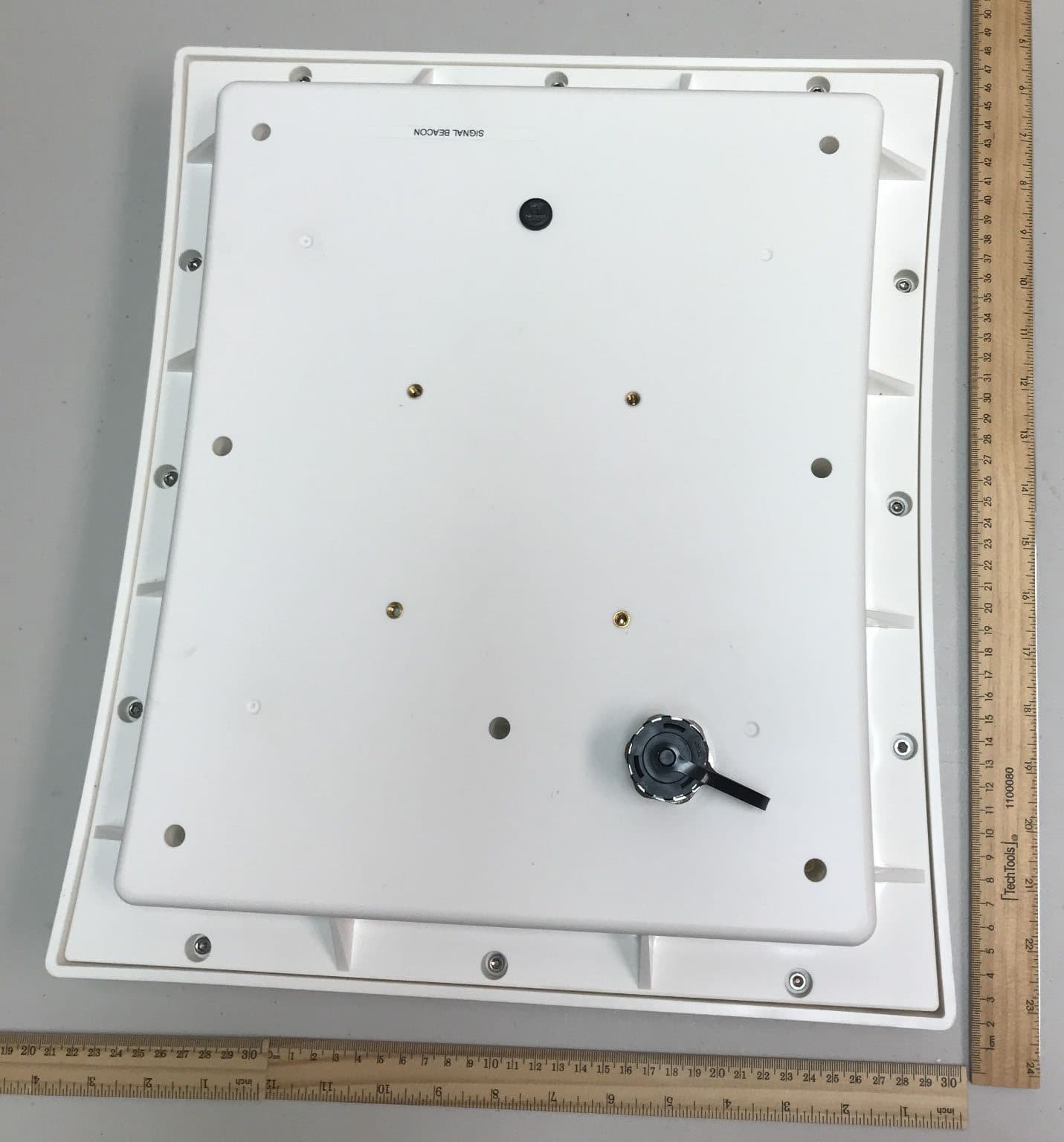
FIHSPSBPT15V1
Aug 27, 2026Low Power Communication Device for use in Toll exchange applications
Equipment Class
DTS - Digital Transmission System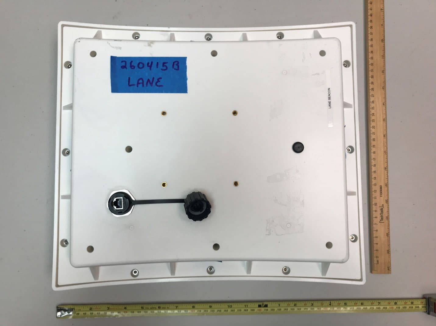
FIHSPLBPT15V1
Aug 26, 2026Low Power Communication Device for use in Toll exchange applications
Equipment Class
DTS - Digital Transmission System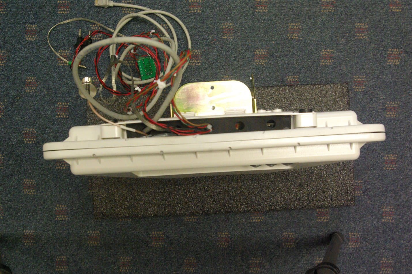
FIHE4FPT90V1
Sep 04, 2023Location and Monitoring Service Interrogator
Equipment Class
TNB - Licensed Non-Broadcast Station Transmitter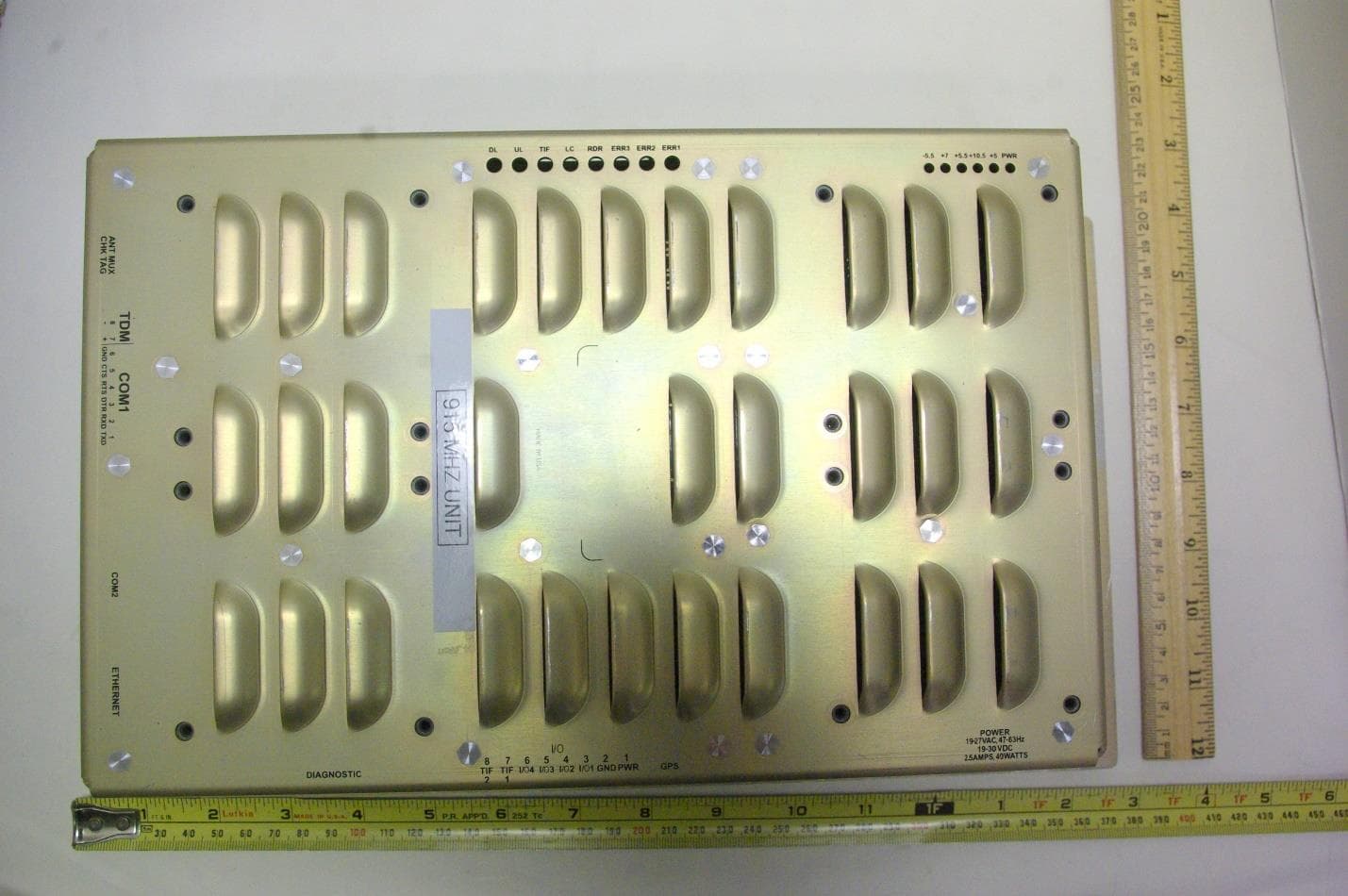
FIHE6PT90V2
Jan 24, 2023Location and Monitoring Service Interrogator
Equipment Class
TNB - Licensed Non-Broadcast Station TransmitterFIHE4SPT90V5
Jun 02, 2022Location and Monitoring Service Interrogator
Equipment Class
TNB - Licensed Non-Broadcast Station Transmitter