GKRWM3B0B32Notebook With 2.4GHz Wireless LAN Module
Compal Electronics Inc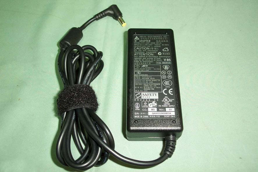
Click to zoom
Application Details
- Equipment Class
- DTS - Digital Transmission System
- Date of Grant
- Sep 29, 2003
- Application Purpose
- Original Equipment
- Date of Application
- Sep 29, 2003
- Equipment Note
- Notebook With 2.4GHz Wireless LAN Module
- Frequency Range
- 2412.00000000 - 2462.00000000
- Company
- Compal Electronics Inc
- Country
- Taiwan
Documents & Files
Document Text
Text extracted from the exhibit documents filed with the FCC. Open a document above to read the original.
Users Manual
CL32 User Manual Safety Instructions Use the following safety guidelines to help protect yourself and your computer. When Using Your Computer CAUTION: Do not operate your portable computer for an extended period of time with the base resting directly on your body. With extended operation, heat can potentially build up in the base. Allowing sustained contact with the skin could cause discomfort or, eventually, a burn. l Do not attempt to service the computer yourself. Always follow installation instructions closely. l Do not carry a battery in your pocket, purse, or other container where metal objects (such as car keys) could short-circuit the battery terminals. The resulting excessive current flow can cause extremely high temperatures and may result in damage from burns. l Be sure that nothing rests on your AC adapter’s power cable and that the cable is not located where it can be tripped over or stepped on. l Place the AC adapter in a ventilated area, such as a desktop or on the floor, when you use it to run the computer or to charge the battery. Do not cover the AC adapter with papers or other items that will reduce cooling; also, do not use the AC adapter while it is inside a carrying case. l Do not push objects into air vents or openings of your computer. Doing so can cause fire or electric shock by shorting out interior components. l Use only the AC adapter and batteries that are approved for use with this computer. Use of another type of battery or AC adapter may risk fire or explosion. l Danger of explosion if battery is incorrectly replaced. l Replace only with the same or equivalent type battery recommended by the manufacturer. l Dispose of used batteries according to the manufacturer’s instructions. l Before you connect the computer to a power source, ensure that the voltage rating of the AC adapter matches that of the available power source. - 115 V/60 Hz in most of North and South America and some Far Eastern countries such as South Korea and Taiwan. - 100 V/50 Hz in eastern Japan and 100 V/60Hz in western Japan. - 230 V/50 Hz in most of Europe, the Middle East, and the Far East. l If you use an extension cable with your AC adapter, ensure that the total ampere rating of the products plugged in to the extension cable does not exceed the ampere rating of the extension cable. l To remove power from the computer, turn it off, remove the battery, and disconnect the AC adapter from the electrical outlet. l To help avoid the potential hazard of electric shock, do not connect or disconnect any cables or perform maintenance or reconfiguration of this product during an electrical storm. l Do not dispose of batteries in a fire. They may explode. Check with local authorities for disposal instructions. l When setting up the computer for work, place it on a level surface. l When traveling, do not check the computer as baggage. You can put your computer through an X-ray security machine, but never put your computer through a metal detector. If you have the computer checked by hand, be sure to have a charged battery available in case you are asked to turn on the computer. l When traveling with the hard drive removed from the computer, wrap the drive in a non-conducting material, such as cloth or paper. If you have the drive checked by hand, be ready to install the drive in the computer. Your can put the hard drive through an X-ray security machine, but never put the drive through a metal detector. l When traveling, do not place the computer in overhead storage compartments where it could slide around. Do not drop your computer or subject it to other mechanical shocks. l Protect your computer, battery, and hard drive from environmental hazards such as dirt, dust, food, liquids, temperature extremes, and overexposure to sunlight. l When you move your computer between environments with very different temperature and/or humidity ranges, condensation may form on or within the computer. To avoid damaging the computer, allow sufficient time for the moisture to evaporate before using the computer. Ë NOTICE: When taking the computer from low-temperature conditions into a warmer environment or from high-temperature conditions into a cooler environment, allow the computer to acclimate to room temperature before turning on power. l When you disconnect a cable, pull on its connector or on its strain relief loop, not on the cable itself. As you pull out the connector, keep it evenly aligned to avoid bending any connector pins. Also, before you connect a cable make sure both connectors are correctly oriented and aligned. l Before you clean your computer, turn it off, unplug it from its power source, and remove the battery. l Handle components with care. Hold a component such as a memory module by its edges, not its pins. CAUTION: When using your telephone equipment, basic safety precautions should always be followed to reduce the risk of fire, electric shock and injury to persons, including the following: l Do not use this product near water, for example, near a bathtub, washing bowl, kitchen sink or laundry tub, in a wet basement or near a swimming pool. l Avoid using a telephone (other than a cordless type) during an electrical storm. There may be a remote risk of electric shock from lightning. l Do not use the telephone to report a gas leak in the vicinity of the leak. l Use only the power cord indicated in this manual. Regulatory Notices This equipment has been tested and found to comply with the limits for a Class B digital device, pursuant to Part 15 of the FCC rules. These limits are designed to provide reasonable protection against harmful interference in a residential installation. Any changes or modifications made to this equipment may void the user's authority to operate this equipment. This equipment generates, uses, and can radiate radio frequency energy and, if not installed and used in accordance with the instructions, may cause harmful interference to radio communications. However, there i…
Text truncated - open the document above for the full version.
Block Diagram
AA BB CC DD EE 1 1 2 2 3 3 4 4 TitleSize Document Number Rev Date: Sheet of LA-1991 0.1 Block Diagram 245 , 20, 2003 Compal Electronics, Inc. Power On/Off CKT. File Name : LA-1991 Touch Pad ATA-100 page 28 CRT & TV-OUT Conn. LPC BUS page 23 Compal confidential uFCBGA-593 page 18 H_A#(3..31) CardBus Controller IDSEL:AD20(PIRQA#,GNT#2,REQ#2) H_D#(0..63) page 26 page 19 VGA Board Connector ENE CB1410 page 14 MDC & BT Conn page 24 page 27 Int.KBD page 20 page 30 AGP BUS BANK 0, 1, 2, 3 USB conn 400MHz ALC202 Hub-Link SMsC LPC47N227 page 22 page34,35,36,37 ,38,39,40,41 page 21 DC/DC Interface CKT. PARALLEL Mobile Banias/Dothan page 30 Mini PCIsocket USB2.0 PSB CDROM Connector RJ45/11 CONN IDSEL:AD18,AD22(PIRQC/D#,GNT#3/4,REQ#3/4) Clock Generator page 26 ICS 950810 page 29 RTL 8101L EC I/O Buffer Fan Control Power Circuit DC/DC HDD Connector PCI BUS Mini-PCI slot uFCBGA-479/uFCPGA-478 CPU IEEE 1394TSB43AB21 3.3V 33 MHz page 25 IDSEL:AD17(PIRQB#,GNT#1,REQ#1) page 31 DDR-SO-DIMM X2 IDSEL:AD16(PIRQA#,GNT#0,REQ#0) Second ary IDE page 33 Intel ODEM RevBMCH-M ATA-100 page 21 LAN Slot 0 BIOS page 4 2.5V DDR- 200/266/333 page 4,5 page 28 RTC CKT. Audio CKT page 12 Memory BUS(DDR) page 13 BGA-421 page 32 AC-LINK page 4 page 18 page 6,7,8 Intel ICH4-M Thermal Sensor ADM1032AR page 9,10,11 page 1 5,16,17 page 28 Super I/O page 19 FIR Primary IDE EC NS87591L page 25 AMP & Audio Jack Power OK CKT. page 16 THIS SHEET OF ENGINEERING DRAWING IS THE PROPRIETARY PROPERTY OF COMPAL ELECTRONICS, INC. AND CONTAINS CONFIDENTIAL MAY BE USED BY OR DISCLOSED TO ANY THIRD PARTY WITHOUT PRIOR WRITTEN CONSENT OF COMPAL ELECTRONICS, INC. AND TRADE SECRET INFORMATION. THIS SHEET MAY NOT BE TRANSFERED FROM THE CUSTODY OF THE COMPETENT DIVISION OF R&DDEPARTMENT EXCEPT AS AUTHORIZED BY COMPAL ELECTRONICS, INC. NEITHER THIS SHEET NOR THE INFORMATION IT CONTAINS
Cover Letter(s)
September 10, 2003 Federal Communications Commission Authorization and Evaluation Division FCC ID: GKRWM3B0B32 Confidentiality Request Pursuant to Sections 0.457 and 0.459 of the Commission’s Rules, the Applicant hereby requests confidential treatment of information accompanying this Application as outlined below: 1. Schematics 2. Operational Description The above materials contain trade secrets and proprietary information not customarily released to the public. The public disclosure of these matters might be harmful to the Applicant and provide unjustified benefits to its competitors. The Applicant understands that pursuant to Rule 0.457, disclosure of this Application and all accompanying documentation will not be made before the date of the Grant for this application. Sincerely yours, _____________________________ George Chou / Manager Compal Electronics, Inc.
Cover Letter(s)
OEM Name or other identification Document Number: XXXX Rev: XX Drongo Antenna Information Wistron NeWeb Corporation Intel Regulatory Antenna Information Example Rev. 4 1/28 OEM Name or other identification Document Number: XXXX Rev: XX Drongo Antenna Information I. Antenna Assembly Specifications Antenna assembly overview: Peak Gain including cable loss. Designator Manufacture Antenna type Cable Assembly Info. Peak Gain W/ Cable loss (dBi) 2400-2500MHz -0.2 dBi (peak) 5150-5350MHz 2.81 dBi (peak) 5470-5825MHz 1.93 dBi (peak) Main antenna (P/N:81.EBF15.001) WNC Metal PIFA 1.(1)Cable P/N:J12B1394-2,50ohm cable,length:323mm,diameter 1.13mm. (2)connector P/N:20278-101R-13, I-PEX or WNC connector . 2400-2500MHz 2.48 dBi (peak) 5150-5350MHz 2.25 dBi (peak) 5470-5825MHz 2.88 dBi (peak) Auxiliary antenna (P/N:81.EBF15.002) WNC Metal PIFA 1.(1)Cable P/N:J12B1394-1,50ohm cable,length:460mm,diameter 1.13mm. (2)connector P/N:20278-101R-13 ,I-PEX or WNC connector. Antenna overview: Peak Gain not including cable loss. Antenna Designator Manufacture Antenna type Peak Gain w/o Cable Loss (dBi) 2400-2500MHz 0.8 dBi (peak) 5150-5350MHz 4.31 dBi (peak) 5470-5825MHz 3.53 dBi (peak) Main antenna (P/N:81.EBF15.001) WNC Metal PIFA ) 2400-2500MHz 3.88 dBi (peak) 5150-5350MHz 4.45 dBi (peak) 5470-5825MHz 5.18 dBi (peak) Auxiliary antenna (P/N:81.EBF15.002) WNC Metal PIFA Intel Regulatory Antenna Information Example Rev. 4 2/28 OEM Name or other identification Document Number: XXXX Rev: XX Cable assembly overview: Cable loss (including connector). Designator Manufacture Cable type and length VSWR Cable Loss (dBi) 2400-2500MHz 1.59 max 2400-2500MHz 1 dBi (peak) 5150-5350MHz 1.53 max 5150-5350MHz 1.5dBi (peak) 5470-5825MHz 1.84 max 5470-5825MHz 1.6 dBi (peak) 1. P/N: 50.CAB02.011 2. P/N:50.EBF03.001 For use with the Main antenna WNC 1.(1)Cable P/N:J12B1394-2 coaxil cable,length:323mm,di a 1.13mm. (2)connector P/N:20278-1 0 I-PEX. 2.(1)Cable P/N: 2400-2500MHz 1.46 max 2400-2500MHz 1.4 dBi (peak) 5150-5350MHz 1.95 max 5150-5350MHz 2.2 dBi (peak) 5470-5825MHz 2.05 max 5470-5825MHz 2.3 dBi (peak) 1. P/N: 50.EBF01.001 2. P/N:50.EBF02.001 For use with the Auxiliary antenna WNC 1.(1)Cable P/N:J12B1394-1 coaxil cable,length:460mm,di a 1.13mm. (2)connector P/N:20278-1 0 ,I-PEX. 2. NOTE: For Japan, Korea, and China the antenna data is the same as what this document requests: Intel Regulatory Antenna Information Example Rev. 4 3/28 OEM Name or other identification Document Number: XXXX Rev: XX • Main antenna dimensioned drawing 48mm 17mm AUX antenna dimensioned drawing 10 ~20 mm 54 mm 7m Intel Regulatory Antenna Information Example Rev. 4 4/28 OEM Name or other identification Document Number: XXXX Rev: XX Radiation characteristic of antennaeLoaded (In Host System)Radiation characteristic of antennaeLoaded (In Host System) 2400-2500MHz radiation characteristic Center Frquency 2400MHz Horizontal (dBi) Peak -0.35 Vertical (dBi) Peak -1.05 Horz + Vert (dBi) Peak -0.34 Intel Regulatory Antenna Information Example Rev. 4 5/28 OEM Name or other identification Document Number: XXXX Rev: XX Center Frquency 2450MHz Horizontal (dBi) Peak -0.561 Vertical (dBi) Peak -0.21 Horz + Vert (dBi) Peak -0.31 Intel Regulatory Antenna Information Example Rev. 4 6/28 OEM Name or other identification Document Number: XXXX Rev: XX Center Frquency 2500MHz Horizontal (dBi) Peak 0.86 Vertical (dBi) Peak -1.67 Horz + Vert (dBi) Peak -0.2 Intel Regulatory Antenna Information Example Rev. 4 7/28 OEM Name or other identification Document Number: XXXX Rev: XX Center Frquency 2400MHz Horizontal (dBi) Peak -0.23 Vertical (dBi) Peak 0.12 Horz + Vert (dBi) Peak 2.01 Intel Regulatory Antenna Information Example Rev. 4 8/28 OEM Name or other identification Document Number: XXXX Rev: XX Center Frquency 2450MHz Horizontal (dBi) Peak -0.83 Vertical (dBi) Peak 1.31 Horz + Vert (dBi) Peak 1.52 Intel Regulatory Antenna Information Example Rev. 4 9/28 OEM Name or other identification Document Number: XXXX Rev: XX Center Frquency 2500MHz Horizontal (dBi) Peak 0.01 Vertical (dBi) Peak 2.43 Horz + Vert (dBi) Peak 2.48 Intel Regulatory Antenna Information Example Rev. 4 10/28 OEM Name or other identification Document Number: XXXX Rev: XX 5150-5135 MHz radiation characteristic Center Frequency 5150 MHz Horizontal (dBi) peak -0.89 Vertical (dBi) peak 2 Horz+Vert (dBi) peak 1.3 Intel Regulatory Antenna Information Example Rev. 4 11/28 OEM Name or other identification Document Number: XXXX Rev: XX Center Frequency 5250 MHz Horizontal (dBi) peak 0.19 Vertical (dBi) peak 2.43 Horz+Vert (dBi) peak 1.71 Intel Regulatory Antenna Information Example Rev. 4 12/28 OEM Name or other identification Document Number: XXXX Rev: XX Center Frequency 5350 MHz Horizontal (dBi) peak 0.67 Vertical (dBi) peak 3.89 Horz+Vert (dBi) peak 2.81 Intel Regulatory Antenna Information Example Rev. 4 13/28
Cover Letter(s)
OEM Name or other identification Document Number: XXXX Rev: XX Center Frequency 5150 MHz Horizontal (dBi) peak -1.11 Vertical (dBi) peak 0.375 Horz+Vert (dBi) peak 1.32 Intel Regulatory Antenna Information Example Rev. 4 14/28 OEM Name or other identification Document Number: XXXX Rev: XX Center Frequency 5250 MHz Horizontal (dBi) peak -0.86 Vertical (dBi) peak 0.54 Horz+Vert (dBi) peak 2.12 Intel Regulatory Antenna Information Example Rev. 4 15/28 OEM Name or other identification Document Number: XXXX Rev: XX Center Frequency 5350 MHz Horizontal (dBi) peak 0.48 Vertical (dBi) peak 1.13 Horz+Vert (dBi) peak 2.25 Intel Regulatory Antenna Information Example Rev. 4 16/28 OEM Name or other identification Document Number: XXXX Rev: XX 5470-5725MHz radiation characteristic Center Frequency 5470 MHz Horizontal (dBi) peak 2.1 Vertical (dBi) peak 0.91 Horz+Vert (dBi) peak 1.93 Intel Regulatory Antenna Information Example Rev. 4 17/28 OEM Name or other identification Document Number: XXXX Rev: XX Center Frequency 5647.5 MHz Horizontal (dBi) peak 3 Vertical (dBi) peak 1.07 Horz+Vert (dBi) peak 1.91 Intel Regulatory Antenna Information Example Rev. 4 18/28 OEM Name or other identification Document Number: XXXX Rev: XX Center Frequency 5825 MHz Horizontal (dBi) peak 0.84 Vertical (dBi) peak -1.11 Horz+Vert (dBi) peak 1.73 Intel Regulatory Antenna Information Example Rev. 4 19/28 OEM Name or other identification Document Number: XXXX Rev: XX Center Frequency 5470 MHz Horizontal (dBi) peak -0.64 Vertical (dBi) peak 0.67 Horz+Vert (dBi) peak 2.01 Intel Regulatory Antenna Information Example Rev. 4 20/28 OEM Name or other identification Document Number: XXXX Rev: XX Center Frequency 5647.5MHz Horizontal (dBi) peak 1.23 Vertical (dBi) peak 0.27 Horz+Vert (dBi) peak 1.51 Intel Regulatory Antenna Information Example Rev. 4 21/28 OEM Name or other identification Document Number: XXXX Rev: XX Center Frequency 5825 MHz Horizontal (dBi) peak 2.95 Vertical (dBi) peak -1.43 Horz+Vert (dBi) peak 2.88 Intel Regulatory Antenna Information Example Rev. 4 22/28 OEM Name or other identification Document Number: XXXX Rev: XX Host PC Information Host model: Intel Regulatory Antenna Information Example Rev. 4 23/28 OEM Name or other identification Document Number: XXXX Rev: XX Intel Regulatory Antenna Information Example Rev. 4 24/28 OEM Name or other identification Document Number: XXXX Rev: XX Diagram Example of Co-Location Antenna Separation Should indicate distance between WLAN module antennas and Bluetooth antenna element. (Note: Due to the evolving rules regarding co-location each platform and/or system will need to be reviewed on a case by case basis) XX.0 mm XX.0 mm XX.0 mm XX.0 mm XX.0 mm XX.0 mm XX.0 mm OTHER ANTENNA (BLUETOOTH) XX.0 mm XX.0 mm OTHER MODULE (BLUETOOTH) WLAN MODULE Intel Regulatory Antenna Information Example Rev. 4 25/28 OEM Name or other identification Document Number: XXXX Rev: XX 360mm 260m m 43mm WLAN MODULE 17mm 343mm Intel Regulatory Antenna Information Example Rev. 4 26/28 OEM Name or other identification Document Number: XXXX Rev: XX APPENDIX I Intel’s Antenna review process: 1. Regulatory Program Manager receives OEM antenna information. 2. Regulatory Program Manager will arrange an, Antenna information review. Provide feedback and request information not provided. 3. Then assign the OEMs a time line. 4. Check for the following below: • VSWR • Main & Aux antenna (Peak Gain W/ cable loss) • Main & Aux antenna (Peak Gain only) • Main & Aux antenna (Cable loss W/ connector) • Mechanical Drawings of Main & Aux. antenna • Radiation Characteristic of antenna Loaded (In a host system) • Max allowable input power • Manufacturer Name • Manufacturer Type The information above is what this document is! Intel Regulatory Antenna Information Example Rev. 4 27/28 OEM Name or other identification Document Number: XXXX Rev: XX Intel Regulatory Antenna Information Example Rev. 4 28/28 INTEL OEM / ODM, ANTENNA REGULATORY INFORMATION CHECKLIST Description of Information Received Received Date VSWR of cable including connector Main & Aux antenna (Peak Gain W/ cable loss) Main & Aux antenna (Peak Gain only) Main & Aux antenna (Cable loss W/ connector) Mechanical Drawings of Main & Aux. antenna Radiation Characteristic of antenna Loaded (In a host system) Max allowable input power Designator / Part number of antenna assembly Designator for Antenna only Manufacturer Name Manufacturer Type
Cover Letter(s)
POWER OF ATTORNEY Date: September 10, 2003 We, the undersigned, hereby authorize Compliance Certification Services Inc. to act on our behalf in all matters relating to all processes related to FCC & IC applications and communications issue. Any and all acts carried out by Compliance Certification Services Inc. on our behalf shall have the same effects as acts of our own. If you have any questions regarding this authorization, please don’t hesitate to contact us. Thank you. Sincerely yours, _____________________________ GEORGE CHOU / MANAGER Compal Electronics, Inc.
Cover Letter(s)
Page 1 of 4 9/30/2003 -----Original Message----- From: [email protected] [mailto:[email protected]] Sent: Tuesday, September 30, 2003 1:37 AM To: Steve Cheng Cc: 'Jonson (E-mail)'; 'Lucy (E-mail)'; Mike Kuo; Scott Wang Subject: ??: RE: ??: RE: ??: Re: AN03T3292 COMPALLAPTOP WITH11BWIRELESS Hi Steve, Attached please find the pre-scan EMC data and SAR test plot for antenna 1. Best Regards, Lucy -----Original Message----- From: Steve Cheng Sent: Monday, September 29, 2003 8:26 PM To: '[email protected]' Cc: Jonson (E-mail); Lucy (E-mail); Mike Kuo; Scott Wang Subject: RE: ??: RE: ??: Re: AN03T3292 COMPAL LAPTOP WITH11BWIRELESS Hi Lucy, Do you have any pre-scan data to support that the tested antenna is the worst case? Best regards, Steve -----Original Message----- From: [email protected] [mailto:[email protected]] Sent: Monday, September 29, 2003 4:30 AM To: Steve Cheng Cc: Jonson (E-mail); Lucy (E-mail); Mike Kuo; Scott Wang Subject: ??: RE: ??: Re: AN03T3292 COMPAL LAPTOP WITH11BWIRELESS Hi Steve, For Q1, we have revised the POA as attached file. For Q8, we have verified both antennas but only recorded the worst one on the test report, please refer to attached reports for details. Best Regards, Lucy Hi Lucy, please see response below. Thanks. Steve -----Original Message----- From: [email protected] [mailto:[email protected]] Sent: Thursday, September 25, 2003 6:09 PM To: Steve Cheng Cc: Jonson (E-mail); Lucy (E-mail); Mike Kuo; Scott Wang Subject: ??: Re: AN03T3292 COMPAL LAPTOP WITH 11BWIRELESS Dear Steve, Please refer to the below for our reply. Q1, both are refer to us. C&C is the old name and is replaced by CCS now recently and that's why the POA still shows C&C. [Steve Cheng] Understand but please revise the POA if possible for consistence, Q2, the SAR test report has been forward to you and please check if it's ok. Besides, thank you for your clarify. [Steve Cheng] See question 8 below. Q3-4, the test report has been revised and please refer to the attached revised test report. [Steve Cheng] ok. Q5, it was our typing error and has been revised. [Steve Cheng] ok. Q6, please find attached for the revised user manual. [Steve Cheng] ok. Q7, The plot shown is peak value and the QP value is lower than AV limit, the AV is not necessary to be measured. As you know that normally the test equipment doesn't has support for making a plot for AV.. [Steve Cheng] ok. New SAR/EMC question Q8 regarding to both EMC and SAR test. In SAR report page 21, the EUT photo shown there are 2 build-in antennas, and in Operation descriptiion page 3 it described that the device is capable of using either one of the antenna to Steve Cheng <[email protected]> 2003/09/27 11:10 AM ???: "'[email protected]'" <[email protected]> ????: "Jonson (E-mail)" <[email protected]>, "Lucy (E-mail)" <[email protected]>, Mike Kuo <[email protected]>, Scott Wang <[email protected]> ??: RE: ??: Re: AN03T3292 COMPAL LAPTOP WITH 11BWIRELESS Page 2 of 4 9/30/2003 transmit the signal as reprinted below. Please justify why only one antenna is tested in EMC and SAR report? "......From this point the signal is routed through the single band antenna diversity switch to one of the two U.FL antennae connectors. A discrete logic IC (not shown in the diagram) is used to decode antennae switching information from the CCK BBP IC in order to correctly operate the antenna switch. This IC is a 74LVC08 IC on the back of the PCB ..............." Thank you and best regards, Lucy Steve Cheng <[email protected]> 2003/09/23 07:25 AM ???: "Lucy (E-mail)" <[email protected]>, "Jonson (E-mail)" <[email protected]> ????: Mike Kuo <[email protected]>, Scott Wang <[email protected]> ??: Re: AN03T3292 COMPAL LAPTOP WITH 11B WIRELESS RT for project: AN03T3292 COMPAL LAPTOP WITH 11B WIRELESS Notice_content Question #1: Please clarify the name difference in POW letter and EMC test report. POW stated C&C Laboratory Co., Ltd. But EMC report used Compliance Certification Services. Question #2: Since Antenna is installed on the bottom of the laptop screen and is consider as a portable device, and also on page 9 of users manual stated that "This device was tested for typical lap held operations with the device contacted directly to the human body to the back side of the notebook computer" and page 25 section "7.5 RADIO FREQUENCY EXPOSURE" of EMC test report refer to SAR test, but no SAR test report found. Please supply SAR test data. For your infor: Since Tx module output only 42.27mw, and could be exempted from SAR test if radiating structure could be maintain at least 2.5cm from the human body. Please supply the separation distance of radiating antenna to user if this is a desirable scenario. Question #3: Please correct typo on page 5 of EMC test report, 15.407 in section 3 TEST METHODOLOGY shall be corrected to 15.247. Question #4: Per 15.247(a.2), Page 11 of test report, 6dB bandwidth limit is 500K not 500MHz. Please correct. Question #5: Page 22, PSD test Low channel shall be -7.35dBm and High channel shall be -6.71dBm according to test plots. Please correct. Page 3 of 4 9/30/2003 Question #6: P74 of users manual, touch pad picture is not matching the actual device Question #7: Page 41, line one, line conducted test shown failing data which peak reading over both Average and Quasi-peak limit. Please supply a proper plot to support the passing data indicated on page 40. The items indicated above must be submitted before processing can continue on the above referenced application. Failure to provide the requested information within 60 days of the original e-mail date may result in application dismissal and forfeiture of the filing fee. Also, please note that partial responses increase processing time and should not be submitted. Any questions about the content of this correspondence should be directed to the e-mail address listed below the name of the sender. Best Regards Steve Cheng Compliance Certificat…
Text truncated - open the document above for the full version.
External Photos
Compliance Certification Services Inc. Report No: B30827205-RP FCC ID: GKRWM3B0B32 Date of Issue: September 10, 2003 Page 44 APPENDIX 2 EXTERNAL PHOTOGRPHS OF EUT Front View of EUT Back View of EUT Compliance Certification Services Inc. Report No: B30827205-RP FCC ID: GKRWM3B0B32 Date of Issue: September 10, 2003 Page 45 Left View of EUT Right View of EUT Compliance Certification Services Inc. Report No: B30827205-RP FCC ID: GKRWM3B0B32 Date of Issue: September 10, 2003 Page 46 Front View of Power Adapter Back View of Power Adapter
ID Label/Location Info
FCC ID / IC LABEL FORMAT AND LOCATION Applicant: Compal Electronics Inc. FCC ID: GKRWM3B0B32 IC: 2533B-WM3B0B32 FCC ID: GKRWM3B0B32 IC: 2533B-WM3B0B32 This device complies with part 15 of the FCC Rules. Operation is subject to the following two conditions: (1) This device may not cause harmful interference, and (2) this device must accept any interference received, including interference that may cause undesired operation. “Complies with Canada RSS-210” LABEL AREA TESTED TO COMPLY WITH FCC STANDARDS FOR HOME OR OFFICE USE
Internal Photos
Compliance Certification Services Inc. Report No: B30827205-RP FCC ID: GKRWM3B0B32 Date of Issue: September 10, 2003 Page 47 APPENDIX 3 INTERNAL PHOTOGRPHS OF EUT Internal of EUT --- 1 Internal of EUT --- 2 Compliance Certification Services Inc. Report No: B30827205-RP FCC ID: GKRWM3B0B32 Date of Issue: September 10, 2003 Page 48 Internal of EUT --- 3 Internal of EUT --- 4 Compliance Certification Services Inc. Report No: B30827205-RP FCC ID: GKRWM3B0B32 Date of Issue: September 10, 2003 Page 49 Internal of EUT --- 5 Internal of EUT --- 6 Compliance Certification Services Inc. Report No: B30827205-RP FCC ID: GKRWM3B0B32 Date of Issue: September 10, 2003 Page 50 Internal of EUT --- 7 Internal of EUT --- 8 Compliance Certification Services Inc. Report No: B30827205-RP FCC ID: GKRWM3B0B32 Date of Issue: September 10, 2003 Page 51 Internal of EUT --- 9 Internal of EUT --- 10 Compliance Certification Services Inc. Report No: B30827205-RP FCC ID: GKRWM3B0B32 Date of Issue: September 10, 2003 Page 52 Internal of EUT --- 11
RF Exposure Info
Date/Time: 09/08/03 22:18:09 Test Laboratory: Compliance Certification Services Inc. ANTTENA 1 Page1 Date/Time: 09/08/03 23:03:47 Test Laboratory: Compliance Certification Services Inc. File Name: 0mmA1.da4 0mmA1 ch1 rate=5.5 DUT: NOTEBOOK; Type: CL32(b); Serial: n/a Program: 0mm Communication System: DSSS; Frequency: 2412 MHz;Duty Cycle: 1:1 Medium: HSL2450 (σ = 1.984 mho/m, ε r = 51.166, ρ = 1000 kg/m 3 ) Air Temperature 25.8 deg C ; Liquid Temperature 25.4 deg C Phantom section: Flat Section DASY4 Configuration: z Probe: ET3DV6 - SN1762; ConvF(4.6, 4.6, 4.6); Calibrated: 3/31/2003 z Sensor-Surface: 4mm (Mechanical Surface Detection) Sensor-Surface: 0mm (Fix Surface) z Electronics: DAE3 Sn558; Calibrated: 3/7/2003 z Phantom: SAM 34; Type: SAM V4.0; Serial: TP-1150 z Measurement SW: DASY4, V4.1 Build 47; Postprocessing SW: SEMCAD, V1.6 Build 115 CH 1 rate=5.5/Area Scan (6x9x1): Measurement grid: dx=15mm, dy=15mm Reference Value = 4.95 V/m Power Drift = -0.2 dB Maximum value of SAR = 0.0445 mW/g CH 1 rate=5.5/Z Scan (1x1x21): Measurement grid: dx=20mm, dy=20mm, dz=5mm Reference Value = 4.95 V/m Power Drift = -0.2 dB Maximum value of SAR = 0.0343 mW/g CH 1 rate=5.5/Zoom Scan (5x5x7)/Cube 0: Measurement grid: dx=7.5mm, dy=7.5mm, dz=5mm Peak SAR (extrapolated) = 0.082 W/kg SAR(1 g) = 0.0428 mW/g; SAR(10 g) = 0.0248 mW/g Reference Value = 4.95 V/m Power Drift = -0.2 dB Maximum value of SAR = 0.0437 mW/g Page1 Page2 Date/Time: 09/08/03 21:38:49 Test Laboratory: Compliance Certification Services Inc. File Name: 0mm.da4 0mm ch6 rate=1 DUT: NOTEBOOK; Type: CL32(b); Serial: n/a Program: 0mm Communication System: DSSS; Frequency: 2437 MHz;Duty Cycle: 1:1 Medium: HSL2450 (σ = 1.984 mho/m, ε r = 51.166, ρ = 1000 kg/m 3 ) Air Temperature 25.8 deg C ; Liquid Termperature 25.4 deg C Phantom section: Flat Section DASY4 Configuration: z Probe: ET3DV6 - SN1762; ConvF(4.6, 4.6, 4.6); Calibrated: 3/31/2003 z Sensor-Surface: 4mm (Mechanical Surface Detection) Sensor-Surface: 0mm (Fix Surface) z Electronics: DAE3 Sn558; Calibrated: 3/7/2003 z Phantom: SAM 34; Type: SAM V4.0; Serial: TP-1150 z Measurement SW: DASY4, V4.1 Build 47; Postprocessing SW: SEMCAD, V1.6 Build 115 CH 6 rate=1/Area Scan (6x7x1): Measurement grid: dx=15mm, dy=15mm Reference Value = 3.88 V/m Power Drift = -0.2 dB Maximum value of SAR = 0.0318 mW/g CH 6 rate=1/Z Scan (1x1x21): Measurement grid: dx=20mm, dy=20mm, dz=5mm Reference Value = 3.88 V/m Power Drift = -0.2 dB Maximum value of SAR = 0.0237 mW/g CH 6 rate=1/Zoom Scan (5x5x7)/Cube 0: Measurement grid: dx=7.5mm, dy=7.5mm, dz=5mm Peak SAR (extrapolated) = 0.0562 W/kg SAR(1 g) = 0.0299 mW/g; SAR(10 g) = 0.0174 mW/g Reference Value = 3.88 V/m Power Drift = -0.2 dB Maximum value of SAR = 0.0307 mW/g Page1 Page2 Date/Time: 09/08/03 21:55:07 Test Laboratory: Compliance Certification Services Inc. File Name: 0mm.da4 0mm ch6 rate=2 DUT: NOTEBOOK; Type: CL32(b); Serial: n/a Program: 0mm Communication System: DSSS; Frequency: 2437 MHz;Duty Cycle: 1:1 Medium: HSL2450 (σ = 1.984 mho/m, ε r = 51.166, ρ = 1000 kg/m 3 ) Air Temperature 25.8 deg C ; Liquid Temperature 25.4 deg C Phantom section: Flat Section DASY4 Configuration: z Probe: ET3DV6 - SN1762; ConvF(4.6, 4.6, 4.6); Calibrated: 3/31/2003 z Sensor-Surface: 4mm (Mechanical Surfa…
Text truncated - open the document above for the full version.
Contact Information
Applicant
Joyce Ting(Senior RF Regulatory Compliance Engineer)
Test Firm
Compliance Certification Services Inc.Kurt Chen
Technical Specifications
| # | Rule Parts | Frequency Range | Power Output |
|---|---|---|---|
| 1 | 15C | 2.41 GHz - 2.46 GHz | 42.30 mW |
Other Applications from Compal Electronics Inc
GKRRXLN4N
May 26, 2026LGA Module
Equipment Class
CBE - Citizens Band End User DevicesGKRCMMG3L
May 08, 20265G Module
Equipment Class
CBE - Citizens Band End User DevicesGKRRMMG4
Jan 23, 20265G Module
Equipment Class
CBE - Citizens Band End User DevicesGKRRXLN3
Dec 08, 2024LGA Module
Equipment Class
CBE - Citizens Band End User DevicesGKRRMMT1
Aug 14, 2024NTN miniPCIE module
Equipment Class
TNB - Licensed Non-Broadcast Station Transmitter