H9PL470CORDLESS SCANNER BASE UNIT
Symbol Technologies Inc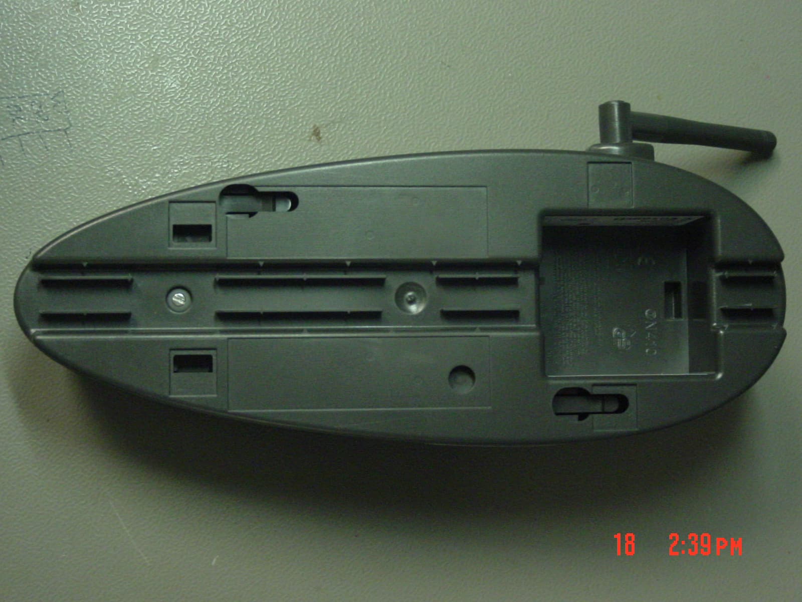
Click to zoom
Application Details
- Equipment Class
- DXX - Part 15 Low Power Communication Device Transmitter
- Date of Grant
- Sep 05, 2006
- Application Purpose
- Original Equipment
- Date of Application
- Sep 05, 2006
- Equipment Note
- CORDLESS SCANNER BASE UNIT
- Frequency Range
- 2402.00000000 - 2480.00000000
- Company
- Symbol Technologies Inc
- Country
- United States
Documents & Files
Document Text
Text extracted from the exhibit documents filed with the FCC. Open a document above to read the original.
Users Manual
PL370/470 Cradle Quick Reference Guide 2PL370/470 Cradle © 1999 - 2006 SYMBOL TECHNOLOGIES, INC. All rights reserved. Symbol reserves the right to make changes to any product to improve reliability, function, or design. Symbol does not assume any product liability arising out of, or in connection with, the application or use of any product, circuit, or application described herein. No license is granted, either expressly or by implication, estoppel, or otherwise under any patent right or patent, covering or relating to any combination, system, apparatus, machine, material, method, or process in which Symbol products might be used. An implied license exists only for equipment, circuits, and subsystems contained in Symbol products. Symbol and the Symbol logo are registered trademarks of Symbol Technologies, Inc. Other product names mentioned in this manual may be trademarks or registered trademarks of their respective companies and are hereby acknowledged. Symbol Technologies, Inc. One Symbol Plaza Holtsville, N.Y. 11742-1300 http://www.symbol.com Warranty For the complete Symbol hardware product warranty statement, go to: http://www.symbol.com/warranty. Patents This product is covered by one or more patents. For patent information go to: http://www.symbol.com/patents. Quick Reference Guide3 Introduction The PhaserLink 370/470 Radio Frequency (RF) cradle acts as a stand, host communication interface and a charger for the Phaser RF scanner. For convenience, the cradle can sit on a desktop or be mounted on a wall. The cradle receives data from the scanner via radio frequency (RF) transmissions through the antenna, then transmits that data to the host device through an attached cable. The cradle also charges the scanner’s battery pack (in the scanner). Two versions of the cradle are available: • PL470 cradle: radio retail version. • PL370 cradle: radio industrial version. This Quick Reference Guide provides basic instruction on the set up and use of the cradle. Unless otherwise noted, the term PhaserLink refers to all versions of the cradle. Equipment Supplied The following equipment is supplied: -Two Screws (for wall mounting). -One Velcro strip (for desk mounting). -Four rubber feet (for desk mounting). -This Quick Reference Guide. -PhaserLink cradle. Save the shipping container for storing or shipping. Inspect all your equipment for damage. If anything is damaged or missing, call your authorized Customer Support Representative immediately. Related Documentation -P370/470 RF Scanner Product Reference Guide, p/n 72-38495-xx -P370/470 RF Scanner Quick Reference Guide, p/n 72-38493-xx. 4PL370/470 Cradle Parts Connecting to the Host Scanner Support Tab Charging/ Communication Contacts Charging LED COM 1 Port Power Port Wall-mounting Socket 2 Antenna Wall-mounting Socket 1 Pairing Label COM1 Power Port To connect the cradle to a host: 1.Insert the appropriate interface cable from the host computer into the COM1 port. 2.Connect the power connector of the power supply (p/n 50-19000-101) into the cradle power port. (The cradle cannot be powered by the host computer.) 3.Connect the appropriate line cord to the power supply and the other end to an AC power source. Quick Reference Guide5 Wall Mounting Before wall-mounting the cradle, the scanner support tab must be changed from the desk-mount position to the wall-mount position.. Desk MountWall Mount 1.Lift the scanner support tab out of the top part of the cradle and replace it in the wall-mount position as shown. 2.Seat the cables from the bottom of the cradle in the grooves along the length of the cradle so that the bottom of the cradle is smooth and flat. 3.Secure two screws (included) to the wall. A template is provided on page 14. -Fasten the screws provided into the wall where the cradle should hang, leaving about 1/8” (0.3 cm) of the screw outside the wall for the cradle wall mounting sockets. 4.Place the cradle over the screw heads and slide down until it fits into place. Slight pressure upwards should not move the cradle. 5.Position the antenna vertically, pointing toward the ceiling. 6.Place the Phaser scanner in the cradle. 1 2 Cable Grooves 3 6PL370/470 Cradle Inserting Phaser in the Cradle Place the Phaser scanner in the cradle so that the top of the scanner sits in the larger part of the cradle and the metal contacts on the bottom of the scanner touch the contacts on the cradle. Pairing The wireless connection between the scanner and cradle is the low power radio transmission through RF transceivers in both the scanner and cradle. Communication consists of bidirectional message packets. However, the scanner and cradle must be paired for this communication to work. To pair the scanner with the cradle: 1.Scan the pairing bar code on the top of the cradle. A duplicate pairing bar code is located in the well on the bottom of the cradle. 2.Insert the scanner into the cradle (recommended but not required). Note that data cannot be scanned until linking (pairing) is complete. 3.During pairing there is an exchange of information between the scanner and the cradle. This occurs in a few seconds if the scanner is in the cradle and over a minute if the scanner is not in the cradle. 4.After the exchange is complete, the scanner and cradle are paired. Successful pairing is indicated by a warble beep; failure, or unsuccessful pairing, is indicated by a low/high beep. Sending Data to the Host Computer The cradle receives data from the scanner and transmits it to the host computer via the interface cable. Recharging the Battery in the Phaser To charge the scanner’s battery, place the scanner in the cradle ensuring the metal contacts on the bottom of the scanner touch the contacts on the cradle. A NOTEAfter a new host is installed at the cradle, re-scan the pairing bar code. This allows the cradle to notify the scanner of the change in the host device. Quick Reference Guide7 complete charge takes up to 4 hours, depending upon the remaining charge in the …
Text truncated - open the document above for the full version.
ID Label/Location Info
Symbol Technologies, Inc. • One Symbol Plaza, Holtsville, NY 11742-1300 • 1.631.738.5134 • www.symbol.com July 19, 2006 Regulatory Engineering Re: Exhibit 9 – Label & Label location FCC ID: H9PL470 Respectfully, Mark S. Luksich Director, Regulatory Engineering 631-738-5134 [email protected]
Operational Description
71-61643-01 Rev B Theory of Operation (Mesa RF Scanner) Symbol Confidential Unless marked otherwise, printed copies are uncontrolled Page 1 of 20 REV DESCRIPTION DATE Author A Initial Release Per EDR712 11/20/2003 J. Chin. B Updated part numbers for RoHS EC24058 05/04/2006 C.Klicpera Theory of Operation: Mesa Scanner DOC. NO: 71-61643-01 Rev.B Theory of Op: Mesa Scanner Page 1 of 20 71-61643-01 Rev B Theory of Operation (Mesa RF Scanner) Symbol Confidential Unless marked otherwise, printed copies are uncontrolled Page 2 of 20 Theory of Operation: Mesa Scanner 1. Purpose The purpose of this document and the respective schematic is to provide a complete description of the detailed design of the Mesa RF (a flat top derivative of the Phaser RF) scanner hardware subsystem. 2. References [1] Schematic: Mesa Scanner PCB 17-83514-01, RoHS; 17-61643-01, non-RoHS [2] Vanguard RF System Definition Document 00-09845-SD0 [3] Vanguard RF Software Functional Specification 00-09845-FS0 [4] Vanguard Microprocessor Selection Update, June 25, 1997, Tom Bianculli (Project Folder) [5] Microprocessor Update for Vanguard Project, September 19, 1997, Tom Bianculli (Project Folder) [6] Theory of Operation: Vanguard RF Base 71-36036-01 [7] Printed Circuit Board Design Techniques for EMC Compliance, Mark I. Montrose [8] Thorough tolerance analysis of a resistor divider auto-ID scheme, Kevin Cordes (Project Folder) [9] Schematic: Vanguard RF Handle PCB 17-82498-01, RoHS; 17-36035-01, non-RoHS [10] Vanguard Radio Theory of Operation (Project Folder) [11] Patent: An RF encoding scheme for UART communications Docket # [12] Patent: UART Synchronization for RF communication Docket # 748 [13] Analysis of the performance impact by processing raw radio data, Dana DeMeo (Project Folder) 3. Overview The P370 flat top (“Mesa”) scanner is a direct line extension to the P370 Phaser scanner. It is derived from the P370 by removing the keypad and display creating what is essentially a LS3070 replacement. Many parts are shared with the existing P370 line; however, a new main PCB and flex board are required to compensate for the missing display and keypad. The “flat top” of the unit is inherited from the P304 corded scanner. Section 4 details the differences between the keypad and display Phaser RF scanners and Mesa. The system is powered by a single 3.6V Lithium Ion cell, stepped up to 5V by a SEPIC DC-DC converter. The scanner contains a small PCB in the handle to hold the trigger, battery contacts and connection to external contacts. A second PCB in the head of the scanner (the main PCB) contains the DC-DC converter, the radio and the entire digital system. LEDs and beepers, the only user interface on the scanner, are located on the top as in the P304. An SE1200-family scan engine is used to provide scanning capability and is connected to the main PCB via a flex cable. The handle board is also connected to the main PCB with a flex cable. 71-61643-01 Rev B Theory of Operation (Mesa RF Scanner) Symbol Confidential Unless marked otherwise, printed copies are uncontrolled Page 3 of 20 The digital system has been designed to decode 100 scan/second one dimensional data; support for 2-D symbologies is not included. References [4] and [5] detail the requirements needed to obtain the requisite 1-D performance and provides benchmark data which justifies the core architecture chosen for this design. The radio system is designed to communicate 100 feet reliably. Calculations show that using 8dBm transmit power, with –85dBm sensitivity, the radios should meet this requirement with sufficient margin. In order to achieve the highest antenna gain possible and still remain inside the scanner, an inverted-F type antenna is used. It sits high up in the front, directly above the scan engine. The center conductor and two ground pins connect to the PC board using compliant pins. The base uses a center-fed split dipole external rubber-duck antenna, with excellent gain and radiation patterns. The radios use metal covers that snap onto a metal “fence” that is soldered to the PCB. This technology allows easy shield removal to gain access to the radio components. 4. Comparing Mesa to Phaser RF Visually, the Mesa and its Phaser RF siblings are fairly similar. The major external difference is Mesa’s lack of an LCD display and keypad. The P304’s top bezel is used, with identical LED and beeper locations. Note that the metal hook bar has no embossed logo, unlike the P304. The P370 cradle and power supply are used without any changes. Internally, a new main PCB and flex board have been created. The PCB is very similar to the Phaser RF main PCB. However, leads to/from the microprocessor for the LCD and keypad have been removed. This leaves microprocessor pins 56-59 and 94 unused and floating. Subsets of the address and data buses are no longer used to drive and collect signal from the keypad, as it does not exist in Mesa. The LEDs and beeper in Mesa are different than those in Phaser RF, so the driver circuits for these elements are updated. Support for short-range and advanced long-range scan engines is retained. The ENTER key is used to wake the Phaser RF scanner from sleep and forcibly reset the unit. That functionality does not exist in Mesa, so the ENTER/ON* inputs to the wakeup and reset circuitry are eliminated. Pull-up resistors tied to Vcc are either left in place as is or added to compensate for this deletion. Microprocessor pin 9 is left floating. The new flex board design features the LED and beeper locations from P304, as well as current-limiting resistors for the LEDs. The 18-pin connector and its complementary socket on the PCB are held over from Phaser, although the cable pinout is wholly different. Mesa’s flex board pinout was arranged such that accidentally connecting a Mesa flex to a Phaser RF main PCB would not cause a dangerous situation (Vcc-ground short, etc). The opposite situation is also safe; connecting a Phaser RF flex to a Mesa main…
Text truncated - open the document above for the full version.
Parts List/Tune Up Info
Number Qty Description RoHS Compliant Ref Des Item Type 50-11558-4R7 1 CAP:CG,0603, 5%, 50V,4.7PF Yes C303 Component 50-11558-220 9 CAP:CG,0603, 5%, 50V,22PF Yes C304,C306,C307,C311,C314,C316,C317,C320,C3 25 Component 50-11558-181 1 CAP:CG,0603, 5%, 50V,180PF Yes C305 Component 50-11558-330 2 CAP:CG,0603, 5%, 50V,33PF Yes C308,C319 Component 50-11561-103 5 CAP:XR,0603,10%, 50V,0.01UF Yes C309,C348,C351,C363,C388 Component 50-11532-103 12 CAP:X7R,0402,10%,16V,10000PF Yes C310,C318,C323,C339,C341,C344,C346,C357- C359,C371,C390 Component 50-11558-1R2 2 CAP:CG,0603, B%, 50V,1.2PF Yes C312,C321 Component 50-21500-075 4 CAP:Y5V,0805,Z%,16V,1.0UF Yes C324,C349,C356,C360 Component 50-11558-3R3 1 CAP:CG,0603, 5%, 50V,3.3PF Yes C326 Component 50-11560-102 2 CAP:XR,0603, 5%, 50V,1000PF Yes C334,C389 Component 50-11563-560 1 CAP:CG,0402, 5%, 25V,56PF Yes C337 Component 50-11560-122 2 CAP:XR,0603, 5%,50V,1200PF Yes C342,C345 Component 50-11563-220 2 CAP:CG,0402, 5%, 25V,22PF Yes C343,C367 Component 50-11562-121 1 CAP:CG,0603, 1%,50V,120PF Yes C350 Component 50-11570-475A010 1 CAP:TA,A,20%,10V,4.7UF Yes C361 Component 50-11558-391 1 CAP:CG,0603, 5%, 50V,390PF Yes C362 Component 50-11569-474A035 1 CAP:TA, A,10%, 35V,0.47UF Yes C365 Component 50-11569-225A6R3 1 CAP:TA, A,10%,6.3V,2.2UF Yes C366 Component 50-11565-104 21 CAP:XR,0603,10%, 16V,0.1UF Yes C38,C52,C53,C55,C70,C73- C76,C79,C85,C86,C92,C93,C95-C98,C100,C103,C302 Component 50-11500-312 2 CAP:XR,0805,10%, 16V,.22UF Yes C45,C54 Component 50-11571-226D025 3 CAP:TA,D,20%,25V,22UF,.200ESR Yes C50,C87,C91 Component 50-21500-076 1 CAP:Y5V,1206,16V,4.7UF,+80-20% Yes C59 Component 50-11558-101 3 CAP:CG,0603, 5%, 50V,100PF Yes C60,C313,C364 Component 50-11562-270 2 CAP:CG,0603, 1%, 50V,27PF Yes C67,C72 Component 50-11561-102 9 CAP:XR,0603,10%, 50V,1000PF Yes C77,C78,C80-C84,C101,C102 Component 50-11500-299 1 CAP:XR,1206,10%,16V,1.0UF Yes C94 Component 50-11570-106B016 1 CAP:TA, B,20%, 16V,10UF Yes C99 Component 50-13705-012 1 DIODE:TVS,300W,12V,SOT-23 Yes CR1 Component 50-13707-001 1 LED:RED,6.2 MCD,660NM,R/A,SM * Yes with Exemptions CR2 Component 50-14800-369 1 DIODE:SCTKY,MBRS340T3, SMD Yes CR3 Component 50-14803-2R7 1 DIODE:ZENR,BZX84C,5%,2.7V,SOT23 Yes CR308 Component 50-04800-177 3 DIODE:1N4148/914,SWIT,SOT-23 Yes CR4,CR6,CR7 Component 50-14800-402 1 DIODE:BAR74,SWTG,50V,SMT Yes CR5 Component 50-14803-6R8 1 DIODE:ZENR,BZX84C,5%,6.8V,SOT23 Yes CR8 Component 50-22700-046 1 FILTER:RF,BP,LC,2.45GHZ,EXT,SM Yes FL301 Component 50-12700-105 1 FILTER:RF,BP,10.7MHZ, SM Yes with Exemptions FL302 Component 50-12100-1554 1 CONN:PWR,DC,M,JCK,2,R/A,1.65MM Yes J3 Component 50-12100-1589 1 CONN:COAX,RCPT,CBL,TERM SM * Yes J301 Component 50-12100-1501 1 CONN:MOD,JACK,RJ,10,PCB,R/A, * Yes J5 Component 50-11800-306 2 FERRITE BEAD:.22X.20,600OHM,3A Yes L14,L17 Component 50-11800-319 1 FERRITE CHIP:1206,80 OHM,3.0A* Yes L2 Component 50-11800-294 13 FERRITE CHIP:0805,600 OHM, * Yes L3,L5,L10-L13,L15,L16,L18-L22 Component 50-11826-220 4 IND:0603,10%,0.3A,22NH Yes L304,L307,L324,L325 Component BoM Report PL 4 70 Page 1 of 4 Number Qty Description RoHS Compliant Ref Des Item Type BoM Report PL 4 70 50-11826-3R3 3 IND:0603,10%,0.3A, 3.3NH Yes L306,L309,L322 Component 50-11826-2R7 1 IND:0603,10%,0.3A,2.7NH Yes L308 Component 50-11800-323 1 FERRITE CHIP:0603,EMI,200MA * Yes L310 Component 50-11800-449 1 IND:CH,5%,155MA,1.5UH,1206 Yes L311 Component 50-11826-1R8 1 IND:0603,10%,0.3A,1.8NH Yes L323 Component 50-21816-1R2 1 IND:0805,10%,50MA,1.2UH Yes L326 Component 50-24800-109 1 TRSTR:MMBT3904,SN,AMP,SOT-323 Yes Q300 Component 50-24800-119 2 TRSTR:6306,P-CH,DUAL,20V,SOT-6 Yes with Exemptions Q302,Q303 Component 50-04800-195 2 TRSTR:2N7002,NCH,MOSFET,SOT-23 Yes Q4,Q8 Component 50-14800-412 1 TRSTR:9934,P-CH,DUAL,SO-8 Yes Q5 Component 50-04800-191 1 TRSTR:DTC114EK,SN,DIG,SOT-23 Yes Q6 Component 50-04800-174 1 TRSTR:2N3904,SN,GEN,SOT-23 Yes Q7 Component 50-14791-472 7 RES:CH, 0603, 5%,.063W,4.7K Yes R2,R69,R72,R73,R77,R334,R336 Component 50-14785-472 1 RES:CH, 0402, 5%,.063W,4.7K Yes R302 Component 50-14791-100 3 RES:CH, 0603, 5%,.063W,10 Yes R303,R345,R425 Component 50-14785-100 2 RES:CH, 0402, 5%,.063W,10, LF Yes R306,R307 Component 50-14791-181 1 RES:CH, 0603, 5%,.063W,180 Yes R308 Component 50-14791-470 1 RES:CH, 0603, 5%,.063W,47 Yes R309 Component 50-14785-510 1 RES:CH, 0402, 5%,.063W,51 Yes R310 Component 50-14791-620 1 RES:CH, 0603, 5%,.063W,62 Yes R311 Component 50-14791-562 1 RES:CH, 0603, 5%,.063W,5.6K Yes R318 Component 50-14785-102 1 RES:CH,0402,5%,.063W,1.0K,LF Yes R320 Component 50-14791-333 1 RES:CH, 0603, 5%,.063W,33K Yes R321 Component 50-14750-032 2 RES,V:1TRN,3MM,0.15W,500,SM * Yes R322,R335 Component 50-14785-513 2 RES:CH, 0402, 5%,1/16W,51K Yes R324,R331 Component 50-14785-152 1 RES:CH, 0402, 5%,.063W,1.5K,LF Yes R326 Component 50-14791-473 1 RES:CH, 0603, 5%,.063W,47K Yes R329 Component 50-14791-510 1 RES:CH, 0603, 5%,.063W,51 Yes R330 Component 50-14791-471 1 RES:CH, 0603, 5%,.063W,470 Yes R333 Component 50-14791-683 1 RES:CH, 0603, 5%,.063W,68K Yes R337 Component 50-14791-332 3 RES:CH, 0603, 5%,.063W,3.3K Yes R347-R349 Component 50-14785-222 1 RES:CH, 0402, 5%,.063W,2.2K,LF Yes R350 Component 50-14785-181 1 RES:CH, 0402, 5%,.063W,180,LF Yes R351 Component 50-14785-471 1 RES:CH, 0402, 5%,.063W,470 Yes with Exemptions R352 Component 50-14700-219 1 RES:CH,0603,0.1%,.063W,1.91K Yes with Exemptions R4 Component 50-14714-40R2 1 RES:CH, 0603, 1%,.063W,40.2 Yes with Exemptions R40 Component 50-14714-2740 1 RES:CH, 0603, 1%,.063W,274 Yes R45 Component 50-14700-221 2 RES:CH, 1206, 1%,.250W,.1 OHM Yes R47,R56 Component 50-14714-1002 8 RES:CH, 0603, 1%,.063W,10.0K Yes R48,R59,R60,R62,R83,R319,R327,R328 Component 50-14714-1001 9 RES:CH, 0603, 1%,.063W,1.00K Yes R49,R66,R305,R315,R325,R342-R344,R428 Component 50-14700-190 2 RES:CH,0603,0.1%,.062W,2K OHMS Yes R52,R57 Component 50-14700-191 2 RES:CH,0603,0.1%,.062W,38.3K OHMS Yes R53,R55 Component 50-14700-218 1 RES:CH,0603…
Text truncated - open the document above for the full version.
Schematics
VIN TAB GND VC FB VSW S/S IFB VCC VCC ++ VOVI COM VCC HC14 + + HC126 HC126 VCC HC125 TLC2272 TLC2272 OFSHEET TEST ENG. DIMENSIONS ARE IN CHECKED MFG. ENG. PRODUCT QUALITY DRAWN ENGINEER REV QTY. DESCRIPTIONREMARKS/REF.SYMBOL PART NO. Bohemia, New York SYMBOL TECHNOLOGIES INC. DWG. NO. REV APPROVALSDATE PARTS LIST .XX .XXX MMINCH ANGLES MATERIAL: FINISH: FRACTIONS SIZE NEXT ASSYUSED ON ITEM + - + - + - + - DO NOT SCALE DRAWING THE DWG. AND SPECIFICATION CONTAINED HEREON ARE PRO- PRIETARY AND MUST NOT BE USED, COPIED, REPRODUCED OR OTHERWISE DEALT WITH NOR ITS CONTENTS COMMUN- ICATED TO OTHERS EXCEPT IN ACCORDANCE WITH WRITTEN SYMBOL TECHNOLOGIES INC. INSTRUCTIONS RECEIVED FROM UNLESS OTHERWISE SPECIFIED 1 2 4 5 6 78 A B C D 8654 3 2 1 A B C D 3 77 + - + - ZONE DESCRIPTION E.C.BYAPVD.DATE No. REVISIONS SPARES CHANGES FROM REV A TO REV B: NOTES: CHANGE R54 AND R4 FROM 511/221 OHMS TO 4.32K/1.91K OHMS. 1) ALL CAPACITORSARE 50V, 10% UNLESS OTHERWISE INDICATED 2) ALL RESISTORS ARE 1/16 WATT, 5% UNLESS OTHERWISE INDICATED 3) THE SRAM U5 WILL BE 32KX8 UPGRADABLE TO 64KX8 OR 128KX8 6/5/06MB MB 6/20/06 M. BLASCZAK C. KLICPERA 6/20/06 6/20/06 6/20/06 Tue Jun 20 10:09:04 2006 8 4 1 3 2 U18 84 7 56 U18 C A CR8 11 13 12 U19 11 13 12 U20 8 10 9 U20 C103 C102 99 98 103 102 101 100 C101 C99 89 U15 13 CR5 CR4 C86 R58 16 C85 C77 18151412 10 C70 6 OI C VR5 C60 R49 3 4 6 5 Q5 L2 2 8 R56 R53 R52 L3 C54 1 21 20 19 17 R55 R57 C79 C59 R54 C53C52 C84C83 C75 C82 C80 C78 C76 C74 C73C55 C81 3 11 9 7 5 4 R48 S G D Q8 CR3 R47 C87C91 4 32 1 T1 C38 C45 R45 R40 5 7 1 TAB 6 3 4 2 U17 R4 C50 PHASER RF BASE PC BOARD 17-83835-01 A A 0.1 1% 1/8W ROHS LT1513 0.1UF 16V 0.22UF BEAD 16V CHG_CURRENT .1% 3 INCHES .01 6 0.1UF 78M05 ROHS 0.1% 1.91K ROHS 4.32K 0.1% ROHS 40.2 1% CHARGE_ENB* 10UF 2K .005 1 1/64 O 1 38.3K 0.1UF 16V 5% 1K .1% V_SUPPLY V_SUPPLY BATT_SENSE+ 1% 10K 16V 0.1UF 1000PF 22UF 1000PF 16V BAR74 16V NOT_USED 16V 0.1UF 100PF 1% SI9934DY 25V 1B 16V 0.1UF 1000PF1000PF 16V 0.1UF 1000PF 1000PF 1000PF 16V 16V 0.1UF 16V 0.1UF 16V 0.1UF 1000PF 16V 16V 1% MBRS340T3 V_CHARGE 2K .1% .1% CTX10-4 * 38.3K 1000PF 4.7UF 0.1UF 0.1UF BATT_SENSE+ 16V +80/-20% 0.22UF 2N7002 SO14 ROHS V_SUPPLY 1N4148 16V BEAD 25V 274 0.1UF V_SUPPLY BZX84C6V8 25V 22UF 22UF 1/8W 0.1 1% RELEASE PER PPD #87181 RELEASE PER EDR #78529 OFSHEET REV Bohemia, New York SYMBOL TECHNOLOGIES INC. DWG. NO. REV SIZE 1 2 4 5 6 78 A B C D 8654 3 2 1 A B C D 3 77 ZONE DESCRIPTION E.C.BYAPVD.DATE No. REVISIONS HC14 VCC VCC VCC VCC HC14 V- C2- C2+ R2IN T2OUT R1IN T1OUT V+ C1- C1+ R2OUT T2IN R1OUT T1IN VCC 10K 10K VCC VCC HC14 - - - - - - - - - - - - - - VCC - - PB2/TO4 PB3/TO5 PB4/TI6/INT6 PB5/TI7/INT7 PB6/TO6 PB7/INT0 P10/D8 P11/D9 P12/D10 P13/D11 P14/D12 P15/D13 P70/PG00 P16/D14 P17/D15 P77/PG13 P76/PG12 P75/PG11 P74/PG10 P73/PG03 P72/PG02 P71/PG01 P80/TXD0 P81/RXD0 P85/SCLK1 PA2/TO1 PA3/TO3 P84/RXD1 P83/TXD1 P82/CTS0*/SCLK0 P93/AN3 P92/AN2 P91/AN1 P90/AN0 CLK WDTOUT* WR* RD* P62/CS2* P61/CS1* P60/CS0* P52/HWR* P53/BUSRQ* P54/BUSAK* P55/R/W* P64/RAS* P63/CS3*/CAS* P65/REFOUT* D3 D2 D1 D0 D4 D7 D6 D5 PA0/WAIT* PA1/T1O NMI* RST* AM8/16* EA* AGND VREF A16/P20 A17/P21 A18/P22 A19/P23 A20/P24 A21/P25 A22/P26 A23/P27 A11 A12 A13 A14 A15 A6 A7 A8 A9 A10 A1 A2 A3 A4 A5 A0 X2 X1 PB0/TI4/INT4 PB1/TI5/INT5 VCC VCC VCC DATA GND VCC DQ4 DQ3 A18 A17 A16 A15 A14 A13 A12 A11 A10 A9 A8 A7 A6 A5 A4 A3 A2 A1 DQ7 DQ6 DQ5 DQ1 DQ0 DQ2 A0 CE*OE*WE* HC125 HC125 HC125 HC126 HC126 VCC VCC 26 23 21 24 25 10 19 18 17 16 15 13 12 11 222027 9 8 7 6 5 4 3 2 NC 1 A9 A8 A7 A6 A5 A4 A3 A2 A1 A0 D6 D7 D5 D1 D2 D3 D4 RAM OECE 256KRAM 32KX8 14 A 13 A A 12 11 9 8 10 A A A A A 7 2 3 4 5 6 A A A A A 1 A A 0 WE IO 5 4 3 6 7 IO IO IO IO IO 2 0 IO 1 IO D0 A16 A15 A14 A13 A12 A11 A10 OECE2CE1WE HC14 HC14 A NOTE: IM_AM_NOT_A_SCANNER 50K-150K INTERNAL PULLUP CONTACTS RADIO INTERFACE DO NOT POPULATE U14TO HOST A PC BOARD 17-83835-01 3 10K PHASER RF BASE SERSTAT CS_FLASH2* 10 SEE SHEET 1 12 A<18..0> CHARGE_ENB* ROHS ROHS 16V 0.1UF RTSOUT* RF_SYNTH_CLK ROHS ROHS 8128_256KRAM SM12 BEAD ROHS BEAD ROHS 8.2K 1N4148 1N4148 SMAJ12C BEAD BEAD BEAD SYN_CLK * V_SUPPLY V_SUPPLY A<0> 24.800MHZ 100K 0 16 15 20K 17 18 17 18 4.7K DS2401TSO NOT_USED 100K 100K 33 33 TMP95C061A0.1UF 16V 0.1UF 16V BEAD 0.1UF 16V 27PF27PF SFLX100 220 2N3904 7 10K 10K 1K 6 5 4 3 2 1 2N7002 0 16V 0.1UF 0 1 2 3 4 SMAJ12C 5 6 DTC114EK 7 220 4.7K 0 16V 1 2 4.7K 4.7K 220 3 BEAD BEAD BEAD 33 33 4 1/16W 200 4.1V0.1UF 16V 5 6 0 7 16 15 14 13 11 10 9 8 7 6 5 4 3 2 1 00 16 15 14 13 12 11 10 9 8 7 6 5 4 3 2 1 13 12 11 9 8 7 6 5 4 3 2 1 0 14 100K SMAJ12C 2 SSN_DATA SSN_DATA TXD1 DTR CTSIN RTSOUT RXDIN* TXD0 RXD0 RXD1 RF_CARR_SENSE COMMAND_MODE* BATT_SENSE+ RESET* CS_SRAM* RF_RXV_ENB* TRISTATE_ENB* SYN_DATA CS_SRAM* CS_FLASH2* WR* CTSIN* SYN_CLK LED* RF_VCC_ENB* SCANNER_ON* RF_CS COMMAND_MODE* RF_RXV_ENB* CTSIN* RESET* BATT_SENSE+ CHG_CURRENT RF_SYNTH_DATA RD* RF_SYNTH_LATCH RF_TXD RF_SYNTH_REF RF_SYNTH_CLK RF_SYNTH_DATA RF_TXV_ENB* RF_RXD RF_CS RF_VCC_ENB* SCANNER_ON* RTSOUT* SYN_DATA LED* V_CHARGE RF_/RXV_ENB* WDT_OUT* SERCTL* SERCTL SCAN/RF_COMM* RXD0 TXD0 SCAN/RF_COMM* RF_TXD SCAN/RF_COMM* SCANNER_PRESENT* RD* WR* SWITCHED_POWER RF_RXD 4.7K BEAD 220 0.1UF 10K 16V 1UF D<7..0> LM4040 NOT_USED 28SF040_32MULTI_ALGOR SCAN/RF_COMM* WR* RD* A<1> A<2> A<6> A<8> A<9> A<10> A<13> A<14> A<15> A<16> A<11> A<12> A<4> A<3> A<7> A<5> * SI9934DY M04-730A0 BEAD ROHS ROHS TXDOUT* BEAD SCANNER_PRESENT* RF_TXV_ENB* SCAN/RF_COMM* CTSIN* RMODBDL * CCDLF-8000 ROHS BEAD BEAD * CCDLF-8000 ROHS * CCDLF-8000 ROHS * CCDLF-8000 ROHS * CCDLF-8000 ROHS * CCDLF-8000 ROHS * CCDLF-8000 ROHS CCDLF-8000 * ROHS LT1381 ROHS 1/10W 150 1101F-RED ROHS RF_SYNTH_REF RF_SYNTH_LATCH U13 87 86 85 84 83 82 81 80 79 78 77 76 75 74 73 72 71 70 69 68 67 66 65 64 17 24 25 45 46 47 48 49 50 51 52 29 10 53 54 55 56 57 58 59 60 90 91 92 93 94 96 97 98 99 1 2 3 4 5 6 7 8 9 11 12 13 14 15 16 20 21 22 23 32 33 34 35 36 37 38 39 40 41 42 43 88 30 18 31 89 27 28 C67C72 817263 RN1 54 63 RN2 7 2 5481 29 35 41 23 26 30 36 42 4…
Text truncated - open the document above for the full version.
Test Report
Retlif Testing Laboratories R Test Report No. R-11560-1 Page 3 of 55 Table of Contents List of Figures.....................................................................................................................4 List of Tables.......................................................................................................................5 Certification and Signatures..............................................................................................6 Revision History.................................................................................................................7 Test Program Summary.....................................................................................................8 1.0 Scope................................................................................................................ 10 2.0 Applicable Documents.................................................................................... 10 3.0 Acronyms and Definitions.............................................................................. 11 4.0 General Requirements.................................................................................... 12 4.1 Test Environment ..............................................................................................12 4.1.2 Conducted Emissions................................................................................12 4.1.3 Radiated Emissions...................................................................................12 4.1.3.1 Preliminary .............................................................................................12 4.1.3.2 Formal....................................................................................................12 4.2 Test Instrumentation .........................................................................................12 4.3 Grounding of Measuring Instrument..................................................................13 4.4 Measurement Accuracy ....................................................................................13 4.5 Detector Function..............................................................................................13 4.6 Measurement Frequencies ...............................................................................13 5.0 Test Sample Description................................................................................. 14 5.1 General.............................................................................................................14 5.2 EUT Parameters ...............................................................................................14 5.2.1 Designations ..............................................................................................14 5.2.2 Physical Characteristics.............................................................................14 5.3 Configuration.....................................................................................................14 5.3.1 Leads Tested .............................................................................................15 5.4 Modifications .....................................................................................................15 5.5 Mode of Operation ............................................................................................15 5.5.1 Support Equipment ....................................................................................15 5.6 Report of Measurements ..................................................................................16 6.0 Test Methods Performed................................................................................ 18 Conducted Emissions.......................................................................................19 FCC Part 15, Subpart C, Paragraph 15.207(a).............................................19 Radiated Emissions, Fundamental & Harmonics ..............................................29 FCC Part 15, Subpart C, Paragraph 15.249(a).............................................29 Occupied Bandwidth .........................................................................................39 FCC Part 15, Subpart C, Paragraph15.249(c)...............................................39 Spurious Emissions..........................................................................................45 FCC Part 15, Subpart C, Paragraph 15.249 (c)/15.209.................................45 Duty Cycle Determination .................................................................................52 FCC Part 15, Subpart C, Paragraph 15.249(c)/15.209..................................52 Retlif Testing Laboratories R Test Report No. R-11560-1 Page 4 of 55 List of Figures Figure 1 - Test Sample Diagram .........................................................................................17 Retlif Testing Laboratories R Test Report No. R-11560-1 Page 5 of 55 List of Tables Table 1 - Test Methods and Results .....................................................................................9 Table 2 - EUT Designations................................................................................................14 Table 3 - Physical Characteristics.......................................................................................14 Table 4 - EUT Cable Configuration .....................................................................................14 Table 5 - Support Equipment ..............................................................................................15 Table 6 - Test Sequence and Results......................................................................…
Text truncated - open the document above for the full version.
Contact Information
Applicant
Qianlin Zhou(Regulatory Specialist)
Test Firm
Retlif Testing LaboratoriesMichael Bozza
Technical Specifications
| # | Rule Parts | Frequency Range | Power Output |
|---|---|---|---|
| 1 | 15C | 2.40 GHz - 2.48 GHz | - |
Other Applications from Symbol Technologies Inc

H9PCCHUB1
Jun 30, 2015Customer Concierge
Equipment Class
NII - Unlicensed National Information Infrastructure TX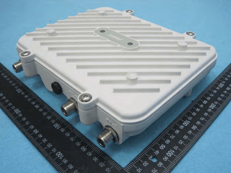
H9PAP7562
May 10, 2015802.11 abgn/ac Access Point
Equipment Class
DTS - Digital Transmission System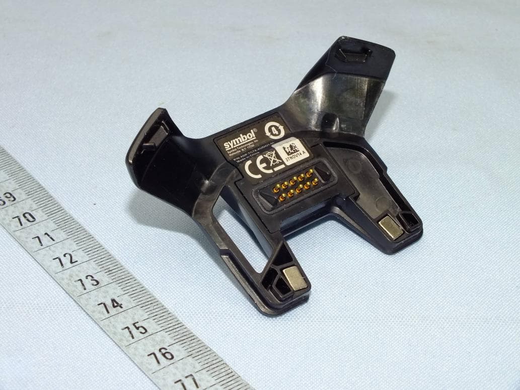
H9PTC75AH
Mar 26, 2015Touch Computer
Equipment Class
NII - Unlicensed National Information Infrastructure TX
H9PRA1202
Sep 24, 2014UHF Narrowband Radio Module
Equipment Class
TNB - Licensed Non-Broadcast Station Transmitter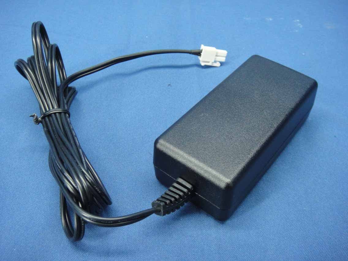
H9PEMG101
Aug 26, 2014802.15.4 Gateway
Equipment Class
DTS - Digital Transmission System